Blu LIFE 8 User manual

BLU LIFE 8
SERVICE MANUAL

CONTENT
DOCUMENTS INFORMATION................................................ERROR! BOOKMARK NOT DEFINED.
1. PHRASE AND REFERENCE LITERATURE................ERROR! BOOKMARK NOT DEFINED.
1.1 Breviary........................................................................................... Error! Bookmark not defined.
1.2 Phrase.............................................................................................. Error! Bookmark not defined.
1.3 Reference literature ......................................................................... Error! Bookmark not defined.
2. INTRODUCTION................................................................................................................................4
2.1 Compile Objective ............................................................................................................................4
2.2 Project Background...........................................................................................................................4
3. LIFE 8 SUMMARIZE.........................................................................................................................5
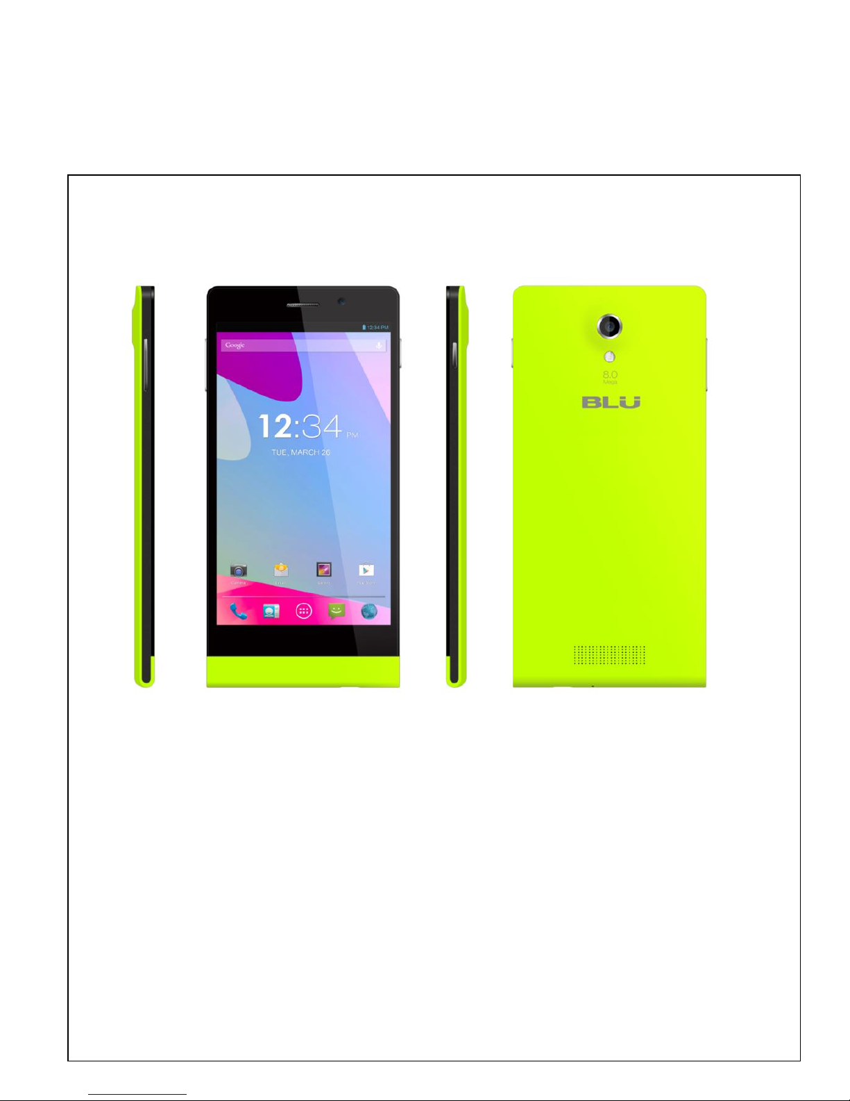
3.1 LIFE 8 product description ...............................................................................................................7
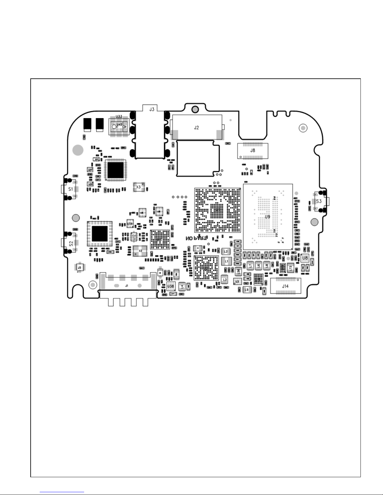
3.2 Assembly components on TOP layer as follow.................................................................................8
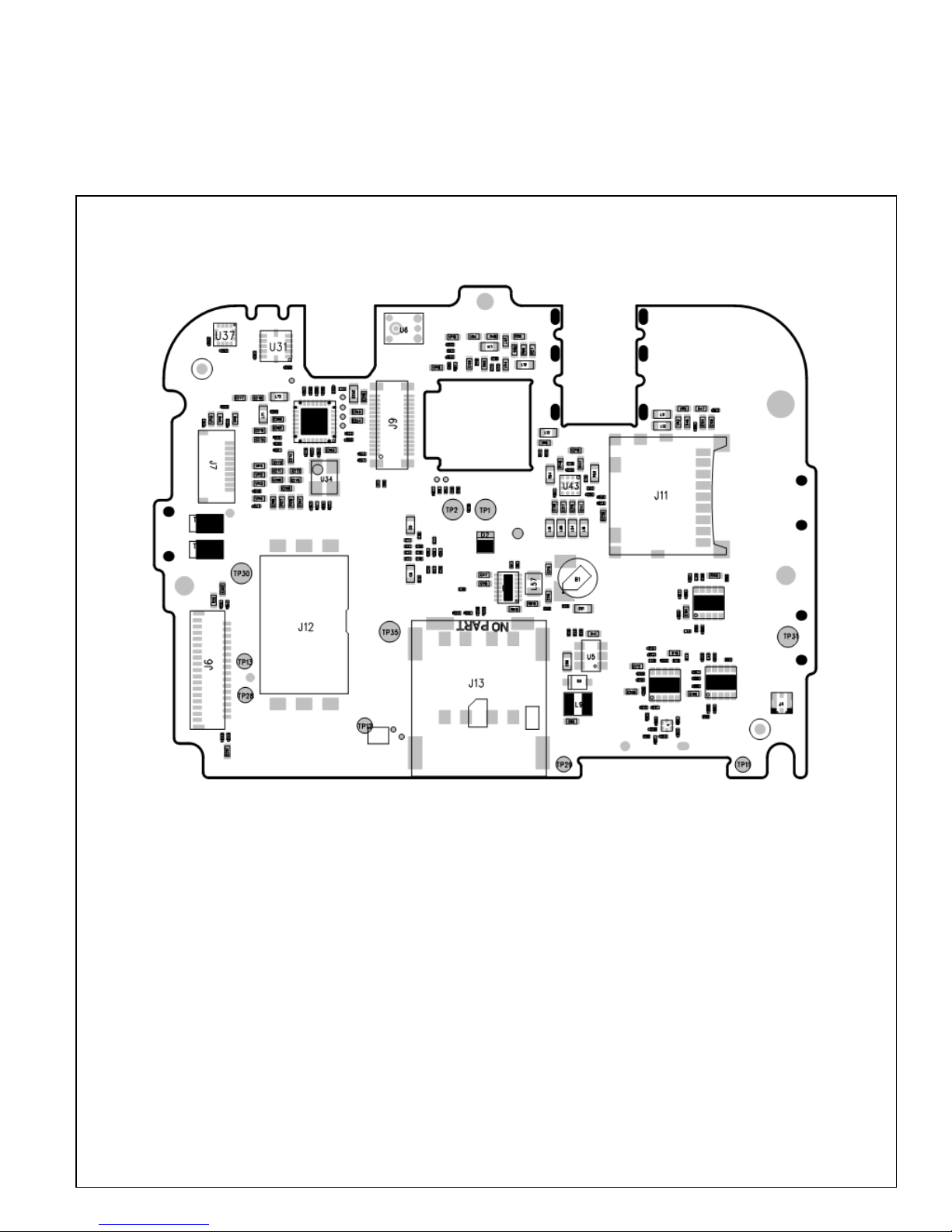
3.3 Assembly components on Bottom layer as follow:........................................................................9
3.4 LIFE 8 Hardware Diagram..............................................................................................................10
4. RF PARTS..........................................................................................................................................12
4.1 Basic diagram:.................................................................................................................................12
4.2 TX Part troubleshooting.................................................................................................................13
4.2.1 TX process analysis..............................................................................................................13
4.2.2 TX circuit troubleshooting.....................................................................................................14
4.2.3 TX circuit examine and repair flow chart ..............................................................................15
4.3 RX Circuit troubleshooting .............................................................................................................16
4.3.1 RX circuit analysis.................................................................................................................16
4.3.2 RF Part examine and Repair..................................................................................................17
4.3.3 RX examine and repair flow chart........................................................................................19
5. BASEBAND PARTS..........................................................................................................................20
5.1 Power Management Part Diagram ..................................................................................................20
5.2 Power on .........................................................................................................................................21
5.2.1 Normal Power On..................................................................................................................21
5.2.2 Schedule Power On/OFF .......................................................................................................21
5.2.3 Charge Power On...................................................................................................................22
5.2.4 Phone can not power on troubleshooting:...........................................................................22
5.3 Audio Part troubleshooting .............................................................................................................22
5.3.1 Speaker Circuit ......................................................................................................................22
5.3.2 MIC Circuit............................................................................................................................22
5.3.3 Earphone Circuit....................................................................................................................23
5.3.4 Receiver Circuit.....................................................................................................................23
5.4 Vibration issue: ...............................................................................................................................24
5.5 Download process...........................................................................................................................25
5.5.1 NAND Flash Download ........................................................................................................25
5.6 LCD Part .........................................................................................................................................25
5.7 CTP Part..........................................................................................................................................26
5.8 Camera part.....................................................................................................................................26
5.9 SIM card issue:................................................................................................................................26

5.10 Charge function:.........................................................................................................................27
6. DEFECT DESCRIPTION ABBREVIATION.................................................................................28
7. THE TAG ...........................................................................................................................................29

1. INTRODUCTION
1.1 Compile Objective
This document, is the maintenance work guide for LIFE 8. The compile objective is to
describe the detail theory of LIFE 8 and to offer a maintenance guide for the later mass
production and after service.
The readers of the document should be the debug worker of SMT and after-service. It will
be the work guide for them. At the same time, the other members of the LIFE 8 project
group can also refer to the document.
1.2 Project Background
LIFE 8 is a new product candybar smart phone with touch keys, and six band 3G project
designed by us, it based on the platforms from MTK, according to the marketing evaluation.
Project name:LIFE 8

2. LIFE 8 Summarize
LIFE 8 is a project developed on MTK(MT6592, 8 cores) Platform. The mainboard system
is composed of RF part(MT6166),WIFI/BT/GPS part(MT6625) ,PMU
parts(MT6322+MT6333) and BB part (MT6592).
LIFE 8 supports six frequency bands, include GSM qual bands and WCDMA two bands.
Support GSM850MHz, GSM900MHz, DCS1800MHz , PCS1900MHz, WCDMA
900MHz and WCDMA2100MHz. It is supports Dual-cards-two-standby. LIFE 8 size is
118*63*12mm, with three touch keys. It have 8Mega rear camera internal and 1.6Mega
front camera, LCD is 5 inch with 16Mega colors and HD(1080*720) pixels display. It
supports dual bands WIFI(2.4G and 5G band). which support micro SD card extension up
to 32GB.

Product detail parameters as follow:
Form
Candybar,
OS
Android 4.2.2
BAND
GSM 850/900/1800/1900 MHz
WCDMA:900/2100MHz
Net
Hsdap+ hsupa
Flash Memory (Bits)
eMMC flash 8GB
RAM (Bits)
DDR2 8Gb
Battery
Li-ion 2000 mAh
Talking time
<=15 Hous
Standby time
Dual SIM card<=200 Hous
Single SIM card<=240 Hous
MP3 playback time
<=7Hous, maximum volume
and speaker on
Size
118*63*12mm
Target weight
110g
Mai LCD
5inch IPS 16Mega
colors HD(1080*720)
Antenna
Internal PIFA
Memory extension
Micro SD Card( 32 GB )
Bluetooth
4.0
WIFI
Yes,2.4G,5G 802.11a/b/g/n
Camera
Internal, 8Mega rear and
1.6Mega front
Audio
Yes, i-Melody, MP3, WAV,
MIDI, AMR
Vedio
Yes, H.265…
Headset
Yes, stereo, 3.5mm
Flash light or torch
Yes

2.1 LIFE 8 product description
Product review

2.2 Assembly components on TOP layer as follow

2.3 Assembly components on Bottom layer as follow:

2.4 LIFE 8 Hardware Diagram
The HW Diagram as follow:

LIFE 8 Main Components of Mainboard parts
U1
CPU MT6592
U9
Memory H9TP17ABLDMCNR-KGM
X2
RF 26M Crystal
U10
power amplifier and ASM
SKY77590
U37
G-sensor BMC150
U22
RF Transceiver MT6166
X201
32.768K crystal
J4
RF connector
U1402
Bluetooth/WIFI/FM/GPS
IC MT6625
J13 J12
SIM connector
J11
Battery connector
J3
3.5mm audio jack
J1
USB connector, On sub
board
J11
T-Flash card connector
J9 J8
camera connector
J6
LCD connector

3. RF PARTS
3.1 Basic diagram:
The RF part of LIFE 8 consists of a transiver (MT6166) and a PA (SKY77590). The two
functions of the RF circuit as below:
1, The receiver circuit will receive the high frequency signal from the antenna, select out
the necessary signals and demodulate them into I/Q signals, transmit them to the BB chip
(MT6592).
2,The transmit circuit will modulate the I/Q signals from the BB and amplify it, then
transmit it to the antenna.
The signal from MIC to CPU and transceiver, include I/Q signals, they are low frequency
signal, so are baseband signals. From transceiver to antenna, the signals are in high
frequency, so they are high frequency signals.
Baseband signals use oscillograph and high frequency signals use spectrum analyzer to
measure.

3.2 TX Part troubleshooting
3.2.1 TX process analysis
The TX circuit is composed of two parts,modulation and power amplify circuit.
The modulation circuit is composed of transceiver IC (MT6166). The power amplify circuit
is include PA IC (SKY77590).
First, Voice be converted to electric signal by microphone then input CPU IC
After A/D (analog signal convert to digital signal) in CPU, became 64kbits/s dataflow, then
going channel encode to 13kbits/s numerical audio dataflow, system encode
again ,dataflow became 22.8bits/s, these processes were processed in DSP section. Then
the dataflow pass D/A converter, output four signals (I&Q I,IB,Q,QB) from CPU to
transceiver IC.
The I/Q signals come into the MT6166 and then are modulated into RF signals after going
through the PLL circuit and mix frequency circuit, then amplify the RF signal. The RF
signals are sent out to PA (SKY77590).
Transceiver IC block diagrams as flow:
After sent into the SKY77590, the signals are amplified and transmitted as the
electromagnetic wave by the antenna after passing through the ASM(antenna switch
module) witch in PA(SKY77590).
PA is controlled by the way of voltage which from CPU. It’s used to amplify the power of
the signals according to the requirements of the system. The power of the signals is
amplified to different levels by VAPC (Vramp) control pin. The power level of the GSM
TX signal is at 5 to19, 3.2mW to 2W; The DCS is at 0 to15, 1mW to 1W. The TX_EN will
control the working state of the PA chipset, The PA’s working states is not continuous.
IQ signal from CPU to TC
Modulation, mix, filter and amplify
PA

3.2.2 TX circuit troubleshooting
Key parameters of TX circuit is “MAX power”, “TX current”, “Time mask”, “phase error”,
“frequency error” etc.
Following is normal analysis of circuit:
Confirm the instrument for analysis is OK.
a. Set up the voltmeter (power supply, voltage=3.8V-4.2V) and oscillograph.
b. Set the right frequency and sweeping time on spectrum analyzer or use CMU200 and
agilent8960.
c. The phone connecting to computer, power on and use the tool(META) control the
phone, set up the channel and power level(for example, GSM:CH=62 or Freq=902.4MHz
Power Level=5.DCS: CH=700 or Freq=1747.4MHz Power Level=0 ), control the phone to
transmitting state.
Note: test on a good radio to get reference signal when you don’t know if the signal is right.
You can depended on your experience to repair, unlucky, if you not enough experience,
you’d better follow this document.
Step1. The phone in transmitting state, first, observe whether the current is raised, if no,
that means PA don’t working. You must check the PA working voltage and control signal
PAEN
Step2. If the output signal from transceiver IC is good, then measure the TX signal at PA
input pin.
Step3. If the input signal is good, then measure the output signal from PA. Measure the
output signal of PA, if the signal is not good then check PA and parts around it Check the
voltage VBAT and control signal VAPC and PAEN and so.
Step4. check RF connector then measure TX signal at antenna point at last.

3.2.3 TX circuit examine and repair flow chart

3.3 RX Circuit troubleshooting
3.3.1 RX circuit analysis
At first, The aerial signal of mobile phone received from antenna to RF connector, which is
a special part developed for RF test. By connecting RF cable to analyze spectrum, you can
measure the RF signal here. Signal from RF connector will be into the ASM which part in
PA IC.
Signal from PA go through the SAW(bandpass) filter, by unbalance transformation,
becoming two paths mutually discrepancy 180 degrees divide signal, and via the Matching
Circuit to the transceiver MT6166.
The Transceiver is the main IC of the radio frequency, mainly responsible for signal to
modulation and demodulation. RX signal into Transceiver and via Low Noise
Amplifier(LNA),and mix with RX VCO signal then demodulation, amplify, via baseband
filter then output four tracks(I,IB,Q,QB) 67.708KHz Baseband signal to CPU.
The baseband signl demodulate by GMSK solution in CPU, then creation data carries on to
the deintertexture and decode etc. become 22.8 kbits/s of the data flow, then go to the
channel decode, get the numerical audio signal of 13 kbits/s, and carry on audio decoding,
restoring for the numerical signal of 64 kbits/s, then carry on a PCM decoding(D/A), it
restore analog audio signal to drive Receiver produce a sound.
The flow figure which a part of CPU, and the signal of which come from the RF or the
MIC through A/D convert or D/A convert and code or decode processing in here. One path
signal is go to the earphone, one path signal through audio PA(integrated in CPU) amplify
first then to drive speaker, and one path signal go to drive Reciver. Two path mic signals
from phone MIC and earphone MIC to CPU.
SAW filter
SAW filter
Frequency mixer
AGC amplifier and channel filter
RX signal from PA then go through transceiver to CPU
I/Q
signal

3.3.2 RF Part examine and Repair
3.3.2.1 Necessary condition
First we need to define the failure kinds according to the failed item then we begin the
analysis in details.
Receiver key parameters include: RX Level, RX Quality, BER, FER etc.
a. Confirm the analyzer station has been set up.
b. Configure Agilent 8960 or CMU200 set channel and band, set the TCH level(-60dbm)
power big enough, if no, it’s difficult to measure the signal by spectrum analyze(for
example, GSM:CH=62 or Freq=902.4MHz, TCH Level=-60dbm.DCS: CH=700 or
Freq=1747.4MHz,TCHLevel=-60dbm ).
c. The phone connecting to computer, power on and use the tool(META) control the phone,
set up the channel and band same to 8960 or CMU200(for example, GSM:CH=62 or
Freq=902.4MHz,TCH Level=-60dbm.DCS: CH=700 or Freq=1747.4MHz, TCH Level=-
60dbm), control the phone to receiving state, then check the result.
3.3.2.2 Troubleshooting to receiver circuit
Note: test on a good radio to get reference signal when you don’t know if the signal is right.
You can depend on your experience to repair, unlucky, if you not enough experience, you’d
better follow this document.
Step 1: Measure the received signal according to RX signal series.
Measure the signal with spectrum analyzer on RF connector pin1 to check if the
input signal is right. If wrong signal was detected it maybe RF connector cold solder or
defect. If the signal is right then measure if the signal of PA is right, if the signal is wrong
then check the circuit which between RF connector and PA.
Analog audio signal to Receiver

Step 2: If the signal of PA is right then measure if the signal output from PA is right. If the
signal is wrong then check the PA and parts around of it, if no clear issue found then
rework or change the PA IC.
Step 3: If the signal out from PA is right then measure the if the input and output signal of
transceiver are right, If the input signal of transceiver is wrong, please check the related RF
circuit between transceiver and PA. If the input signal of transceiver is right but the output
signal is wrong, please check the solder process of transceiver, and check if it’s working
voltage is right.
Step 4: If the signal are right then check the solder process of CPU IC, we’ll change it if no
clear issue found.

3.3.3 RX examine and repair flow chart

4. BASEBAND PARTS
LIFE 8’s baseband is composed of MT6592. The MT6592 is the core chipset with
responsibility for the power supply, keypad, LCD, audio, communication and the control of
all parts of the system.
The digital parts of the baseband are all the strengthen GSM/WCDMA processor with
integrated channel encoder/decoder, complex/de-complex, encrypt/decrypt.
4.1 Power Management Part Diagram
The power management has the function of management of the charge and power supply.
The Power Management part is composed of the PMU(Power Management Unit) chipset
and the periphery charging circuit. The output of the LDO integrated in the chipset as
below: VDD28:2.8V, VDD18:1.8V, VDDMEM:1.8V, AVDD:2.8V, VRF: 2.8V, VSIM:
1.8/2.8V.
The details, please refer to the repair schematic. LDOs turn on sequence refer to power on
process.
Table of contents
Other Blu Cell Phone manuals