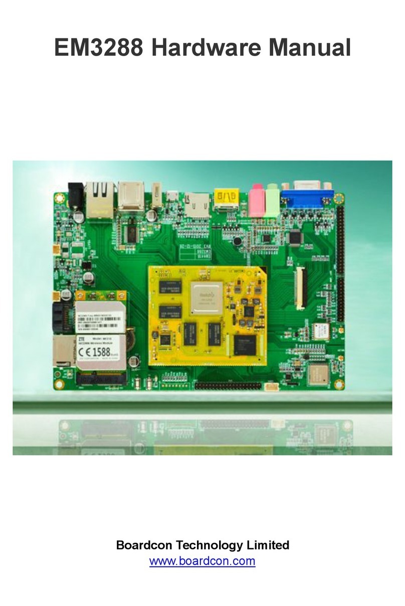
Boardcon EM-IMX8M-MINI User manual

EM-IMX8M-MINI Reference User Manual
V1.0
www.boardcon.com
Boardcon Embedded Design

1
Customize the embedded system based on YourIdea
1. Introduction
1.1. About this Manual
This manual is intended to provide the user with an overview of the board and benefits, complete
features specifications, and set up procedures. It contains important safety information as well.
1.2. Feedback and Update to this Manual
To help our customers make the most of our products, we are continually making additional and
updated resources available on the Boardcon website (www.boardcon.com , www.armdesigner.com).
These include manuals, application notes, programming examples, and updated software and
hardware. Check in periodically to see what’s new!
When we are prioritizing work on these updated resources, feedback from customers is the number
one influence, If you have questions, comments, or concerns about your product or project, please
no hesitate to contact us at support@armdesigner.com.
1.3. Limited Warranty
Boardcon warrants this product to be free of defects in material and workmanship for a period of one
year from date of buy. During this warranty period Boardcon will repair or replace the defective unit
in accordance with the following process:
A copy of the original invoice must be included when returning the defective unit to Boardcon. This
limited warranty does not cover damages resulting from lighting or other power surges, misuse,
abuse, abnormal conditions of operation, or attempts to alter or modify the function of the product.
This warranty is limited to the repair or replacement of the defective unit. In no event shall Boardcon
be liable or responsible for any loss or damages, including but not limited to any lost profits, incidental
or consequential damages, loss of business, or anticipatory profits arising from the use or inability
to use this product.
Repairs make after the expiration of the warranty period are subject to a repair charge and the cost
of return shipping. Please contact Boardcon to arrange for any repair service and to obtain repair
charge information.

2
Customize the embedded system based on YourIdea
Content
1 EM-IMX8M-MINI Introduction .........................................................................................................3
1.1 Summary..............................................................................................................................3
1.2 Processor Features ..............................................................................................................3
1.3 EM-IMX8M-MINI Specifications ...........................................................................................4
1.4 PCB Dimension....................................................................................................................5
1.5 Block Diagram......................................................................................................................6
1.6 Power Meter.........................................................................................................................6
1.7 CPU Introduction..................................................................................................................6
2 Peripherals Introduction .................................................................................................................8
2.1 Power ...................................................................................................................................8
2.2 RS485 ..................................................................................................................................9
2.3 CAN....................................................................................................................................10
2.4 Keys ...................................................................................................................................10
2.5 Audio ..................................................................................................................................10
2.6 UART..................................................................................................................................12
2.7 JTAG ..................................................................................................................................13
2.8 MIPI DSI.............................................................................................................................13
2.9 MIPI CSI.............................................................................................................................14
2.10 PCIe M.2 ..........................................................................................................................15
2.11 SD.....................................................................................................................................17
2.12 Infrared Receiver(U3).......................................................................................................17
2.13 USB(OTG/HOST).............................................................................................................17
2.14 Ethernet............................................................................................................................18
2.15 GPIO ................................................................................................................................19
2.16 WiFi & Bluetooth ..............................................................................................................20
3 Product Configurations .................................................................................................................21
Standard Contents ...................................................................................................................21

3
Customize the embedded system based on YourIdea
1 EM-IMX8M-MINI Introduction
1.1 Summary
The EM-IMX8M-MINI is based around the NXP i.MX8M Mini processor. It is tailor made for a wide
range of multimedia applications, featuring 2GB LPDDR4, 8GB eMMC, 2x USB 2.0 Host, powerful
network connectivity options including 4G, WiFi &BT. Robust multimedia features including 4K video
HEVC/H265/H264/VP9 decode with HDR, 2D/3D graphics acceleration, 16 audio channels (32bits),
MIPI-DSI, and 1080p encoder and decoder.
Together with MIPI CSI camera inputs, MIPI DSI display outputs, flexible audio interfaces and
comprehensive communication features, EM-IMX8M-MINI is ideal for Advanced graphics, machine
vision, and other multimedia applications.
1.2 Processor Features
Multicore Processing
⚫4x Cortex-A53 core platforms up to 1.8GHz per core
⚫32KB L1-I Cache/ 32 kB L1-D Cache
⚫512 kB L2 Cache
⚫1x Arm Cortex-M4 core up to 400MHz
⚫16 kB L1-I Cache/ 16 kB L2-D Cache
GPU
⚫3D GPU (1x shader, OpenGL®ES 2.0)
⚫2D GPU
Display Interface
⚫1x MIPI DSI (4-lane) with PHY
Video Playback
⚫1080p60 VP9 Profile 0, 2 (10-bit) decoder, HEVC/H.265 decoder, AVC/H.264 Baseline,
Main, High decoder, VP8 decoder
⚫1080p60 AVC/H.264 encoder, VP8 encoder
Audio
⚫5x SAI (12Tx + 16Rx external I2S lanes), 8ch PDM input
Camera Interface
⚫1x MIPI CSI (4-lane) with PHY
USB
⚫2x USB 2.0 OTG controllers with integrated PHY
PCIe
⚫1x PCIe 2.0 (1-lane) with L1 low power substate
Ethernet
⚫1x Gigabit Ethernet (MAC) with AVB and IEEE 1588, Energy Efficient Ethernet (EEE) for
low power

4
Customize the embedded system based on YourIdea
1.3 EM-IMX8M-MINI Specifications
Feature
Specifications
CPU
i.MX 8MQuad, 4x ARM Cortex-A53 @ 1.8 GHz
1 MB L2 cache
ARM Cortex-M4 @ 400 MHz
GPU
OpenGL ES1.1,2.0, OpenVG1.1
Memory
2GB LPDDR4
Storage
8GB eMMC flash
Power Management
ROHM BD71847
Power Input
DC 5V/3A
USB
1x USB 2.0 OTG, micro-USB connector
2x USB 2.0 Host, type-A connector
UART
1x RS232(COM1), 3x UARTs (J12, J13, J14)
Ethernet
Gigabit Ethernet port, RJ45 connector. Realtek RTL8211E
Audio
WM8960 audio codec. 3.5mm audio jack, 2x 2pin header for Speaker
Expand Audio
8bit RX and 8bit TX SAI interface, 40-pin header (J5)
SD
Micro SD socket, SD3.01
Display
MIPI-DSI, 4 data lanes, up to 1920 x 1080 @60Hz, 26-pin header (CON2)
RTC
Real time clock, powered by external battery
Power in
DC 5V/3A
Power
key
RS485
CAN
Reset
Power
ON/OFF
Speaker
Headphone
UART
JTAG
MIPI LCD
MIPI Camera
Optional
Debug
Cortex-M4
IR
Nano SIM
Micro SD
USB OTG
USB Host
Ethernet
RTC
GPIO
Audio card
UART
RS232
Boot mode
WiFi&Bluetooth 4G/SSD
Optional
Debug
Cortex-A7

5
Customize the embedded system based on YourIdea
JTAG
JTAG debug interface, 10-pin header
CAN
2-Pin connector (P4)
RS485
Compatible 9-bit data format, 3-pin connector (P3)
Buttons
Reset (SW2), Power (SW3), Boot Mode (SW4)
Expand interface
2x I2C, 1x SPI, 6x GPIO, 26-pin header (J11)
PCIe
Support USB2.0, PCIE2.1, UIM interface for SSD or 4G module
Camera
MIPI-CSI, 4 data lanes, 26-pin header (CON1)
WiFi&Bluetooth
802.11b/g/n WiFi, Bluetooth 4.0. AP6236 chipset
SIM
Nano SIM
Dimension
Baseboard - 102.3mm x 118.6mm; Core board – 67.6mm x 34.3 mm
1.4 PCB Dimension
118 6mm.
102.3mm

6
Customize the embedded system based on YourIdea
1.5 Block Diagram
1.6 Power Meter
Power
OS
Operation
Temperature
°C
Connected Devices
Electric
Current
(mA)
5V/3A
Linux4.14.98
28 °C
Power, debug port
375
Power, debug port, ethernet, 7-inch MIPI LCD,
SD card, 2 x U-disk
790
Power, debug port, ethernet, 7-inch MIPI LCD,
SD card, 2 x U-disk, Play audio
825
1.7 CPU Introduction
SOM-IMX8M-MINI specifications
Pin number – 200 pins
Dimension – 67.6mm x 34.3 mm
Layer – 6 Layers
Power supply – DC 5V
Connector –SO-DIMM200 edge connector
Application – Advanced graphics, machine vision, and other media applications
On SOM Board
I2S DAC
WiFi/BT
802.11b/g/n
M.2 NGFF
KEY-E:WiFi/BT...
LANE x4
MIPI DSI
mini-SAS CN
MIPI CSI
mini-SAS CN
GPIO/UART
EXPCN
LPDDR4
DRAM
x32 bits
eMMC 5.1 x8 bits
GPIO/SAI/I2C...GPIO/UART...
Audio Card
SAI/GPIO/I2C...
MicroSD
Button
ONOFF
x4 bits
SDIO
SDIO
ONOFF/GPIO
JTAGMIPI DSI MIPI CSI
SDIO/UART/PCM
PCIe
SAI
SAI2C/I
ARM CORTEX 4x A53 + M4
2.4/5GHz
2.4/5GHz
POWERPMIC
i.MX8M Mini
LPDDR4
JTAG
10 PIN Header
JTAG
USB TYPE-C
USB 2.0 OTG
DRP x2
USB OTG
Infrared
/ LED
GPIO/PWM
Giga Ethernet
I2C
I2C CN
I2C/RST
SD3.0
PWM
DBG UART
LANE x4
GPIO/UART I2C
Button
Reset
QSPI Nor x4 bits
RJ45
RGMII
UART
RGMII
x2 UART(A53/M4)

7
Customize the embedded system based on YourIdea
Pin Definition
Pin
Signal
Pin
Signal
Pin
Signal
Pin
Signal
1
GND
101
GND
2
GND
102
SD2_DATA1
3
GND
103
PCIE_RXP
4
GND
104
SD2_DATA2
5
GND
105
PCIE_RXN
6
GND
106
SD2_DATA3
7
VSYS_5V
107
GND
8
VSYS_5V
108
SD1_STROBE
9
VSYS_5V
109
CSI_DP3
10
VSYS_5V
110
BOOT_MODE1
11
VSYS_5V
111
CSI_DN3
12
VSYS_5V
112
BOOT_MODE0
13
GND
113
GND
14
GND
114
JTAG_TMS
15
GND
115
CSI_DP2
16
GND
116
JTAG_TDO
17
VDD_1V8
117
CSI_DN2
18
VDD_1V8
118
JTAG_TDI
19
VDD_1V8
119
GND
20
VDD_1V8
120
JTAG_TCK
21
GND
121
CSI_CKP
22
GND
122
JTAG_nTRST
23
VDD_3V3
123
CSI_CKN
24
VDD_3V3
124
CLKOUT1
25
VDD_3V3
125
GND
26
M.2_32K_OUT
126
CLKOUT2
27
SAI1_TXD7
127
CSI_DP1
28
SAI1_TXD6
128
CLKIN1
29
SAI1_TXD5
129
CSI_DN1
30
SAI1_TXD4
130
CLKIN2
31
SAI1_TXD3
131
GND
32
SAI1_TXD2
132
ONOFF
33
SAI1_TXD1
133
CSI_DP0
34
SAI1_TXD0
134
USB2_VBUS
35
GND
135
CSI_DN0
36
SAI1_TXC
136
USB1_VBUS
37
SAI1_RXC
137
GND
38
SAI1_TXFS
138
USB2_ID
39
SAI1_RXFS
139
DSI_DP3
40
GND
140
USB1_ID
41
SAI1_RXD7
141
DSI_DN3
42
SAI1_RXD6
142
UART4_TXD
43
SAI1_RXD5
143
GND
44
SAI1_RXD4
144
UART4_RXD
45
SAI1_RXD3
145
DSI_DP2
46
SAI1_RXD2
146
UART1_RTS
47
SAI1_RXD1
147
DSI_DN2
48
SAI1_RXD0
148
UART1_CTS
49
SAI5_RXFS
149
GND
50
GND
150
UART2_TXD
1199
2
200

8
Customize the embedded system based on YourIdea
51
DM_CLK
151
DSI_CKP
52
PDM_DATA2
152
UART2_RXD
53
SAI5_MCLK
153
DSI_CKN
54
PDM_DATA3
154
UART1_TXD
55
PDM_DATA1
155
GND
56
GND
156
UART1_RXD
57
GND
157
DSI_DP1
58
PDM_DATA0
158
I2C4_SCL
59
SYS_nRST
159
DSI_DN1
60
SAI1_MCLK
160
I2C4_SDA
61
GND
161
GND
62
GND
162
I2C3_SCL
63
ENET_TXC
163
DSI_DP0
64
ENET_TX_CTL
164
I2C3_SDA
65
GND
165
DSI_DN0
66
ENET_TD0
166
I2C2_SCL
67
ENET_TD1
167
GND
68
ENET_TD2
168
I2C2_SDA
69
ENET_TD3
169
UART3_RXD
70
ENET_RX_CTL
170
ECSPI2_MOSI
71
ENET_RXC
171
UART3_TXD
72
GND
172
ECSPI2_MISO
73
ENET_RD0
173
UART3_CTS
74
ENET_RD1
174
ECSPI2_SCLK
Pin
Signal
Pin
Signal
Pin
Signal
Pin
Signal
75
PMIC_ON_REQ
175
UART3_RTS
76
ENET_RD2
176
ECSPI2_SS0
77
GND
177
GND
78
ENET_RD3
178
SAI3_TXD
79
USB2_DP
179
SAI3_TXC
80
ENET_MDC
180
SAI3_TXFS
81
USB2_DN
181
SAI3_RXD
82
ENET_MDIO
182
SAI3_MCLK
83
GND
183
SAI3_RXC
84
GND
184
GPIO1_IO13
85
USB1_DP
185
SAI3_RXFS
86
GND
186
GPIO1_IO10
87
USB1_DN
187
GPIO1_IO15
88
SD2_nCD
188
GPIO1_IO12
89
GND
189
GPIO1_IO14
90
SD2_WP
190
GPIO1_IO08
91
PCIE_CLKP
191
GPIO1_IO05
92
SD2_CMD
192
GPIO1_IO11
93
PCIE_CLKN
193
GPIO1_IO07
94
SD2_CLK
194
GPIO1_IO01
95
GND
195
GPIO1_IO09
96
SD2_nRST
196
SPDIF_EXT_CLK
97
PCIE_TXP
197
GPIO1_IO06
98
GND
198
SPDIF_RX
99
PCIE_TXN
199
GND
100
SD2_DATA0
200
SPDIF_TX
2 Peripherals Introduction
2.1 Power
⚫5V Power (P1)
Universal 5V/3A power supply with 2P2T slide switch.
Note: Over-voltage protection is designed to withstand up to +5.5V.
1
2
3

9
Customize the embedded system based on YourIdea
P1
Pin
Signal
Description
Pin
Signal
Description
1
5VIN
Main power supply. DC 5V power in
2
GND
Ground
3
GND
Ground
SW1
Pin
Signal
Description
Pin
Signal
Description
1
GND
Ground
2
NC
Not connect/ Ground
3
GND
Ground
4
DC_SW_CTL
DC 5V control
5
NC
Not connect/ Ground
6
GND
Ground
7
DC_SW_CTL
DC 5V control
8
GND
Ground
⚫RTC (BT1)
The backup battery (3V) is used to ensure the RTC (frequency 32.768KHz) is still able to work after
power off. Cell model: CR1220.
Pin
Signal
Description
Pin
Signal
Description
1
VDD_3V3
3V battery
2
GND
Ground
2.2 RS485
SN75176B Differential bus transceiver.
⚫Bidirectional Transceivers
⚫± 200mV Receiver Input Sensitivity
⚫50mV Type Receiver Input Hysteresis
P9
Pin
Signal
Description
Pin
Signal
Description
1
RS485_A
RS-485 Data Line
2
RS485_B
RS-485 Data Line
3
GND
Ground
1248
57
3
2
1

10
Customize the embedded system based on YourIdea
2.3 CAN
MCP2551 transceiver.
⚫Supports 1 Mb/s operation
⚫Low current standby operation
⚫High noise immunity due to differential bus implementation
Pin
Signal
Description
Pin
Signal
Description
1
CANL
CAN Low-Level Voltage I/O
2
CANH
CAN High-Level Voltage I/O
2.4 Keys
SW2/SW3 is Tact switch used for Power/Reset.
Key
Signal
Description
Key
Signal
Description
SW2
ONOFF
CPU ON/OFF
SW3
SYS_nRST
Reset
SW4 is a DIP Switch for the selection of BOOT mode.
SW4
Boot Mode
1
2
Download
OFF
OFF
eMMC Boot
ON
ON
2.5 Audio
The Audio Codec WM8960 supports stereo audio ADC/DAC. EM-IMX8M-MINI features a SAI
(synchronous audio interface) with 8 TX and 8 RX lanes.
12
12
= ON
ON
12
ON
12

11
Customize the embedded system based on YourIdea
J8 (Headphone)
Pin
Signal
Description
Pin
Signal
Description
1
GND
Ground
2
HPOUTR
Headphone right
channel output
3
HPOUTL
Headphone left channel
output
4
HP_DETEC
Headphone detect
5
MIC_RAW
Microphone input
J6 (Speaker)
Pin
Signal
Description
Pin
Signal
Description
1
SPK_LN
Speaker left channel -
2
SPK_LP
Speaker left channel +
J7 (Speaker)
Pin
Signal
Description
Pin
Signal
Description
1
SPK_RN
Speaker right channel -
2
SPK_RP
Speaker right channel +
The Headphone and speaker sync output audio.
Audio card (J5)
Pin
Signal
Description
Pin
Signal
Description
1
5V_EXT
5V power supply
2
VEXT_3V3
3.3V power supply
3
VEXT_3V3
3.3V power supply
4
SAI1_MCLK
SAT master clock
5
GND
Ground
6
SAI1_TXC
Transmit Bit Clock
7
GND
Ground
8
SAI1_TXFS
Transmit Frame Sync
9
SAI1_TXD0
Transmit Data
10
SAI1_TXD1
Transmit Data
11
SAI1_TXD2
Transmit Data
12
SAI1_TXD3
Transmit Data
3
1
4
2
5
12
1 3 57 9 11 13 15 17 19 21 23 25
2 4 6 8 10 12 14 16 18 20 22 24 26
21 23 25 27 29 31 33 35 37 39
28 30 32 34 36 38 40
GND
I2C
SPDIF
GPIO
SAI
Power supply

12
Customize the embedded system based on YourIdea
13
SAI1_TXD4
Transmit Data
14
SAI1_TXD5
Transmit Data
15
SAI1_TXD6
Transmit Data
16
SAI1_TXD7
Transmit Data
17
GND
Ground
18
SAI1_RXC
Receive Bit Clock.
19
SAI1_RXFS
Receive Frame Sync
20
SAI1_RXD0
Receive Data
21
SAI1_RXD1
Receive Data
22
SAI1_RXD2
Receive Data
23
SAI1_RXD3
Receive Data
24
SAI1_RXD4
Receive Data
25
SAI1_RXD5
Receive Data
26
SAI1_RXD6
Receive Data
27
SAI1_RXD7
Receive Data
28
GND
Ground
29
GND
Ground
30
EXP_IO4
External IO
31
EXP_IO5
External IO
32
GND
Ground
33
SPDIF_EXT_
CLK
SPDIF External Clock
34
SPDIF_TX
SPDIF Transmit
35
SPDIF_RX
SPDIF Receive
36
I2C3_SCL
I2C Serial Clock
37
I2C3_SDA
I2C Serial Data
38
GND
Ground
39
GND
Ground
40
GND
Ground
2.6 UART
• Up to 6 UARTS
• 64-Bytes Transmit and receive data FIFOs for all UART
• Compliant with industry-standard 16550 UARTs
• Support Infrared Data Association(IrDA) 1.0 SIRR
J12/J13/J14/COM1(DB9) are RS232 signal. The signal of J14 is converted by a USB-to-Dual-
UART Bridge Controller CP2105.
COM1
Pin
Signal
Description
Pin
Signal
Description
1
NC
Not connect
2
RS232_RX3
Receive Data
3
RS232_TX3
Transmit Data
4
NC
Not connect
5
GND
Ground
6
NC
Not connect
7
RS232_RTS
Request to send
8
RS232_CTS
Clear to send
9
NC
Not connect
J12 (pin header, debug for Cortex-M4)
Pin
Signal
Description
Pin
Signal
Description
6
1 2 345
7 8 9
2 1
3
4

13
Customize the embedded system based on YourIdea
1
VEXT_3V3
3.3V power supply
2
UART2_RXD
Receive Data
3
UART2_TXD
Transmit Data
4
GND
Ground
J13 (pin header, debug for Cortex-A7)
Pin
Signal
Description
Pin
Signal
Description
1
VEXT_3V3
3.3V power supply
2
UART4_RXD
Receive Data
3
UART4_TXD
Transmit Data
4
GND
Ground
J14 (pin header)
Pin
Signal
Description
Pin
Signal
Description
1
VEXT_3V3
3.3V power supply
2
U_UART1_RXD
Receive Data
3
U_UART1_TXD
Transmit Data
4
GND
Ground
2.7 JTAG
There is a JTAG (a serial bus protocol usually used for test purposes) on the chip. IMX8M-Mini
Supports 2 x 5-pins (JTAG) interface.
Pin
Signal
Description
Pin
Signal
Description
1
VDD_3V3
3.3V power supply
2
JTAG_TMS
Test Mode Select
3
GND
Ground
4
JTAG_TCK
Test Clock
5
GND
Ground
6
JTAG_TDO
Test Data Out
7
NC
NC
8
JTAG_TDI
Test Data In
9
NC/JTAG_nT
RST
NC/Test Reset
10
nRST
Reset
2.8 MIPI DSI
Support up to 1080p@60Hz display through a 4-lane MIPI DSI.
Features
⚫Compliant to MIPI-DSI standard v1.1
⚫Support up to 4 data lanes
⚫Support 80Mbps - 1.5Gbps data rate in high speed operation
⚫Support 10Mbps data rate in low power operation
13 5 7 9
2 4 6 8 10

14
Customize the embedded system based on YourIdea
Pin
Signal
Description
Pin
Signal
Description
1
MIPI_5V0
5V power supply
2
MIPI_5V0
5V power supply
3
GND
Ground
4
GND
Ground
5
MIPI_3V3
3.3V power supply
6
MIPI_3V3
3.3V power supply
7
MIPI_1V8
1.8V power supply
8
GND
Ground
9
NC
Not connect
10
DSI_BL_PWM
Backlight
11
DSI_EN
DSI enable
12
I2C3_SCL
I2C serial clock
13
I2C3_SDA
I2c serial date
14
DSI_RST
Touch screen reset
15
DSI_TS_nINT
Touch screen interrupt
16
GND
Ground
17
DSI_DN0
DSI data -
18
DSI_DP0
DSI data +
19
DSI_DN1
DSI data -
20
DSI_DP1
DSI data +
21
DSI_CKN
DSI clock -
22
DSI_CKP
DSI clock +
23
DSI_DN2
DSI data -
24
DSI_DP2
DSI data +
25
DSI_DN3
DSI data -
26
DSI_DP3
DSI data +
2.9 MIPI CSI
The CSI is a simple camera interface. It captures the MIPI CSI input and saves the pixels into
memory. The chip supports one 4-lane MIPI CSI2 camera input.
Features
⚫Configurable interface logic to support most commonly available CMOS sensors
⚫8-bit / 16-bit / 24-bit data port for YCbCr, YUV, or RGB data input
⚫Full control of 8-bit/pixel, 10-bit/pixel or 16-bit / pixel data format to 64-bit receive
⚫Compliant to MIPI-CSI2 standard
⚫Support up to 4 data lanes
⚫Support 80Mbps - 1.5Gbps data rate in high speed operation
⚫Support 10Mbps data rate in low power operation
⚫Support 5M pixel at 15 fps, 1080p60, 720p60, VGA at 60 fps
Pin
Signal
Description
Pin
Signal
Description
13 5 7 9 11 13 15 17 19 21 23 25
24 6 8 10 12 14 16 18 20 22 24 26
GND
I2C
DSI
Power supply
NC
GND
I2C
CSI
Power supply
NC
13 5 7 9 11 13 15 17 19 21 23 25
24 6 8 10 12 14 16 18 20 22 24 26

15
Customize the embedded system based on YourIdea
1
MIPI_5V0
5V power supply
2
MIPI_5V0
5V power supply
3
GND
Ground
4
GND
Ground
5
MIPI_3V3
3.3V power supply
6
MIPI_3V3
3.3V power supply
7
MIPI_1V8
1.8V power supply
8
GND
Ground
9
CAMERA_PWDN
Camera Power down
10
CAMERA_RST
Camera Reset
11
CAMERA_CLK
Camera clock
12
I2C2_SCL_1V8
I2C serial clock
13
I2C2_SDA_1V8
I2C serial date
14
NC
Not connect
15
NC
Not connect
16
GND
Ground
17
CSI_CKN
MIPI clock -
18
CSI_CKP
MIPI clock +
19
CSI_DN0
Negative
Transmission Data of
Pixel0
20
CSI_DP0
Positive
Transmission Data
of Pixel0
21
CSI_DN1
Negative
Transmission Data of
Pixel1
22
CSI_DP1
Positive
Transmission Data
of Pixel1
23
CSI_DN2
Negative
Transmission Data of
Pixel2
24
CSI_DP2
Positive
Transmission Data
of Pixel2
25
CSI_DN3
Negative
Transmission Data of
Pixel3
26
CSI_DP3
Positive
Transmission Data
of Pixel3
2.10 PCIe M.2
EM-IMX8M-Mini adopts the PCIe M.2 socket (NGFF_M.2 B-KEY_8.5H).
PCIe (for 4G/SSD module)
Pin
Signal
Description
Pin
Signal
Description
1
CONFIG_3
Module
Configuration
2
VPCIe_3V3
3.3V power supply
3
GND
Ground
4
VPCIe_3V3
3.3V power supply
5
GND
Ground
6
Full_CPO
Full card power off
7
M2_USB_DP
USB Data +
8
PCIe_nDIS
PCIe disable
9
M2_USB_DN
USB Data -
10
TP21
Test point
11
GND
Ground
20
TP17
Test point
21
CONFIG_0
Module
Configuration
22
TP18
Test point
23
TP23
Test point
24
TP19
Test point
2 10 20 74
1 11 21 75

16
Customize the embedded system based on YourIdea
25
TP24
Test point
26
TP22
Test point
27
GND
Ground
28
TP20
Test point
29
NC
Not connect
30
SIM_RST
SIM reset signal
31
NC
Not connect
32
SIM_CLK
SIM clock signal
33
GND
Ground
34
SIM_DATA
SIM data signal.
35
NC
Not connect
36
SIM_VCC
Power for the SIM.
37
NC
Not connect
38
DEVSLP
Device Sleep
39
GND
Ground
40
TP12
Test point
41
PCIE_RXN
PCIe RX -
42
TP13
Test point
43
PCIE_RXP
PCIe RX +
44
TP14
Test point
45
GND
Ground
46
TP15
Test point
47
PCIE_TXN
PCIe TX -
48
TP16
Test point
49
PCIE_TXP
PCIe TX +
50
PCIe_nRST
PCIe reset
51
GND
Ground
52
PCIe_nCLKR
EQ_DEV
Clock Request
53
REF_CLKN_CN
PCIe Reference
Clock signals -
54
PCIe_nWAKE
PCIe PME Wake
55
REF_CLKP_CN
PCIe Reference
Clock signals +
56
NC
Not connect
57
GND
Ground
58
NC
Not connect
59
NC
Not connect
60
NC
Not connect
61
NC
Not connect
62
NC
Not connect
63
NC
Not connect
64
NC
Not connect
65
NC
Not connect
66
SIM_DET
Detect the SIM
insertion/removal
67
M_2_RESET
M.2 module Reset
68
M.2_32K_OU
T
Suspend Clock (32KHz)
69
CONFIG_1
Module
Configuration
70
VPCIe_3V3
3.3V power supply
71
GND
Ground
72
VPCIe_3V3
3.3V power supply
73
GND
Ground
74
VPCIe_3V3
3.3V power supply
75
CONFIG_2
Module
Configuration
Nano SIM Slot
Pin
Signal
Description
Pin
Signal
Description
1
SIM_CLK
Clock signal
2
SIM_DATA
Send/Receiver data
3
SIM_RST
Reset signal
4
SIM_VCC
Power supply
5
SIM_VCC
Power supply
6
GND
Ground
7
1

17
Customize the embedded system based on YourIdea
7
GND
Ground
2.11 SD
The Micro SD card is used as an external storage device. The MMC controller interface supports up
to 4-bit transfer modes.
Pin
Signal
Description
Pin
Signal
Description
1
SD2_DATA2
SD2 Data Bit
2
SD2_DATA3
SD2 Data Bit
3
SD2_CMD
SD2 Command Signal
4
VSD_3V3
3.3V power supply
5
SD2_CLK
SD2 Clock
6
GND
Ground
7
SD2_DATA0
SD2 Data Bit
8
SD2_DATA1
SD2 Data Bit
9
SD2_DET
SD Detect
2.12 Infrared Receiver(U3)
IRM-V538T Remote Receiver Sensor, 38.0KHz
Pin
Signal
Description
Pin
Signal
Description
1
IR_CAP
IR in
2
VDD_3V3
3.3V Power supply
3
GND
Ground
2.13 USB(OTG/HOST)
The USB 2.0 OTG is a Micro USB port, used for download image.
USB OTG
Pin
Signal
Description
Pin
Signal
Description
1
VBUS1
BUS1 Voltage
2
USB1_DN
OTG data -
3
USB1_DP
OTG data+
4
USB1_ID
OTG ID indicator
5
GND
Ground
9
1
1
5

18
Customize the embedded system based on YourIdea
EM-IMX8M-MINI features 2x USB 2.0 Host. It supports high-speed (480Mbps), full-speed (12Mbps)
and low-speed (1.5Mbps) mode.
USB HOST (J3)
Pin
Signal
Description
Pin
Signal
Description
1
VCC_5V
USB Power. DC 5V
2
HUB_USB3_DM
USB data-
3
HUB_USB3_DP
USB Data+
4
GND
Ground
5
GND
Ground
6
GND
Ground
USB HOST (J4)
Pin
Signal
Description
Pin
Signal
Description
1
VCC_5V
USB Power. DC 5V
2
HUB_USB2_DM
USB data-
3
HUB_USB2_DP
USB Data+
4
GND
Ground
5
GND
Ground
6
GND
Ground
2.14 Ethernet
EM-IMX8M-MINI adopts RTL8211E as the Ethernet chip. RJ45 connector (offset).
Feature
⚫Implements the full 802.3 specification
⚫Dynamically configurable to support 10/100/1000-Mbit/s operation
⚫Supports 10/100 Mbit/s full-duplex and configurable half-duplex operation
⚫Supports gigabit full-duplex operation
JP2 (RJ45)
Pin
Signal
Description
Pin
Signal
Description
1
DA+
Bi-directional
transmit/receive pair A
2
DA-
Bi-directional
transmit/receive pair A
3
DB+
Bi-directional
transmit/receive pair B
4
DC+
Bi-directional
transmit/receive pair C
5
DC-
Bi-directional
transmit/receive pair C
6
DB-
Bi-directional
transmit/receive pair B
7
DD+
Bi-directional
8
DD-
Bi-directional
1
4
5
6
1
2
7
8
13
12

19
Customize the embedded system based on YourIdea
transmit/receive pair D
transmit/receive pair D
9
GND
Ground
10
GND
Ground
11
SPEED
Network speed
12
GND
Ground
13
VEXT_3V3
DC 3.3V power supply
14
LINK
Link activity
2.15 GPIO
The i.MX8M Mini Dev Board provides access to several peripheral interfaces through the 26-pin
expansion header (J11), including GPIO, I2C, UART, and SPI.
Note
If UART1_RTS and UART1_CTS used in WiFi module, then can't be used in motherboard.
If WiFi module is used, the UART1_RXD and UART1_TXD pins only can be used for GPIOs.
Pin
Signal
Description
Pin
Signal
Description
1
VEXT_3V3
3.3V power supply
2
VDD_5V
5V power supply
3
VEXT_3V3
3.3V power supply
4
VDD_5V
5V power supply
5
I2C3_SDA
I2C serial data
6
GND
Ground
7
I2C3_SCL
I2C serial clock
8
GND
Ground
9
GND
Ground
10
ENET_nRST/
GPIO5_IO23/
UART1_TXD
Ethernet reset/
GPIO/UART transmit
11
I2C4_SDA
I2C serial data
12
GPIO5_IO22/
UART1_RXD
GPIO/UART receive
13
I2C4_SCL
I2C serial clock
14
UART1_RTS
Request to send
15
NC/ECSPI2_M
OSI
NC/Master output,
Slave input
16
UART1_CTS
Clear to send
17
NC/ECSPI2_MI
SO
NC/Master input, Slave
output
18
SAI5_RXD0
SAI receive
19
NC/ECSPI2_SC
LK
NC/SPI Serial clock
20
EXP_IO6
GPIO
21
NC/ECSPI2_SS
0
NC/SPI slave select
22
EXP_IO7
GPIO
23
GND
Ground
24
EXP_IO9
GPIO
25
GND
Ground
26
EXP_IO8
GPIO
13 5 7 9 11 13 15 17 19 21 23 25
24 6 8 10 12 14 16 18 20 22 24 26
GND
I2C
SPI
GPIO
UART
SAI
Power supply
Table of contents
Other Boardcon Motherboard manuals
