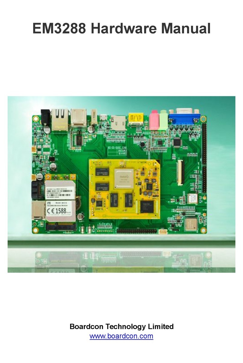
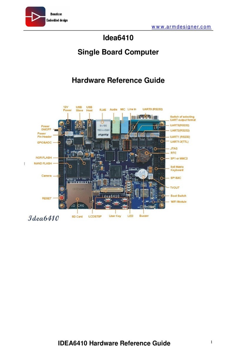
Boardcon EMA40i User manual

EMA40i Reference User Manual
V1.201909
www.boardcon.com
Boardcon Embedded Design

1
Customize the embedded system based on YourIdea
1. Introduction
1.1. About this Manual
This manual is intended to provide the user with an overview of the board and benefits, complete
features specifications, and set up procedures. It contains important safety information as well.
1.2. Feedback and Update to this Manual
To help our customers make the most of our products, we are continually making additional and
updated resources available on the Boardcon website
(www.boardcon.com ,www.armdesigner.com).
These include manuals, application notes, programming examples, and updated software and
hardware. Check in periodically to see what’s new!
When we are prioritizing work on these updated resources, feedback from customers is the number
one influence, If you have questions, comments, or concerns about your product or project, please
no hesitate to contact us at support@armdesigner.com.
1.3. Limited Warranty
Boardcon warrants this product to be free of defects in material and workmanship for a period of one
year from date of buy. During this warranty period Boardcon will repair or replace the defective unit
in accordance with the following process:
A copy of the original invoice must be included when returning the defective unit to Boardcon. This
limited warranty does not cover damages resulting from lighting or other power surges, misuse,
abuse, abnormal conditions of operation, or attempts to alter or modify the function of the product.
This warranty is limited to the repair or replacement of the defective unit. In no event shall Boardcon
be liable or responsible for any loss or damages, including but not limited to any lost profits, incidental
or consequential damages, loss of business, or anticipatory profits arising from the use or inability
to use this product.
Repairs make after the expiration of the warranty period are subject to a repair charge and the cost
of return shipping. Please contact Boardcon to arrange for any repair service and to obtain repair
charge information.

2
Customize the embedded system based on YourIdea
Content
1 EMA40i Introduction .......................................................................................................................3
1.1 Summary..............................................................................................................................3
1.2 A40i Features .......................................................................................................................3
1.3 EMA40i Specifications .........................................................................................................4
1.4 PCB Dimension ....................................................................................................................5
1.5 Block Diagram ......................................................................................................................6
1.6 Power Meter .........................................................................................................................7
1.7 CPU Introduction ..................................................................................................................8
2 Peripherals Introduction ...............................................................................................................17
2.1 Power .................................................................................................................................17
2.2 HDMI ..................................................................................................................................18
2.3 USB Host ...........................................................................................................................18
2.4 USB OTG ...........................................................................................................................19
2.5 AV_IN .................................................................................................................................19
2.6 UART..................................................................................................................................20
2.7 Ethernet..............................................................................................................................21
2.8 Micro SD ............................................................................................................................22
2.9 Audio (Headphone/Speaker)..............................................................................................23
2.10 LCD(MIPI/RGB/LVDS) .....................................................................................................23
2.11 RS485...............................................................................................................................27
2.12 CAN..................................................................................................................................27
2.13 GPIO&Control ..................................................................................................................28
2.14 4G Module........................................................................................................................29
2.15 Camera ............................................................................................................................30
2.16 GPS..................................................................................................................................31
2.17 WiFi&Bluetooth ................................................................................................................32
2.18 SATA ................................................................................................................................33
2.19 Keys .................................................................................................................................35
3 Product Configurations .................................................................................................................35
3.1 Standard Contents .............................................................................................................35
3.2 Optional Parts ....................................................................................................................35

3
Customize the embedded system based on YourIdea
1 EMA40i Introduction
1.1 Summary
EMA40i is a single board computer featuring an Allwinner A40i Processor, comes with 1GB DDR3
RAM, 8GB eMMC, and other rich interfaces specifically designed for intelligent industrial control
applications such as industrial control, communications and measurement.
EMA40i provides a standard Gigabit Ethernet port and a 10-pin Extra GbE port. Supports HDMI 1.4,
RGB, MIPI DSI and dual-LVDS output. The SBC is equipped with a microSD slot and a M.2 slot with
NAME SSD support. A mini-PCIe slot supports 4G module and is accompanied by a Nano-SIM slot.
Other features include 2x dual-USB 2.0 host ports, USB2.0 OTG, RS232 DB9 port, 4x 4-pin headers
for RS232, UART(TTL) and USB host.
EMA40i is equipped with WiFi 802.11ac and Bluetooth 4.0, as well as optional support for GPS, 4G
LTE connectivity.
1.2 A40i Features
⚫CPU
Quad-core ARM Cortex-A7 CPU Architecture, the most power efficient CPU core ARM’s ever
developed.
⚫GPU
Mali400 MP2
⚫Video Engine
Supports mainstream high-definition video decoding including H.264, H.263, MPEG1/2/4, xvid,
Sorenson Spark, VP6/8, AVS/AVS+, WMV7, WMV8 by 1080p@60fps. In the aspect of video
encoding, the A40i supports 1080p@45fps H.264 encoding ability.
⚫Camera
Supports dual COMS sensor parallel interfaces and 4-channel TVIN, which can easily finish multi
channel video recording.
⚫Display
Content can be display on 4-lane MIPI DSI display, or RGB panel, or LVDS panel. TV-out on HDMI
V1.4 is also supported.
⚫Audio
Integrated audio codec with 24 bit/192kHz DAC playback, and supports I2S/PCM interface for
Connecting to an external audio codec. I2C/PCM interface includes eight channels of TDM with
sampling precision up to 32 bit/192kHz.
⚫Memory
Supports external memory interface to NAND Flash, SD/EMMC, Nor Flash and SDRAM port.
SDRAM. port can be configured to support LPDDR2, LPDDR3, DDR2, DDR3, and DDR3L.

4
Customize the embedded system based on YourIdea
1.3 EMA40i Specifications
Feature
Specifications
CPU
Quad-core ARM Cortex-A7 MPCore Processor
GPU
· Mali400 MP2 GPU
· Support OpenGL ES 2.0 / OpenVG 1.1 standard
Memory
1GB DDR3
iNAND
8GB eMMC
Power
DC 5V or 3.7V Li-Battery
Ethernet
1000M Ethernet (RTL8211E), RJ45/10-pin header interface
UART
5x UARTs, include 2x RS232 (DB9&4-pin header), 2x TTL(4-pin headers),
1x UART for Debug
TV-IN
4-ch TV in.
1-ch via RCA
3-ch via 4-pin header
USB
4 Channel x USB2.0 Host (2x dual-USB Host, 1x 4-pin header),
1x USB2.0 OTG
HDMI
HDMI 1.4
CAN
1x 2-pin header
RS485
1x 3-pin header
SD
Micro SD slot
COM2
(DB9)
RS232
UART7
TV_IN
USB Host x5
HDMI
Power_in
DC5V/3A
DC_5V
Li-battery
WiFi&BT
GPS
M.2 SATA
CAN
RS485
UART4
RGB_LCD
Dual-LVDS
Camera
MIPI_LCD
Control
Debug
Speaker
Headphone
PCIE(4G)
Nano SIM
Micro SD
USB OTG
Recover
Extra Ethernet
Ethernet
User key
Power
Reset
TV_IN*3
RTC
GPIO
optional
optional
optional

5
Customize the embedded system based on YourIdea
Audio
Support Audio I/O.
1x 3.5mm jack for headphone;
1x 2-pin header for Speaker.
LCD
1x 40pin Dual-channel LVDS;
1x 40pin RGB;
1x MIPI DSI
RTC
3V battery, CR1220
WiFi&BT
Wireless-2.4GHz IEEE 802.11b/g/n, Bluetooth4.0
SATA(optional)
M.2 slot. NVME SSD
4G(optional)
52pins MINI PCI-E Socket
GPS(optional)
Ublox 7 GPS Chipset
Camera(optional)
20-pin header
Others
20-pin GPIO, 8-pin control
Dimension
140mm x 100mm
1.4 PCB Dimension

6
Customize the embedded system based on YourIdea
1.5 Block Diagram
A40i Block Diagram
Display In
Display Out
MIPI DSI(4 lane)
1080p@60fps
LVDS
1080p@60fps
1080p@60fps
Video Decoder
1080p@60fps
32-bit
DDR3/DDR3L
8-bit NDFC
64-bit ECC
SD3.0/
eMMC5.0
System
CCU
GIC
DMA
Timer
PWM
Connectivity
USB2.0 OTG
TWI x5
SPI x4
UART x8
EMAC
GMAC
DE2.0
Crypto Engine
CSI x2
1080p@30fps
720p@30fps
Video Engine
USB HOST x2
Video Encoder
1080p@45fps
SDIO
TVIN x4
HDMI
1080P@60fps
TVOUT x4
SATA
PS2
TSC x2
KEYADC
Keypad
SMC
RTP
CIR
SID
Thermal Sensor
RTC
Memory
L2 cache
512KB
Audio Codec I2S/PCMx2 AC97 OWA OUT
Audio
ARM Cortex-A7 x4
A7
I cache
32KB
D cache
32KB
NEON
SIMD
Thumb-2
/FPU
Mali400 MP2
GPU
RGB

7
Customize the embedded system based on YourIdea
EMA40I Block Diagram
1.6 Power Meter
Power
OS
Operation
Temperature
°C
Connected Devices
Electric
Current
(mA)
5V@3A
Android7.1.1
Normal
5V power, serial cable
300
5V power, serial cable, 10.1’’ LVDS
710
5V power, serial cable, 10.1’’ LVDS, ethernet, 4x
USB, HDMI, SD, 4G, WIFI, GPS. Play 4K video
1140
5V@3A
Linux 3.10
Normal
5V power, serial cable
430
5V power, serial cable, 10.1’’ LVDS
870
5V power, serial cable, 10.1’’ LVDS, ethernet, 4x
USB, HDMI, SD, 4G, WIFI, GPS. Play 4K video
1300
32Gb eMMC
iNAND
1Gb RJ45
MIC
TF-Card
LVDS LCD
HP
AMP
UART3/SDIO0 SATA
Micro
SD1
EG8305
HPOUT/MIC
LVDS USB2
SSD
3G/4G
MPCI-E Socket
SDIO
4Gb: K4B4G1646E-BCM0
Digital Camera
USB1 USB0
DownloadOTG-USB
RGMII
B2B
B2B
1000 Mb netEther
parallel-CSI
1T1R WIFI/BT
AXP221S
SIM
Socket
DRAM
2x16bits
AP6236 Module
DDR3L
POWER
PMU
2.4 GHz <72.2Mbps
RTL8211E
A40I
C iM-A40
M.2 KEY-M
I2S2
SPEAKER
PJ327E
USB_HUB
GL850G
4xUSB host
USB-A
RGMII twisted pair
RS232
TVIN
Analog Camera 4 lanes DSI
MIPI-DSI TMDS
HDMI OUT
RBG LCD
24bit RGB
RS485
UART7 CAN XRX/T
CAN
UART6
GPS
UART4

8
Customize the embedded system based on YourIdea
1.7 CPU Introduction
CM-A40I specifications
Pin number – 196pins
Dimension – 45 x 58mm
Layer – 8 Layers, complying with EMS/EMI
Preinstalled OS – Linux3.10 or Android7.1
Power supply – DC 5V or 3.7V Battery
Application – Industrial control, communications and measurement, etc.
CM-A40I Pin Definition
Pin
Signal
Description
Alternate
functions
IO Voltage
1
KEYADC1
6bit ADC channel1
3.3V
2
KEYADC0
6bit ADC channel0
3.3V
3
FEL
Boot mode select:
Low: download from USB,
High: fast boot
3.3V
4
PD26/
LCD0_HSYNC
LCD0 horizontal sync
GPIOD26/
SMC_SLK
3.3V
5
PD27/
LCD0_VSYNC
LCD0 vertical sync
GPIOD27/
SMC_SDA
3.3V
6
USB-DP2
USB2 data +
3.3V
7
USB-DM2
USB2 data -
3.3V
8
USB-DP1
USB1 data +
3.3V
9
USB-DM1
USB1 data -
3.3V
10
USB-DP0
USB0 data +
3.3V
11
USB-DM0
USB0 data -
3.3V
12
PI4/SDC3_CMD
SDC3 command signal
GPIOI4
3.3V
13
HTXCN
HDMI Clock -
3.3V

9
Customize the embedded system based on YourIdea
14
HTXCP
HDMI Clock +
3.3V
15
HTX0N
HDMI output data0-
3.3V
16
HTX0P
HDMI output data0+
3.3V
17
HTX1P
HDMI output data1+
3.3V
18
HTX1N
HDMI output data1-
3.3V
19
HTX2P
HDMI output data2+
3.3V
20
HTX2N
HDMI output data2-
3.3V
21
GND
Ground
0V
22
SATA-RXP
SATA input data+
2.5V
23
SATA-RXM
SATA input data-
2.5V
24
SATA-TXM
SATA output data-
2.5V
25
SATA-TXP
SATA output data+
2.5V
26
HHPD
HDMI hot plug detect
3.3V
27
HSDA
HDMI serial data(Need pull H)
3.3V
28
HSCL
HDMI serial clock(Need pull H)
3.3V
29
HCEC
HDMI consumer electronics
control
3.3V
30
PC1/SPI0_MISO
SPI0 master data in, slave
data out
GPIOC1
3.3V
31
PC2/SPI0_CLK
SPI0 clock signal
GPIOC2
3.3V
32
PC0/SPI0_MOSI
SPI0 master data out, slave
data in
GPIOC0
3.3V
33
PC23/SPI0_CS0
SPI0 chip select signal(active
low)
GPIOC23
3.3V
34
VCC_IO
Power 3.3V output
(500mA limit)
3.3V
35
PF4/SDC0-D3
SDC0 DATA3
GPIOF4
3.3V
36
PF5/SDC0-D2
SDC0 DATA2
GPIOF5
3.3V
37
PF0/SDC0-D1
SDC0 DATA1
GPIOF0
3.3V
38
PF1/SDC0-D0
SDC0 DATA0
GPIOF1
3.3V
39
PF3/SDC0-CMD
SDC0 command signal
GPIOF3
3.3V
40
PF2/SDC0-CLK
SDC0 clock
GPIOF2
3.3V
41
RESET
System RESETn
For WD used
0V
42
BAT_TS
Battery temperature sensor
input
0~3.3V
43
VBAT
Battery power input
3.5~4.2V
44
VBAT
Battery power input
3.5~4.2V
45
GND
Ground
0V
46
GND
Ground
0V
47
USBVBUS
USB VBUS power input
5V
48
VSYS
System power input 5V
4~5V
49
VSYS
System power input 5V
4~5V
50
PE1/CSI0_MLCK
CSI0 master clock
GPIOE1
3.3V

10
Customize the embedded system based on YourIdea
51
PE2/CSI0_HSYNC
CSI0 horizontal sync
GPIOE2
3.3V
52
PE3/CSI0_VSYNC
CSI0 vertical sync
GPIOE3
3.3V
53
PE0/CSI0_PCLK
CSI0 pixel clock
GPIOE0
3.3V
54
PE11/CSI0_D7
CSI0 DATA7
GPIOE11
3.3V
55
PE10/CSI0_D6
CSI0 DATA6
GPIOE10
3.3V
56
PE9/CSI0_D5
CSI0 DATA5
GPIOE9
3.3V
57
PE8/CSI0_D4
CSI0 DATA4
GPIOE8
3.3V
58
PE7CSI0_D3
CSI0 DATA3
GPIOE7
3.3V
59
PE6/CSI0_D2
CSI0 DATA2
GPIOE6
3.3V
60
PE5/CSI0_D1
CSI0 DATA1
GPIOE5
3.3V
61
PE4/CSI0_D0
CSI0 DATA0
GPIOE4
3.3V
62
PG3/CSI1_VSYNC
CSI1 vertical sync
GPIOG3
3.3V
63
PG2/CSI1_HSYNC
CSI1 horizontal sync
GPIOG2
3.3V
64
PG0/CSI1_PCLK
CSI1 pixel clock
GPIOG0
3.3V
65
PG1/CSI1_MLCK
CSI1 master clock
GPIOG1
3.3V
66
PI13/UART6_RX
UART6 input data
GPIOI13
3.3V
67
PI12/UART6_TX
UART6 output data
GPIOI12
3.3V
68
PI11/UART5_RX
UART5 input data
GPIOI11
3.3V
69
PI10/UART5_TX
UART5 output data
GPIOI10
3.3V
70
PI16/SPI1_CS0
SPI1 chip select signal
(active low)
GPIOI16
3.3V
71
PI14/EINT26
SPI0 chip select signal
(active low)
GPIOI14
3.3V
72
PI17/SPI1_CLK
SPI1 clock signal
GPIOI17
3.3V
73
PI18/SPI1_MOSI
SPI1 master data out, slave
data in
GPIOI18
3.3V
74
PI19/SPI1_MISO
SPI1 master data in, slave
data out
GPIOI19
3.3V
75
PI20/UART7_TX/
PWM2
UART7 output data
GPIOI20/PWM2
3.3V
76
PI21/UART7_RX/
PWM3
UART7 input data
GPIOI21/PWM3
3.3V
77
VCC-RTC
RTC power output
3.3V
78
RTC_CLKOUT
RTC clock(32.768khz) output
3.3V
79
POWER-KEY
Power on-off key input
(active low)
3.3V
80
PI2/TWI4-SCK
I2C4 clock(Need pull H)
GPIOI2
3.3V
81
PI3/TWI4-SDA
I2C4 data(Need pull H)
GPIOI3
3.3V
82
PA17/ETXERR/
I2S1_DI
MII ETXERR signal
GPIOA17 /I2S1_DI
3.3V
83
GCLKIN/PA16/
ECOL/I2S1_DO
RGMII reference clock input
(125Mhz)
GPIOA16/I2S1_DO/
ECOL
3.3V
84
PA14/ETXCK/UAR
MII transmit clock
UART7/I2S1 bit
3.3V

11
Customize the embedded system based on YourIdea
T7_TX/I2S1_BCLK
clock
85
GTXCK
RGMII transmit clock
PA15/ECRS/UART7
_RX/I2S1_LRCK
3.3V
86
GRXCK
RGMII receive clock
ERXCK/SPI3_MISO
/GPIOA8
3.3V
87
GMDIO
RGMII management data
input/output
UART6_TX/7UART
1_RTS/GPIOA12
3.3V
88
GMDC
RGMII management data clock
UART1_RX/GPIOA
11
3.3V
89
GRXD3
RGMII receive data3
UART2_RTS/SPI1_
CS0/GPIOA0
3.3V
90
GRXD2
RGMII receive data2
UART2_CTS/SPI1_
CLK/GPIOA1
3.3V
91
GRXD1
RGMII receive data1
UART2_TX/SPI1_M
OSI/GPIOA2
3.3V
92
GRXD0
RGMII receive data0
UART2_RX/SIP1_M
ISO/GPIOA3
3.3V
93
GRXDV
RGMII receive control
UART1_TX/GPIOA1
0
3.3V
94
GTXD3
RGMII transmit data3
SPI1_CS1/GPIOA3
3.3V
95
GTXD2
RGMII transmit data2
SPI3_CS0/GPIOA5
3.3V
96
GTXD1
RGMII transmit data1
SPI3_CLK/GPIOA6
3.3V
97
GTXD0
RGMII transmit data0
SPI3_MOSI/GPIOA
7
3.3V
98
GTXEN
RGMII transmit control
UART6_RX/UART1
_CTS/GPIOA13
3.3V
99
PB15/SPI2_CLK
SPI2 clock signal
GPIOB15/JTAG_CK
0
3.3V
100
PB14/SPI2_CS0
SPI2 chip select signal
(active low)
GPIOB14/JTAG_MS
0
3.3V
101
PB17/SPI2_MISO
SPI2 master data in, slave
data out
GPIOB17/JTAG_DI0
3.3V
102
PB16/SPI2_MOSI
SPI1 master data out, slave
data in
GPIOB16/JTAG_DO
0
3.3V
103
PB19/TWI1_SDA
I2C1_data(Need pull H)
GPIOB19
3.3V
104
PB18/TWI1_SCK
I2C1_clock(Need pull H)
GPIOB18
3.3V
105
PB20/TWI2_SCK/P
WM4
I2C2 clock(Need pull H)
GPIOB20/PWM4
3.3V
106
PB21/TWI2_SDA/P
WM5
I2C2 data(Need pull H)
GPIOB21/PWM5
3.3V
107
CAN_TX
CAN data output
GPIOH20(INT)/LCD
1_D20/CSI1_D20
3.3V
108
CAN_RX
CAN data input
GPIOH21(INT)/LCD
3.3V

12
Customize the embedded system based on YourIdea
1_D21
109
PH19/EINT19/KP_
OUT1
SD1 detect signal(Need pull H)
GPIOH19(INT)/KP_
OUT1
3.3V
110
PB3/PWM1
PWM1 output
GPIOB3
3.3V
111
PB2/PWM0
PWM0 output
GPIOB2
3.3V
112
PB4/IR0_RX
IR data input (Need pull H)
GPIOB4
3.3V
113
PB8/I2S_DO0
I2S data0 output
GPIOB8
3.3V
114
PB9/I2S_DO1
I2S data1 output
GPIOB9
3.3V
115
PB10/I2S_DO2
I2S data2 output
GPIOB10
3.3V
116
PB11/I2S_DO3
I2S data3 output
GPIOB11
3.3V
117
PB6/I2S_BCLK
I2S bit clock
GPIOB6
3.3V
118
PB7/I2S_LRCK
I2S left/right channel select
clock
GPIOB7
3.3V
119
PB12/I2S_DI
I2S data3 input
GPIOB12/SPDIF_D
O
3.3V
120
PB5/I2S_MCLK
I2S master clock
GPIOB5
3.3V
121
GND
Ground
0V
122
PB13/SPDIF_DO
SPDIF data output
SPI2_CS1/GPIOB1
3
3.3V
123
PH12/EINT12
TOUCH_INT
PS2_SCK1/CSI1_D
12/LCD1_D12/GPIO
H12(INT)
3.3V
124
PH13/EINT13
GPIOH13(INT)
PS2_SDA1/CSI1_D
13/SMC_RST/LCD1
_D13/GPIOH13
3.3V
125
PH7/EINT7
GPIOH7(INT)
CSI1_D7/MS_CLK/
UART5_RX/LCD1_
D7/GPIOH7
3.3V
126
PH6/EINT6
LCD back-light enable control
CSI1_D6/MS_BS/U
ART5_TX/LCD1_D6
/GPIOH6
3.3V
127
PH5/UART4_RX/EI
NT5
UART4 receive
CSI1_D6/LCD1_D5/
GPIOH5(INT)
3.3V
128
PH4/UART4_TX/EI
NT4
UART4 transmit
CSI1_D4/LCD1_D4/
GPIOH4(INT)
3.3V
129
PH3/UART3_CTS/
EINT3
UART CTS(Clear To Send)
CSI1_D3/LCD1_D3/
GPIOH3(INT)
3.3V
130
PH2/UART3_RTS/
EINT2
UART RTS(Require To Send)
CSI1_D2/LCD1_D2/
GPIOH2(INT)
3.3V
131
PH1/UART3_RX/EI
NT1
UART3 receive
CSI1_D1/LCD1_D1/
GPIOH1(INT)
3.3V
132
PH0/UART3_TX/EI
NT0
UART transmit
CSI1_D0/LCD1_D0/
GPIOH0(INT)
3.3V

13
Customize the embedded system based on YourIdea
133
PB23/UART0_RX
UART0 receive for debug
IR1_RX/GPIOH23(I
NT)
3.3V
134
PB22/UART0_TX
UART0 transmit for debug
GPIOH22(INT)
3.3V
135
PH8/EINT8/KP_IN
0
GPIOH8(INT)
CSI1_D8/MS_D0/K
P_IN0/LCD1_D8
3.3V
136
PH9/EINT9/KP_IN
1
GPIOH9(INT)
CIS1_D9/MS_D1/K
P_IN1/LCD1_D9
3.3V
137
PH16/EINT16/KP_I
N6
GPIOH16(INT)
CSI1_D16/SMC_DE
T/KP_IN6/LCD1_D1
6
3.3V
138
PH11/EINT11/KP_I
N3
GPIOP11(INT)
CSI1_D11/MS_D3/K
P_IN3/LCD1_D11
3.3V
139
PH10/EINT10/KP_I
N2
GPIOH10(INT)
CSI1_D10/MS_D2/
KP_IN2/LCD1_D10
3.3V
140
PH14/EINT14/KP_I
N4
GPIOH14(INT)
CSI1_D14/SMC_VP
PEN/KP_IN4/LCD1
_D14
3.3V
141
PH15/EINT15/KP_I
N5
GPIOH15(INT)
CSI1_D15/SMC_VP
PPP/KP_IN5/LCD1_
D15
3.3V
142
PH17/EINT17/KP_I
N7
GPIOH17
CSI1_D17/SMC_VC
CEN/KP_IN7/LCD1
_D17
3.3V
143
PH18/EINT18/KP_
OUT0
GPIOH18
SI1_D18/SMC_SLK/
KP_OUT0/LCD1_D
18
3.3V
144
PH23/SDC1_CLK
SDC1 clock
CSI1_D23/KP_OUT
3/LCD1_D23/GPIO
H23
3.3V
145
PH27/SDC1_D3
SDC1 data3
CSI1_VSYNC/KP_
OUT7/LCD1_VSYN
C/GPIOH27
3.3V
146
PH26/SDC1_D2
SDC1 data2
CSI1_HSYNC/KP_
OUT6/LCD1_HSYN
C/GPIOH26
3.3V
147
PH25/SDC1_D1
SDC1 data1
CSI1_FIELD/KP_O
UT5/LCD1_DE/GPI
OH25
3.3V
148
PH24/SDC1_D0
SDC1 data0
CSI1_PCLK/KP_OU
T4/LCD1_CLK/GPI
OH24
3.3V
149
PH22/SDC1_CMD
SDC1 command signal
CSI1_D22/KP_OUT
2/LCD1_D22/GPIO
H22
3.3V

14
Customize the embedded system based on YourIdea
150
GND
Ground
0V
151
MIPI-DSI-D3N
MIPI DSI differential data3
negative
3.3V
152
MIPI-DSI-D3P
MIPI DSI differential data3
positive
3.3V
153
MIPI-DSI-D2N
MIPI DSI differential data2
negative
3.3V
154
MIPI-DSI-D2P
MIPI DSI differential data2
positive
3.3V
155
MIPI-DSI-D1N
MIPI DSI differential data1
negative
3.3V
156
MIPI-DSI-D1P
MIPI DSI differential data1
positive
3.3V
157
MIPI-DSI-D0N
MIPI DSI differential data0
negative
3.3V
158
MIPI-DSI-D0P
MIPI DSI differential data0
positive
3.3V
159
MIPI-DSI-CKN
MIPI DSI differential clock
negative
3.3V
160
MIPI-DSI-CKP
MIPI DSI differential clock
positive
3.3V
161
PD20/LCD0_D20
LCD0 data20
CSI1_MCLK/GPIOD
20
3.3V
162
PD21/LCD0_D21
LCD0 data21
SMC_VPPEN/GPIO
D21
3.3V
163
PD22/LCD0_D22
LCD0 data22
SMC_VPPPP/GPIO
D22
3.3V
164
PD23/LCD0_D23
LCD0 data23
SMC_DET/GPIOD2
3
3.3V
165
PD24/LCD0_CLK
LCD0 clock
SMC_VCCEN/GPIO
D24
3.3V
166
PD25/LCD0_DE
LCD0 data enable
SMC_RST/GPIOD2
5
3.3V
167
PD0/LVDS0_VP0/L
CD0_D0
LCD0 data0/LVDS0 data0
positive signal output (only one
function work at same time)
GPIOD0
3.3V
168
PD1/LVDS0_VN0/L
CD0_D1
LCD0 data1/LVDS0 data0
negative signal output (only
one function work at same
time)
GPIOD1
3.3V
169
PD2/LVDS0_VP1/L
CD0_D2
LCD0 data2/LVDS0 data1
positive signal output (only one
function work at same time)
GPIOD2
3.3V
170
PD3/LVDS0_VN1//
LCD0 data3/LVDS0 data1
GPIOD3
3.3V

15
Customize the embedded system based on YourIdea
LCD0_D3
negative signal output (only
one function work at same
time)
171
PD4/LVDS0_VP2/L
CD0_D4
LCD0 data4/LVDS0 data2
positive signal output (only one
function work at same time)
GPIOD4
3.3V
172
PD5/LVDS0_VN2/L
CD0_D5
LCD0 data5/LVDS0 data2
negative signal output (only
one function work at same
time)
GPIOD5
3.3V
173
PD6/LVDS0_VPC//
LCD0_D6
LCD0 data6/LVDS0 clock
positive signal output (only one
function work at same time)
GPIOD6
3.3V
174
PD7/LVDS0_VNC//
LCD0_D7
LCD0 data7/LVDS0 clock
negative signal output (only
one function work at same
time)
GPIOD7
3.3V
175
PD8/LVDS0_VP3//
LCD0_D8
LCD0 data8/LVDS0 data3
positive signal output (only one
function work at same time)
GPIOD8
3.3V
176
PD9/LVDS0_VN3//
LCD0_D9
LCD0 data9/LVDS0 data3
negative signal output (only
one function work at same
time)
GPIOD9
3.3V
177
PD10/LVDS1_VP0/
LCD0_D10
LCD0 data10/LVDS1 data0
positive signal output (only one
function work at same time)
GPIOD10
3.3V
178
PD11/LVDS1_VN0/
LCD0_D11
LCD0 data11/LVDS1 data0
negative signal output (only
one function work at same
time)
GPIOD11
3.3V
179
PD12/LVDS1_VP1/
LCD0_D12
LCD0 data12/LVDS1 data1
positive signal output (only one
function work at same time)
GPIOD12
3.3V
180
PD13/LVDS1_VN1/
LCD0_D13
LCD0 data13/LVDS1 data1
negative signal output (only
one function work at same
time)
GPIOD13
3.3V
181
PD14/LVDS1_VP2/
LCD0_D14
LCD0 data14/LVDS1 data2
positive signal output (only one
function work at same time)
GPIOD14
3.3V
182
PD15/LVDS1_VN2/
LCD0_D15
LCD0 data15/LVDS1 data2
negative signal output (only
one function work at same
GPIOD15
3.3V

16
Customize the embedded system based on YourIdea
time)
183
PD16/LVDS1_VPC
/LCD0_D16
LCD0 data16/LVDS1 clock
positive signal output (only one
function work at same time)
GPIOD16
3.3V
184
PD17/LVDS1_VNC
/LCD0_D17
LCD0 data17/LVDS1 clock
negative signal output (only
one function work at same
time)
GPIOD17
3.3V
185
PD18/LVDS1_VP3/
LCD0_D18
LCD0 data18/LVDS1 data3
positive signal output (only one
function work at same time)
GPIOD18
3.3V
186
PD19/LVDS1_VN3/
LCD0_D19
LCD0 data19/LVDS1 data3
negative signal output (only
one function work at same
time)
GPIOD19
3.3V
187
HPOUTR
Headphone right channel
output
3.3V
188
HPOUTL
Headphone left channel output
3.3V
189
AGND
Analog ground
0V
190
MICIN1
Microphone input1
3.3V
191
VMIC
Bias voltage output for main
microphone
3.3V
192
GND-TVIN
TVIN-ground
3.3V
193
TVIN0
CVBS input0
YUV input
3.3V
194
TVIN1
CVBS input1
When TVIN0 input
YUV, this pin can’t
be used
3.3V
195
TVIN2
CVBS input2
When TVIN0 input
YUV, this pin can't
be used
3.3V
196
TVIN3
CVBS input3
3.3V
Note
GPIOx(INT) or EINTx means the pin has interrupt function.

17
Customize the embedded system based on YourIdea
2 Peripherals Introduction
2.1 Power
⚫5V Power (P1)
The DC JACK is 5.5 x 2.1mm, 3-pin plug Type. Typical 5V/3A DC adapter.
Pin
Signal
Description
Pin
Signal
Description
1
VDD5V
Main power supply. DC 5V power in
2
GND
Ground
3
GND
Ground
⚫Li-Battery (J1)
Pin
Signal
Description
Pin
Signal
Description
1
VBAT
3.7V battery
2
BAT_TS
Battery Temperature Sensor
Input or External ADC Input
3
GND
Ground
⚫RTC (BT1)
The backup battery (3V) is used to ensure the RTC (frequency 32.768KHz) is still able to work after
power off. Cell model: CR1220.
Pin
Signal
Description
Pin
Signal
Description
1
VCC-RTC
3V battery
2
GND
Ground
3 2 1

18
Customize the embedded system based on YourIdea
2.2 HDMI
EMA40i HDMI 1.4 transmitter with HDCP up to 1080p@60fps. The board enables HDMI/LCD audio
and video synchronization output.
The HDMI interface is the regular 19pins HDMI type A, with width 13.9mm and thickness 4.45mm.
Pin
Signal
Description
Pin
Signal
Description
1
HTX2P
HDMI Data Positive
2
GND
Ground
3
HTX2N
HDMI Data Negative
4
HTX1P
HDMI Data Positive
5
GND
Ground
6
HTX1N
HDMI Data Negative
7
HTX0P
HDMI Data Positive
8
GND
Ground
9
HTX0N
HDMI Data Negative
10
HTXCP
HDMI Clock Positive
11
GND
Ground
12
HTXCN
HDMI Clock Negative
13
CEC
Consumer electronics
control
14
NC
Not connect
15
HDMI_SCL
HDMI serial clock
16
HDMI_SDA
HDMI serial data
17
GND
Ground
18
HDMI_VCC
HDMI Power Supply
19
HPD
Hot Plug Detect
2.3 USB Host
EMA40i supports 4 channal USB2.0 Host (2x Dual-USB, 1x 4pin connector multiplexing with one of
the 2x Dual-USB).
Compatible with Enhanced Host Controller Interface (EHCI) Specification (Version 1.0), and the
Open Host Controller Interface (OHCI) Specification (Version 1.0a).
P7
Pin
Signal
Description
Pin
Signal
Description
1
VDD_5V
5V power supply
2
USB_DM3
USB D- Signal
3
USB_DP3
USB D+ Signal
4
GND
Ground
1
19
19
Customize the embedded system based on YourIdea
5
VDD_5V
5V power supply
6
USB_DM4
USB D- Signal
7
USB_DP4
USB D+ Signal
8
GND
Ground
P8
Pin
Signal
Description
Pin
Signal
Description
1
VDD_5V
5V power supply
2
USB_DM2
USB D- Signal
3
USB_DP2
USB D+ Signal
4
GND
Ground
5
VDD_5V
5V power supply
6
USB_DM1
USB D- Signal
7
USB_DP1
USB D+ Signal
8
GND
Ground
J16
Pin
Signal
Description
Pin
Signal
Description
1
VDD_5V
5V power supply
2
USB_DM2
USB D- Signal
3
USB_DP2
USB D+ Signal
4
GND
Ground
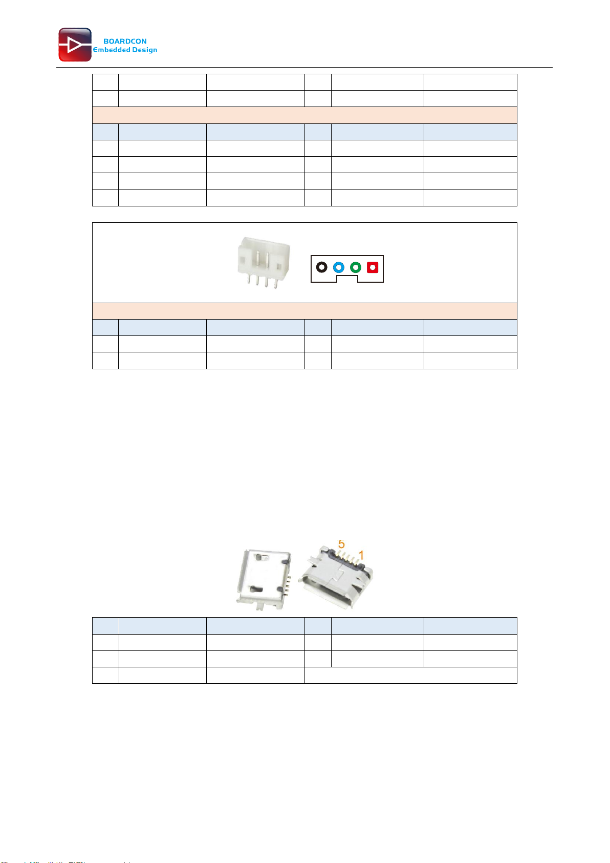
2.4 USB OTG
The USB2.0 OTG is used to upgrade Firmware or transmit files.
- Compatible with USB2.0 Specification
- Support High-Speed (HS,480 Mbit/s), Full-Speed (FS,12 Mbit/s), and Low-Speed (LS,1.5 Mbit/s)
in host mode
- Supports High-Speed (HS, 480 Mbit/s), Full-Speed (FS, 12 Mbit/s) in device mode
- Up to 8 user-configurable endpoints for Bulk, Isochronous, Control and Interrupt (Endpoint1,
Endpoint2, Endpoint3, Endpoint4)
Pin
Signal
Description
Pin
Signal
Description
1
USBVBUS
5V power supply
2
USB-DM0
USB D-
3
USB-DP0
USB D+
4
USB_ID
USB detect
5
GND
Ground
2.5 AV_IN
TV decoder supports 4-ch analog CVBS or 1-ch YPbPr(480i/576i/480p/576p) signal input.
2 1
3
4
1
5
Table of contents
Other Boardcon Motherboard manuals
