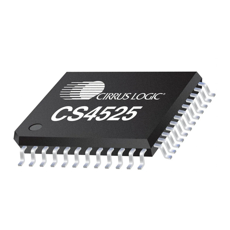
Cirrus Logic CS4525 Guide

http://www.cirrus.com
Copyright ©Cirrus Logic, Inc. 2007
(All Rights Reserved)
2 x 15 W CS4525 Digital Amplifier Reference Design
Features
Output Filters Optimized for 8 ΩLoads
Delivers 15 W/Ch into 8 Ωat 0.5 % THD+N
Single-Ended 2 VRMS Stereo Analog Inputs
Optical and Coaxial S/PDIF Inputs
Demonstrates EMI Compliant Design per FCC
Class B Part 15 and CISPR 22 Standards
Flexible I/O Headers Provided
– PCM Input Signal Interface
– Auxiliary Serial Port Signal Interface
– Delay Port Signal Interface
– PWM Logic Level Signal Interface
Optional CRD4412A Daughter-Card for
Subwoofer Channel
– Implements a 2.1 Configuration
Demonstrates Recommended 4-Layer Layout
and Grounding Arrangements
+18 V Switching Mode Power Supply Included
Can be operated by On-Board Controls or with
Windows®Compatible Graphical User
Interface
Description
The CRD4525-Q1 demonstrates the CS4525 digital
PWM controller with integrated power stages. This ref-
erence design implements a two-channel amplifier that
delivers 15 W per full-bridge channel into 8 Ωloads us-
ing a single +18 V supply. The CRD4525-Q1 is
powered by an included 80 W switching mode power
supply.
Standard RCA phono jacks are provided to easily inter-
face analog input signals with the evaluation board.
Optical and coaxial inputs are provided to interface with
S/PDIF digital audio input signals.
The PWM audio power outputs are routed through an
inductor/capacitor 2nd order low-pass filter (LPF) to re-
move high-frequency components from the output
signal, effectively converting it from digital to analog.
The Windows software provides a GUI to make config-
uration of the CRD4525-Q1 easy. The software
communicates through the PC’s USB port to configure
the control port registers so that all features of the
CS4525 can be evaluated. Additionally, control over ba-
sic functions is possible via on-board hardware controls
without the need to attach the CRD4525-Q1 to a PC.
ORDERING INFORMATION
CRD4525-Q1 CS4525 Reference Design
CS4525
Stereo Analog
Inputs
Optical
Receiver
Output
Filter
Speaker
Connector
Coaxial Input
CS8416
S/PIDF
Receiver
PCM
Input
Header
USB
I/O Micro-controller
Status LED’s
Tactile Controls
Aux Port Header
CRD4412A Interface Header
Power
Jack
Included 18 V Power Supply
8
8
Output
Filter
Ω
Ω
CRD4525-Q1
OCTOBER '07
DS804RD4

2DS804RD4
CRD4525-Q1
TABLE OF CONTENTS
1. SYSTEM OVERVIEW ............................................................................................................................. 4
1.1 Power ............................................................................................................................................... 4
1.2 CS4525 Digital Amplifier .................................................................................................................. 4
1.3 CS8416 Digital Audio Receiver ........................................................................................................ 4
1.4 System Clocking .............................................................................................................................. 4
1.5 External Data Headers ..................................................................................................................... 4
1.6 Analog Inputs ................................................................................................................................... 5
1.7 Speaker Outputs .............................................................................................................................. 5
1.8 PC Control ....................................................................................................................................... 5
1.9 Stand-Alone Control ......................................................................................................................... 5
1.10 External Power Stage Interface ..................................................................................................... 6
2. PC SOFTWARE CONTROL ................................................................................................................... 7
2.1 CS4525 Main Controls Tab .............................................................................................................. 7
2.2 CS4525 Aux & Filter Controls Tab ................................................................................................... 8
2.3 S/PDIF Input Controls Tab ............................................................................................................... 9
2.4 Register Maps Tab ......................................................................................................................... 10
2.5 Pre-Configured Script Files ............................................................................................................ 11
2.5.1 Analog In ............................................................................................................................... 11
2.5.2 Optical SPDIF In .................................................................................................................... 11
2.5.3 Coaxial SPDIF In ................................................................................................................... 11
3. STAND-ALONE MODE CONTROL ..................................................................................................... 12
4. GROUNDING AND POWER SUPPLY DECOUPLING ........................................................................ 12
4.1 Power Supply Decoupling .............................................................................................................. 12
4.2 Electromagnetic Interference (EMI) ............................................................................................... 12
4.2.1 Suppression of EMI at the Source .........................................................................................13
5. SYSTEM CONNECTIONS & JUMPERS .............................................................................................. 14
6. CRD SCHEMATICS .............................................................................................................................. 15
7. CRD LAYOUT ...................................................................................................................................... 18
8. PERFORMANCE PLOTS ..................................................................................................................... 23
9. THERMAL DE-RATING ........................................................................................................................ 29
10. ELECTROMAGNETIC COMPLIANCE (EMC) PERFORMANCE ...................................................... 30
10.1 EMI Testing Procedures .............................................................................................................. 30
10.2 System Configuration ................................................................................................................... 31
10.3 CRD4525-Q1 Test Results .......................................................................................................... 31
11. REVISION HISTORY .......................................................................................................................... 32
LIST OF FIGURES
Figure 1.Speaker Terminal Configuration ................................................................................................... 5
Figure 2.CS4525 Main Controls Tab ........................................................................................................... 7
Figure 3.CS4525 Aux & Filter Controls Tab ................................................................................................ 8
Figure 4.S/PDIF Input Controls Tab ............................................................................................................ 9
Figure 5.Register Maps Tab ...................................................................................................................... 10
Figure 6.CS4525 - Schematic Page 1 ....................................................................................................... 15
Figure 7.USB Microcontroller & Tactile Control - Schematic Page 2 ........................................................ 16
Figure 8.Power & I/O Connections - Schematic Page 3 ........................................................................... 17
Figure 9.Component Map ......................................................................................................................... 18
Figure 10.Top-Side Copper Layer ............................................................................................................. 19
Figure 11.Inner Copper Layer 1 ................................................................................................................ 20
Figure 12.Inner Copper Layer 2 ................................................................................................................ 21
Figure 13.Bottom-Side Copper Layer ....................................................................................................... 22
Figure 14.Frequency Response ................................................................................................................ 23
Figure 15.THD+N vs. Power ..................................................................................................................... 24

DS804RD4 3
CRD4525-Q1
Figure 16.THD+N vs. Frequency .............................................................................................................. 25
Figure 17.FFT at -60 dB Input ................................................................................................................... 26
Figure 18.FFT at 0 dB Input ...................................................................................................................... 27
Figure 19.Inter-Modulation Distortion of 19 kHz + 20 kHz ........................................................................ 28
Figure 20.Thermal De-Rating Curve for a Typical CRD4525-Q1 .............................................................. 29
Figure 21.Test Facility Setup .................................................................................................................... 30
Figure 22.Vertical Peak Scan Data for the CRD4525-Q1 ......................................................................... 31
Figure 23.Horizontal Peak Scan Data for the CRD4525-Q1 ..................................................................... 31
LIST OF TABLES
Table 1. System Connections ................................................................................................................... 14
Table 2. On-Board Tactile Controls ........................................................................................................... 14
Table 3. System Headers .......................................................................................................................... 14

4DS804RD4
CRD4525-Q1
1. SYSTEM OVERVIEW
The CRD4525-Q1 reference design is an excellent means for evaluating the CS4525 30 W digital amplifier with in-
tegrated ADC. Analog and digital audio input signal interfaces are provided; an on-board microcontroller and USB
PC interface is used for easily configuring the CS4525’s internal registers, and stand-alone mode is supported
through on-board tactile controls.
The CRD4525-Q1 schematic set is shown in Figure 6 through Figure 8.
1.1 Power
A 80 W OEM switching-mode power supply is included to power the CRD4525-Q1. The power supply pro-
vides +18 V to the CS4525 power stages, and an on-board buck-converter and regulator provide power to
the logic-level digital circuitry.
Power may be supplied from the included power supply or any 12-18 VDC power supply capable of deliv-
ering sufficient current for the intended power output. Connection for the power supply is provided in J3 (see
the System Connections table on page 14).
1.2 CS4525 Digital Amplifier
A complete description of the CS4525 is included in the CS4525 product data sheet.
Optional user configuration settings of the CS4525 are provided through its control port registers, accessible
through the CS4525 tab of the Cirrus Logic FlexGUI software. A register-level configuration interface is pro-
vided on the Register Maps tab. See the “PC Software Control” section on page 7 for more information.
1.3 CS8416 Digital Audio Receiver
A complete description of the CS8416 receiver (Figure 8 on page 17) and a discussion of the digital audio
interface are included in the CS8416 data sheet.
The CS8416 converts the input S/PDIF data stream into PCM data and clocks for the CS4525. The CS8416
operates in master mode and can provide PCM data in Left-Justified, I²S, Right-Justified 16-bit, and Right-
Justified 24-bit interface formats.
The most common operations of the CS8416 may be controlled via the S/PDIF Input Controls tab in the GUI
software application. Advanced options are accessible through the CS8416 sub-tab on the Register Maps
tab of the Cirrus Logic FlexGUI software.
1.4 System Clocking
A 24.576 MHz parallel resonant crystal, Y1, is available to provide a clock source to the CS4525. The crystal
is mounted in pin sockets, allowing easy removal or replacement. Alternatively, an input SYS_CLK signal
can be provided on pin 3 of the serial audio input header (J2).
1.5 External Data Headers
The evaluation board has been designed to allow interfacing with external systems via the headers J2, J4,
and J11. Figure 6 shows the headers’ electrical connections.
The 12-pin, 3 column header, J2, provides access to the CS4525’s serial audio input and SYS_CLK input
signals. Place shunts across the SCLK, LRCK, and SDIN pins located in the columns labeled “S/PDIF” to
connect to the on-board S/PDIF digital interface receiver circuitry. To use an external digital audio source,
simply remove the shunts and connect a ribbon across the SCLK, LRCK, and SDIN pins located in the col-

DS804RD4 5
CRD4525-Q1
umns labeled “EXT SAI”. A single ground column for the ribbon cable’s ground connection is provided to
maintain signal integrity.
The 8-pin, 2 column header, J11, provides access to the CS4525’s auxiliary serial audio port output signals,
as well as the SYS_CLK output signal. A single ground column is provided to maintain signal integrity.
The 20-pin, 2 column header, J4, is included to interface with a CRD4412A card. Various signals, power,
and ground are presented on this header. Notably, this header includes the DLY_SDOUT and DLY_SDIN
signals which can be used to interface with an external delay device or DSP. See Figure 6 for complete con-
nectivity information.
1.6 Analog Inputs
RCA connectors supply the CS4525 analog inputs through single-ended passive circuits with one pole of
input filtering. A resistive attenuation network is implemented to allow 2 VRMS input levels to be supplied to
the CRD4525-Q1. Refer to the CS4525 data sheet for the maximum input signal level at the analog input
pins.
1.7 Speaker Outputs
The CS4525 power outputs are configured for stereo full-bridge operation. The outputs are routed through
a 2nd order low-pass filter to remove high-frequency content from the output signals and then presented at
the speaker wire crimp terminals (J5). The output filters are optimized for 8 Ωspeaker loads. The speaker
terminal connections are shown below.
1.8 PC Control
A USB connection is provided to facilitate software control of the CS4525’s internal registers.
A graphical user interface is available for the CRD4525-Q1 to allow easy manipulation of the CS4525’s in-
ternal registers. See the CS4525 data sheet for complete internal register descriptions.
To enable the CRD4525-Q1, simply connect the supplied USB cable from an available USB port on a PC
to the USB connector (J37) and launch the Cirrus Logic FlexGUI software.
A visual indicator is provided by an on-board LED (D12) that illuminates when the board is being operated
under PC control. When operating under PC Control, the stand-alone controls on the board should not be
manipulated.
Refer to “PC Software Control” on page 7 for a description of the Graphical User Interface (GUI).
1.9 Stand-Alone Control
A volume control knob (S1), reset button (S2), and mute button (S3) are included for stand-alone operation
of the CRD4525-Q1. These controls were not supported by early versions of firmware running on the
CRD4525-Q1, so it may be necessary to upgrade older firmware versions to enable their functionality.
RL
Figure 1. Speaker Terminal Configuration

6DS804RD4
CRD4525-Q1
The on-board firmware can be upgraded by downloading and running the most recent version of the Cirrus
Logic FlexGUI application. If necessary, this application (downloadable at www.cirrus.com/msasoftware)
will automatically upgrade the firmware for an attached CRD4525-Q1 upon start-up.
1.10 External Power Stage Interface
A keyed connector (J4) is included to interface with the CRD4412A. The CRD4525-Q1 can be used with or
without a CRD4412A attached.
Without the CRD4412A attached, the CRD4525-Q1 configures itself for 2-channel stereo full-bridge opera-
tion. When the CRD4412A is attached, the CS4525 enables its bass manager and routes the LFE channel
to the CRD4412A which amplifies the signal in mono parallel full-bridge mode. Together, the CRD4525-Q1
and CRD4412A implement a 2.1 configuration.
The CRD4412A must be inserted and removed while power is not applied to the CRD4525-Q1.

DS804RD4 7
CRD4525-Q1
2. PC SOFTWARE CONTROL
The CRD4525-Q1 is designed for use with the Microsoft®Windows-based FlexGUI graphical user interface. This
interface provides comprehensive control over the CS4525’s internal registers via a PC’s USB port.
The FlexGUI software may be downloaded and installed from www.cirrus.com/msasoftware.
Step-by-step instructions for using the FlexGUI are provided as follows:
1. Download and install the FlexGUI software from www.cirrus.com/msasoftware.
2. Connect the CRD4525-Q1 to a host PC using the supplied USB cable.
3. Connect load speakers to the speaker output terminals.
4. Connect an input source to the S/PDIF or analog input connectors.
5. Plug the input to the included +18 V power supply into an available power outlet.
6. Plug the output of the included +18 V power supply into the power input connector on the CRD4525-Q1.
7. Launch the FlexGUI software. The GUI will load and be displayed.
8. Un-check the “Power Down CS4525” checkbox to power-up the device. In this state, the CRD4525-Q1 will
convert and amplify the content present on the optical S/PDIF input.
2.1 CS4525 Main Controls Tab
The CS4525 Main Controls tab provides a high-level, intuitive interface to many of the basic configuration
options of the CS4525. Use this tab to access functions such as power-down, input source, and volume con-
trol.
Figure 2. CS4525 Main Controls Tab

8DS804RD4
CRD4525-Q1
2.2 CS4525 Aux & Filter Controls Tab
The CS4525 Aux & Filter Controls tab provides a high-level, intuitive interface to many of the advanced con-
figuration options of the CS4525. Use this tab to configure the auxiliary port, the internal filters, and ad-
vanced PWM adjustments. Control over device and board resets is also provided.
The CS4525 Parametric EQ Filter Wizard, available for download from the CS4525 product page at
www.cirrus.com, provides a graphical interface to the Parametric Equalization, Bass Manager, and Tone
Control features of the CS4525. Using this utility, the user can graphically configure any or all of the five on-
chip bi-quad filters, the Bass Manager crossover frequency, and the bass/treble shelving filters available in
the CS4525.
This utility creates a script file which can be loaded into the CS4525 utilizing the FlexGUI interface. Please
refer to Cirrus Logic application note AN303 for more information regarding this valuable tool.
Figure 3. CS4525 Aux & Filter Controls Tab

DS804RD4 9
CRD4525-Q1
2.3 S/PDIF Input Controls Tab
When the CRD4525-Q1 is configured to make use of the CS8416 S/PDIF receiver, the devices must be
configured for proper operation. The S/PDIF Input Controls tab provides a high-level, intuitive interface to
the most common configuration options of the CS8416.
Figure 4. S/PDIF Input Controls Tab

10 DS804RD4
CRD4525-Q1
2.4 Register Maps Tab
The Register Maps tab provides an easy register-level interface to the on-board devices. Register values
can be modified on a bit-wise or byte-wise basis. To modify a single bit, first select the register by clicking
its position in the register matrix; then click the appropriate push-button for the desired bit. To modify an
entire register, simply enter the register’s new value directly into the register matrix.
Within the Register Maps tab, the CS4525 tab is used to access the CS4525’s internal registers, and the
CS8416 tab is used to access the CS8416’s internal registers.
Figure 5. Register Maps Tab

DS804RD4 11
CRD4525-Q1
2.5 Pre-Configured Script Files
Pre-configured script files are provided with the CRD4525-Q1 to allow easy initial board bring-up. The board
configurations stored within these files are described in Sections 2.5.1 - 2.5.3.
2.5.1 Analog In
Using the pre-configured script file named “Analog In.fgs”, an analog input signal applied to the analog
inputs of the CRD4525-Q1 will be used as the CS4525’s input source. The device will be powered up with
no internal processing active and the master volume control set to -20 dB.
2.5.2 Optical SPDIF In
Using the pre-configured script file named “Optical SPDIF In.fgs”, the optical S/PDIF input signal will be
received by the CS8416 S/PDIF receiver. The CS8416 PCM output signals will be used as the CS4525’s
input source. The device will be powered up with no internal processing active and the master volume
control set to -20 dB.
2.5.3 Coaxial SPDIF In
Using the pre-configured script file named “Coaxial SPDIF In.fgs”, the coaxial S/PDIF input signal will be
received by the CS8416 S/PDIF receiver. The CS8416 PCM output signals will be used as the CS4525’s
input source. The device will be powered up with no internal processing active and the master volume
control set to -20 dB.

12 DS804RD4
CRD4525-Q1
3. STAND-ALONE MODE CONTROL
The CRD4525-Q1 is capable of operation without being connected to a computer by operating in stand-alone mode.
When in this mode, the board is controlled by on-board hardware controls detailed in Table 2 on page 14.The rotary
volume control on the edge of the board controls the volume. Tapping the mute button mutes/un-mutes the PWM
outputs of the CS4525.
When a valid SPDIF signal is not present, the CS4525 is automatically configured to amplify the audio signal present
on the RCA analog input connectors. When a valid SPDIF signal is present, the CS4525 is automatically configured
to amplify the audio signal present in the SPDIF stream. Holding down the mute button for three seconds switches
between optical SPDIF input and coaxial SPDIF input.
4. GROUNDING AND POWER SUPPLY DECOUPLING
The CS4525 requires careful attention to power supply and grounding arrangements to optimize performance and
heat dissipation and minimize radiated emissions. Figure 9 on page 18 shows the component placement. Figure 11
on page 20 shows the top layout. Figure 13 on page 22 shows the bottom layout. The decoupling capacitors are
located as close to the CS4525 as possible. Extensive use of ground plane fill in the evaluation board yields large
reductions in radiated noise.
4.1 Power Supply Decoupling
Proper power supply decoupling is one key to maximizing the performance of a Class-D amplifier. Because
the design uses an open loop output stage, noise on the power supply rail will be coupled to the output.
Careful decoupling of the power stage supply rails is essential. Figure 9 on page 18 demonstrates good de-
coupling capacitor placement. Notice that the small value decoupling capacitors are placed as close as
physically possible to the power pins of the CS4525. The ground side of the capacitors is connected directly
to top side ground plane, which is also used by the power supply return pins. This keeps the high frequency
current loop small to minimize power supply variations and EMI. 470 µF electrolytic capacitors are also lo-
cated in close proximity to the power supply pins to supply the current locally for each channel. These are
not required to be expensive low-ESR capacitors. General-purpose electrolytic capacitors that are specified
to handle the ripple current can be used.
4.2 Electromagnetic Interference (EMI)
The EMI challenges that face a maker of Class-D amplifiers are largely the same challenges that have been
faced by the switch mode power supply industry for many years. The numerous EMI consulting firms that
have arisen and the many books that have been written on the subject indicate the scope of potential prob-
lems and available solutions. They should be considered a resource - most makers of switch mode equip-
ment would benefit from developing a working relationship with a qualified EMI lab and from bringing their
experience to bear on design issues, preferably early in the design process.
This reference design is a board-level solution which is meant to control emissions by minimizing and sup-
pressing them at the source, in contrast to containing them in an enclosure.
The EMI requirements for an amplifier have added dimensions beyond those imposed on power supplies.
Audio amplifiers are usually located in close proximity to radio receivers, particularly AM receivers which are
notoriously sensitive to interference. Amplifiers also need to operate with speaker leads of unpredictable
length and construction which makes it possible for any high-frequency currents that appear on the outputs
to generate nuisance emissions.
For more detailed information regarding the EMI performance of the CRD4525-Q1, please refer to Section
10. “Electromagnetic Compliance” on page 30.

DS804RD4 13
CRD4525-Q1
4.2.1 Suppression of EMI at the Source
Several techniques are used in the circuit design and board layout to minimize high frequency fields in the
immediate vicinity of the high power components. Specific techniques include the following:
• As mentioned in Section 4.1, effective power supply decoupling of high-frequency currents and mini-
mizing the loop area of the decoupling loop is one aspect of minimizing EMI.
• Each output of the CS4525 includes “snubbing” components. For example, OUT1 includes snubber
components R24 (5.62 Ω) and C23 (680 pF). These components serve to damp ringing on the switch-
ing outputs in the 30-50 MHz range. The snubbing components should be as close as practical to the
output pins to maximize their effectiveness.
• A separate ground plane with a solid electrical connection to the chassis, and which surrounds the
speaker output connector, should be implemented. This allows the speaker outputs to be RF decou-
pled to the chassis just before they exit the chassis from the speaker connector.
• Make use of source termination resistors on all digital signals whose traces are longer than about
25 mm.

14 DS804RD4
CRD4525-Q1
5. SYSTEM CONNECTIONS & JUMPERS
Connector
Name
Reference
Designator
Signal
Direction Connector Function
Power In J3 Input Power Connector. 12 to 18 VDC
Left In
Right In
J1
J10 Input Analog input to CS4525
S/PIDF Input J6 Input Coaxial digital input to CS8416
S/PIDF Input J7 Input Optical digital input to CS8416
Speaker
Connector J5 Output Analog output from CS4525
USB J8 Input/Output USB connection to PC for software control
C2 J9 Input/Output Connection for programming the on-board microcontroller (U3)
Table 1. System Connections
Control Name
Reference
Designator Tactile Control Function
Master Volume S1 Controls settings of the volume control register
Board Reset S2 Resets all devices in system
Mute S3 Sets outputs of CS4525 to 50/50 duty cycle mute
Table 2. On-Board Tactile Controls
Connector Name
Reference
Designator Header Function
DSP IN J2
When shunts are placed across column 1 and 2, the CS4525 serial audio
input data is sourced by the CS8416
To use external serial audio input data, connect the PCM source cable
across column 2 and 3
DSP OUT J11 Auxiliary serial audio data from the CS4525
CRD4412 I/F J4 Connection to CRD4412A daughter card
Table 3. System Headers
Other manuals for CS4525
1
Table of contents
Other Cirrus Logic Amplifier manuals


