Cronologic Ndigo5G-8 User manual
Revision 1.0.8 as of 2018-11-19
Firmware 2 (build 4865), Driver v1.3.0
cronologic GmbH & Co. KG
Ndigo5G-8
Ndigo5G-10
User Guide
cronologic


Contents
1 Introduction 1
1.1 Features ......................................... 1
2 Hardware 3
2.1 Installing the Board .................................. 3
2.2 Ndigo5G External Inputs and Connectors ...................... 4
2.2.1 Connectors ................................... 4
2.2.2 Analog Inputs ................................. 5
2.2.3 Digital Inputs .................................. 6
2.3 Extension Card ..................................... 7
2.4 Ndigo5G Functionality ................................. 8
2.4.1 ADC Modes ................................... 8
2.4.2 Zero Suppression ................................ 10
2.4.3 Trigger Blocks ................................. 10
2.4.4 Gating Blocks .................................. 15
2.4.5 Auto Triggering Function Generator ..................... 18
2.4.6 Timestamp Channel .............................. 18
2.4.7 Data Lookup Table ............................... 19
2.5 Multiple Ndigo boards synchronization ........................ 19
2.5.1 Calibration Procedure ............................. 20
2.5.2 Synchronizing a Ndgio5G and an HPTDC8-PCI .............. 22
2.6 Performing a firmware update ............................. 22
2.7 Calibrating the TDC .................................. 23
3 Driver Programming API 25
3.1 Constants ........................................ 25
3.2 Initialization ...................................... 25
3.2.1 Structure ndigo init parameters ........................ 25
3.3 Status Information ................................... 27
3.3.1 Functions for Information Retrieval ...................... 27
3.3.2 Structure ndigo static info ........................... 27
3.3.3 Structure ndigo param info .......................... 29
3.3.4 Structure ndigo fast info ............................ 29
3.3.5 Structure ndigo slow info ........................... 30
3.4 Configuration ...................................... 30
3.4.1 Structure ndigo configuration ......................... 31
3.4.2 Structure ndigo trigger ............................. 33
3.4.3 Structure ndigo trigger block ......................... 34
3.4.4 Structure ndigo gating block ......................... 36
3.4.5 Structure ndigo extension block ........................ 37
3.4.6 Run Time Control ............................... 37
3.5 Readout ......................................... 38
3.5.1 Input Structure ndigo read in ......................... 38
3.5.2 Input Structure ndigo read out ........................ 38
i

Contents
3.6 Other Functions .................................... 38
3.6.1 LED control ................................... 38
4 Packet Format 41
4.0.1 Output Structure ndigo packet ........................ 41
5 C Example 43
6 Technical Data 45
6.1 Digitizer Characteristics ................................ 45
6.1.1 1-Channel-Mode (5Gsps) ........................... 45
6.1.2 2-Channel-Mode (2.5 Gsps) .......................... 45
6.1.3 4-Channel-Mode (1.25 Gsps) ......................... 46
6.2 Electrical Characteristics ............................... 46
6.2.1 Oscillator .................................... 46
6.2.2 Environmental Conditions for Operation ................... 46
6.2.3 Environmental Conditions for Storage .................... 46
6.2.4 Power Supply .................................. 47
6.2.5 Analog Input .................................. 47
6.3 Information Required by DIN EN 61010-1 ...................... 47
6.3.1 Manufacturer .................................. 47
6.3.2 Intended Use and System Integration .................... 48
6.3.3 Cooling ..................................... 48
6.3.4 Environmental Conditions ........................... 48
6.3.5 Inputs ...................................... 48
6.3.6 Recycling .................................... 48
ii

1 Introduction
The Ndigo5G is a digitizer and transient recorder designed to sample relatively shorts pulses
in rapid repetition. It produces a stream of output packets, each containing data from a single
trigger event together with a timestamp.
1.1 Features
10 bit dynamic range
up to 5 Gsps sample rate (in 1 channel mode)
up to 4 channels
digital input with TDC that can also be used for gating and triggering
2nd digital input for gating or triggering
PCIe 4x 1.1 with 800 MB/s throughput
multiple boards can be synchronized
extension board with 4 additional digital inputs.
1


2 Hardware
2.1 Installing the Board
The Ndigo5G board can be installed in any x4 (or higher amount of lanes) PCIe slot. If the slot
electrically supports less than 4 lanes, the board will operate at lowerdata throughput rates.
Please ensure proper cooling of the device. The Ndigo5G has an onboard temperature detec-
tion. If the ADC chip temperature exceeds 90◦C a warning is issued to the device driver. In case
the temperature is higher than 95◦C the ADC is disabled to avoid damage. Using a PCI-slot
cooler is in many cases an appropriate solution to circumvent problems caused by overheating
if the board is used inside a PC. The Ndigo-Crate will provide sufficient cooling under normal
operating conditions.
Using a single Ndigo5G, no further connections need to be made. For applications that
require more than 4 ADC channels, several Ndigo boards can be operated in sync. Any board
of the Ndigo product line can be synced to other Ndigo boards, allowing, for instance, for a
combination of high speed ADCs (Ndigo5G) and slower high resolution ADCs (Ndigo250M-14)
or the upcoming Ndigo TDC.
The signals used for board synchronization and inter-board triggering are transferred on a
bus be-tween the boards. Join all C2 connectors (see Figure 2.3 on page 5) on the boards using
a ribbon cable. Both ends of the bus need to be terminated properly. If using a Ndigo Crate,
connectors providing the termination are located on the crate mainboard next to the PCIe slots
to the extreme left and right. For more details, please refer to the Ndigo Crate user guide. In
applications that use only a few Ndigo boards installed directly inside a PC, termination PCBs
available from cronologic can be used.
Ndigo5G’s standard device driver can be used to read out all boards and acquire data. For
more complex scenarios, using the cronoSync-library, which is part of cronoTools, is recom-
mended. The cronoSync library is provided with the Ndigo device driver. Please refer to the
cronoTools user guide for more information.
3

C1
C1
C1
termination
termination
C2
C2
C2
Figure 2.1: If several Ndigo boards are connected to work in sync , the boards must be connected
using a ribbon cable as bus for synchronization and trigger signals. At both ends of
the cable, proper termination is required.
2.2 Ndigo5G External Inputs and Connectors
2.2.1 Connectors
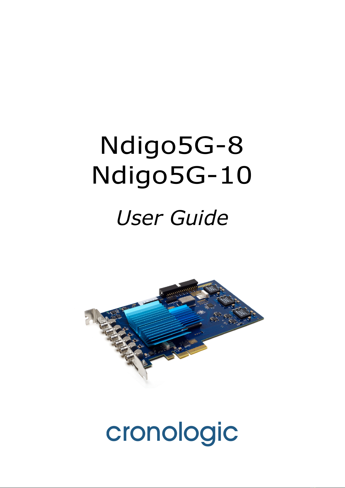
The inputs of the Ndigo5G are located on the PCI bracket. Figure 2.3 on page 5shows the
location of the 4 analog inputs A to D and the two digital inputs G (GATE) and T (Trigger).
Furthermore, two board interconnection connectors can be found at the top edge of the Ndigo5G,
as displayed in Figure 2.3 on page 5. Connector C1 is used for a board-to-board connection (e. g.
to link a HPTDC8-PCI and a Ndigo5G via a Ndigo Extension board, see chapter 2.3). Connector
C2 is used as a bus interface between multiple Ndigo boards distributing clock, trigger and sync
signals. Proper termination must be placed at both ends of the bus interconnection ribbon
cable.
Figure 2.2: Input connectors of an Ndigo5G located on the PCI bracket.
cronologic GmbH & Co. KG 4 Ndigo5G User Guide
B
C2
C
D
T
G
C1
A
Figure 2.3: Schematics of an Ndigo5G board showing inter-board connectors C1 and C2.
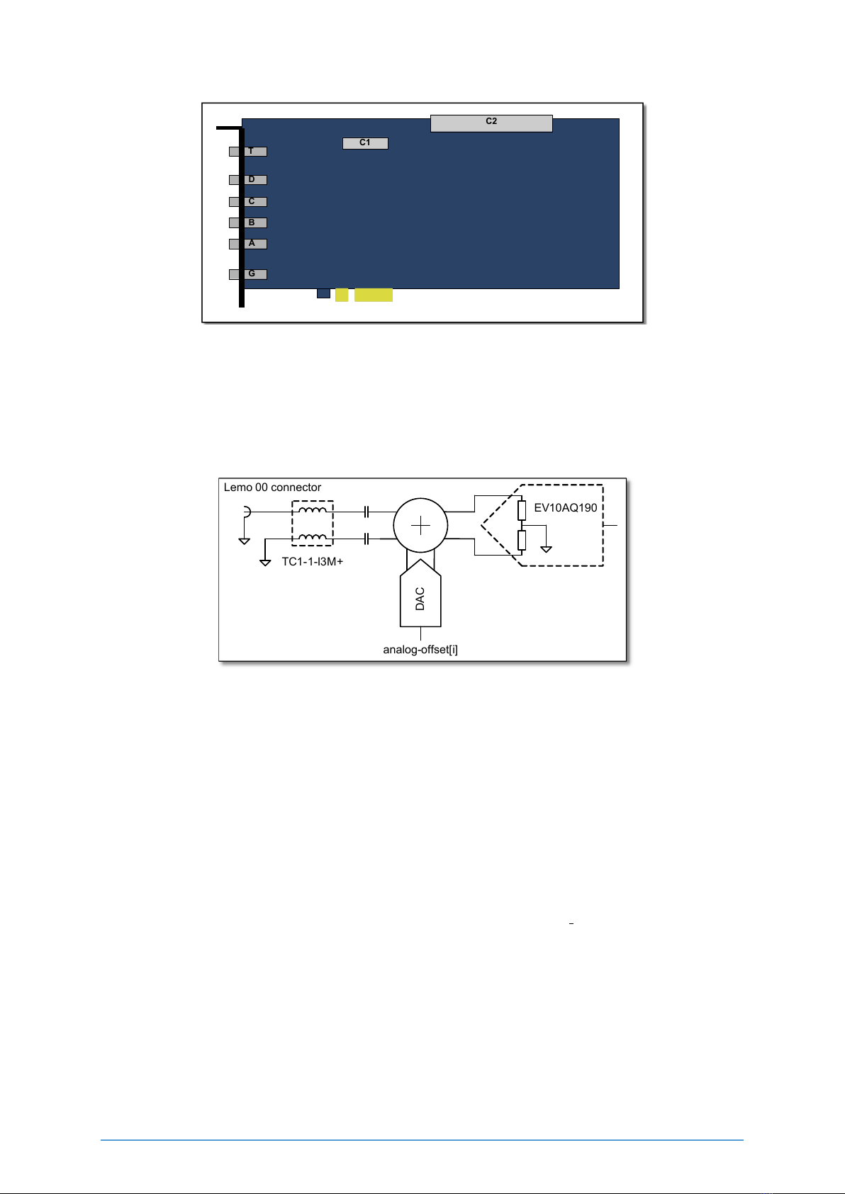
2.2.2 Analog Inputs
TC1-1-I3M+
Lemo 00 connector
analog-offset[i]
EV10AQ190
DAC
Figure 2.4: Input circuit for each of the four analog channels.
The analog inputs of the ADC are single ended LEMO00 coax connectors. The inputs have
a 50Ω impedance and are AC coupled. The inputs are converted to a differential signal using a
balun.
Analog Offsets
AC coupling removes the common mode voltage from the input signal. Users can move the
common mode voltage to a value of their choice using the analog offset parameter of each
channel before sampling.
This feature is useful for highly asymmetric signals, such as pulses from TOF spectrometers
or LIDAR systems. Without analog offset compensation, the pulses would begin in the middle
of the ADC range, effectively cutting the dynamic range in half (see Figure 2.6). By shifting
the DC baseline to one end of the ADC range, the input range can be used fully, providing the
maximum dynamic range. The analog offset can be set between ±0,25V.
cronologic GmbH & Co. KG 5 Ndigo5G User Guide

+0,25V
analog_offset[i] = 0V
-0,25V
+0,25V
analog_offset[i] = 0,1V
-0,25V
0,1V
Figure 2.5: Users can add analog offset to the input before sampling
+0,25V
analog_offset[i] = 0V
-0,25V
+0,25V
analog_offset[i] = 0,22V
-0,25V
0,22V
Figure 2.6: Asymmetric signal shifted to increase dynamic range
2.2.3 Digital Inputs
There are two digital inputs on the front slot cover called Trigger and GATE.
Both inputs provide a digital input signal routed to the trigger matrix. These signals can be
used to trigger any of the trigger state machines and gating blocks. The inputs are AC coupled.
DC offset is configurable via the dc offset parameter in the configurations structure to support
positive and negative input pulses.
The configuration is set via the structures trigger[8] and trigger[9] in the configuration struc-
ture. The input circuit is shown in Figure 2.17 on page 13.
TDC on Trigger Input
There is a TDC connected to the Trigger input. When used with the TDC, the Trigger input
supports negative pulses only . The TDC creates packets of type 8. These packets first contain
a coarse timestamp and a payload that can be used to calculate the trigger position with higher
precision. The function ndigo process tdc packet() can be used to replace the coarse timestamp
with the precise timestamp. This function is described in section 3.5 on page 38. TDC pulses
must have a minimum duration of 3.3ns. The dead-time of the TDC is 32ns.
cronologic GmbH & Co. KG 6 Ndigo5G User Guide

2.3 Extension Card
The Ndigo Extension card provides additional inputs or outputs to the FPGA. It is connected
to the Samtec QSS-025 connector on an Ndigo5G by an Samtec SQCD cable assembly.
The Ndigo Extension Card provides up to ten single ended LEMO00 connectors. The circuit
connecting to each of these circuits can be chosen to provide inputs or outputs. These can be
AC or DC coupled. AC coupled inputs support NIM signaling.
The signals connect to 2.5V IO Pins of the Xilinx Virtex-5 FPGA. The current firmware
revision provides the following signal connections:
Connector QSS Pin FPGA Pin Direction Signal
LEMO00: CH0 22 AD9 Input Ndigo Extension digital channel 0
LEMO00: CH1 18 AE10 Input Ndigo Extension digital channel 1
LEMO00: CH2 14 D10 - not connected
LEMO00: CH3 10 AF9 Output 39 MHz clock for HPTDC
LEMO00: CH4 6 AD11 Output 39 MHz clock for HPTDC
LEMO00: CH5 5 AE7 Output 39 MHz clock for HPTDC
LEMO00: CH6 9 AF7 Output 39 MHz clock for HPTDC
LEMO00: CH7 13 D9 - not connected
LEMO00: CH8 17 V9 Input Ndigo Extension digital channel 2
LEMO00: CH9 21 W9 Input Ndigo Extension digital channel 3
SYNC1: Sync-TDC8 26 F9 - not connected
SYNC1: Sync-HPTDC 44 AA7 Output Sync for HPTDC
The 4 digital inputs are routed to the bus inputs of the trigger matrix to be used for triggering.
The routing can be configured to either ORing the sync bus and extension channels or use the
extension channels exclusively.
Connector Extension Card Trigger matrix input Trigger matrix input
Digital Channel ignore cable = 0 ignore cable = 1
LEMO00: CH0 0 BUS0 = EXT0 |Sync Cable 0 BUS0 = EXT0
LEMO00: CH1 1 BUS1 = EXT1 |Sync Cable 1 BUS1 = EXT1
LEMO00: CH8 2 BUS2 = EXT2 |Sync Cable 2 BUS2 = EXT2
LEMO00: CH9 3 BUS3 = EXT3 |Sync Cable 3 BUS3 = EXT3
cronologic GmbH & Co. KG 7 Ndigo5G User Guide

2.4 Ndigo5G Functionality
2.4.1 ADC Modes
Depending on board configuration, the analog input signal is quantized to 8 or 10 bits. However,
the board always scales and offsets the data to 16 bit signed data centered around 0.
Data processing such as trigger detection or packet building are always performed on 3.2ns
intervals. Depending on the ADC mode, this interval may contain 4, 8 or 16 samples.
The board supports using one, two or four channels:
1 Channel Modes A, B, C and D
In these modes, only a single channel is used. The analog signal on that channel is digitized at
5Gsps. Packet size is always a multiple of 16 samples per 3.2ns. See Figure 2.9 on page 9and
Figure 2.15 on page 13.
2 Channel Modes AC, BC, AD and BD
In these modes, two channels are used simultaneously. The analog signals on these channels are
digitized at 2.5Gsps each. Packet size is always a multiple of 8 samples per 3.2ns. See Figure
2.8 on page 9and Figure 2.14 on page 12.
4 Channel Mode ABCD
In this mode, all four channels are digitized independently at 1.25Gsps each. The packet size is
always a multiple of 4 samples per 3.2ns. See Figure 2.7 on page 9and Figure 2.13 on page 12.
Multiple Sampling Modes AAAA, BBBB, CCCC and DDDD
In these modes, only one analog input channel is used, but the channel is sampled independently
and simultaneously by four ADCs at 1.25Gsps. The board creates four independent streams with
4 samples each per 3.2ns.
Using the same trigger setting on all ADCs, can be used to reduce noise by averaging the four
channels. To deal with complex triggering conditions, different trigger settings on each of the
ADCs can be used.
The Ndigo5G provides 4 ADCs sampling at 1.25Gsps each. Higher speed modes are imple-
mented by interleaving two or four of these ADCs.
During interleaving, the Ndigo5G firmware reorders and groups the data into a linear sample
stream. The process is fully transparent. For users, the only difference is that a 3.2ns cycle can
contain 4, 8 or 16 samples, depending on mode.
cronologic GmbH & Co. KG 8 Ndigo5G User Guide

CLK
(2.5 GHz)
Clock
circuit
1.25 GHz
ADC A
1.25 Gsps
ADC B
1.25 Gsps
ADC C
1.25 Gsps
ADC D
1.25 Gsps
AAI, AAIN BAI, BAIN CAI, CAIN DAI, DAIN
Figure 2.7: ADCs in 4 channel mode ABCD at 1.25Gsps.
CLK
(2.5 GHz)
Clock
circuit
Inverted
1.25 GHz
ADC A
1.25 Gsps
ADC B
1.25 Gsps
ADC C
1.25 Gsps
ADC D
1.25 Gsps
AAI, AAIN DAI, DAIN
In-phase
1.25 GHz
Figure 2.8: ADCs in 2 channel mode AD, interleaved for 2.5Gsps.
CLK
(2.5 GHz) Clock
circuit
Inverted
1.25 GHz
ADC A
1.25 Gsps
ADC B
1.25 Gsps
ADC C
1.25 Gsps
ADC D
1.25 Gsps
AAI, AAIN or BAI,BAIN or CAI , CAIN or DAI , DAIN
In-phase
1.25 GHz
900phase-shifted
1.25 GHz
2700phase -shifted
1.25 GHz
Figure 2.9: ADCs in 1 channel mode A, B, C or D interleaved for 5Gsps.
cronologic GmbH & Co. KG 9 Ndigo5G User Guide
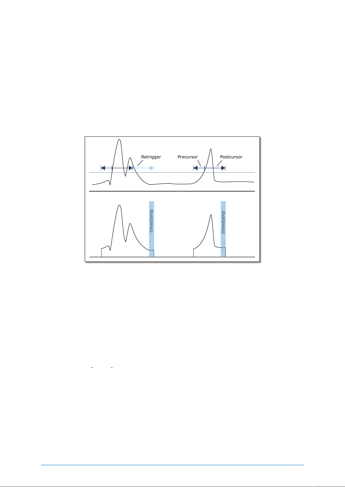
2.4.2 Zero Suppression
One of Ndigo5G’s key features is on-board zero suppression to reduce PCIe bus load. Only data
that passes specifications predefined by the user is transmitted. This guide refers to transmitted
waveform data as “packets”. A packet contains the waveform data and a timestamp giving the
absolute time (i.e. the time since start of data acquisition) of the packet’s last sample.
Figure 2.10 shows a simple example: Data is written to the PC only if values exceed a specified
threshold. Expanding on that, Ndigo5G’s zero suppression can be used to realize much more
complex scenarios.
timestamp
timestamp
Retrigger Precursor Postcursor
Figure 2.10: Simple zero suppression: Only data with values above a threshold are written to
the PC.
2.4.3 Trigger Blocks
Ndigo5G-10 and Ndigo5G-8 record analog waveforms using zero suppression. Whenever a rel-
evant waveform is detected, data is written to an internal FIFO memory. Each ADC channel
has one trigger block determining whether data is written to the FIFO. The parameters are set
in Structure ndigo trigger block(See chapter 3.4.3 on page 34).
Each trigger block consists of two independent units that check the incoming raw data stream
for trigger conditions (Fig. 2.10 on page 10). Users can specify a threshold and can choose
whether triggering is used whenever incoming data is below or above the threshold (level trig-
gering) or only if data exceeds the threshold (edge triggering).
A gate length can be set to extend the trigger window by multiples of 3.2ns. Furthermore, if
users choose precursor values >0, the trigger unit will start writing data to the FIFO precursor·
3.2ns before the trigger event.
When using edge triggering, all packets have the same length (Figure 2.11 on page 11):
cronologic GmbH & Co. KG 10 Ndigo5G User Guide
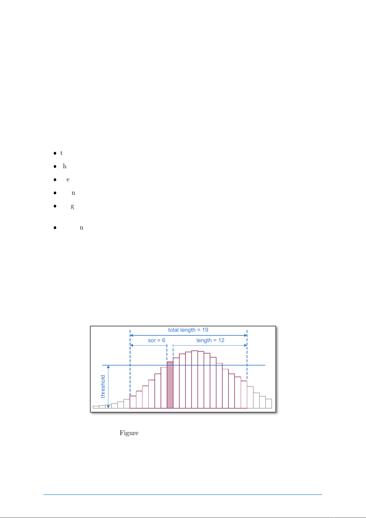
precursor + length + 1 cycles of 3.2ns. For level triggering, packet length is data dependent
(Figure 2.12 on page 12).
Please note that triggering is not accurate to sample. For each 3.2ns clock cycle, it is deter-
mined whether on any sample during that clock cycle a trigger condition is met. The clock cycle
is then selected as the trigger point. As a result, the trigger sample can be anywhere within a
range of up to 16 samples in single channel mode (Figure 2.15 on page 13) at 16 samples per
3.2ns.
If retriggering is active, the current trigger window is extended if a trigger event is detected
inside the window.
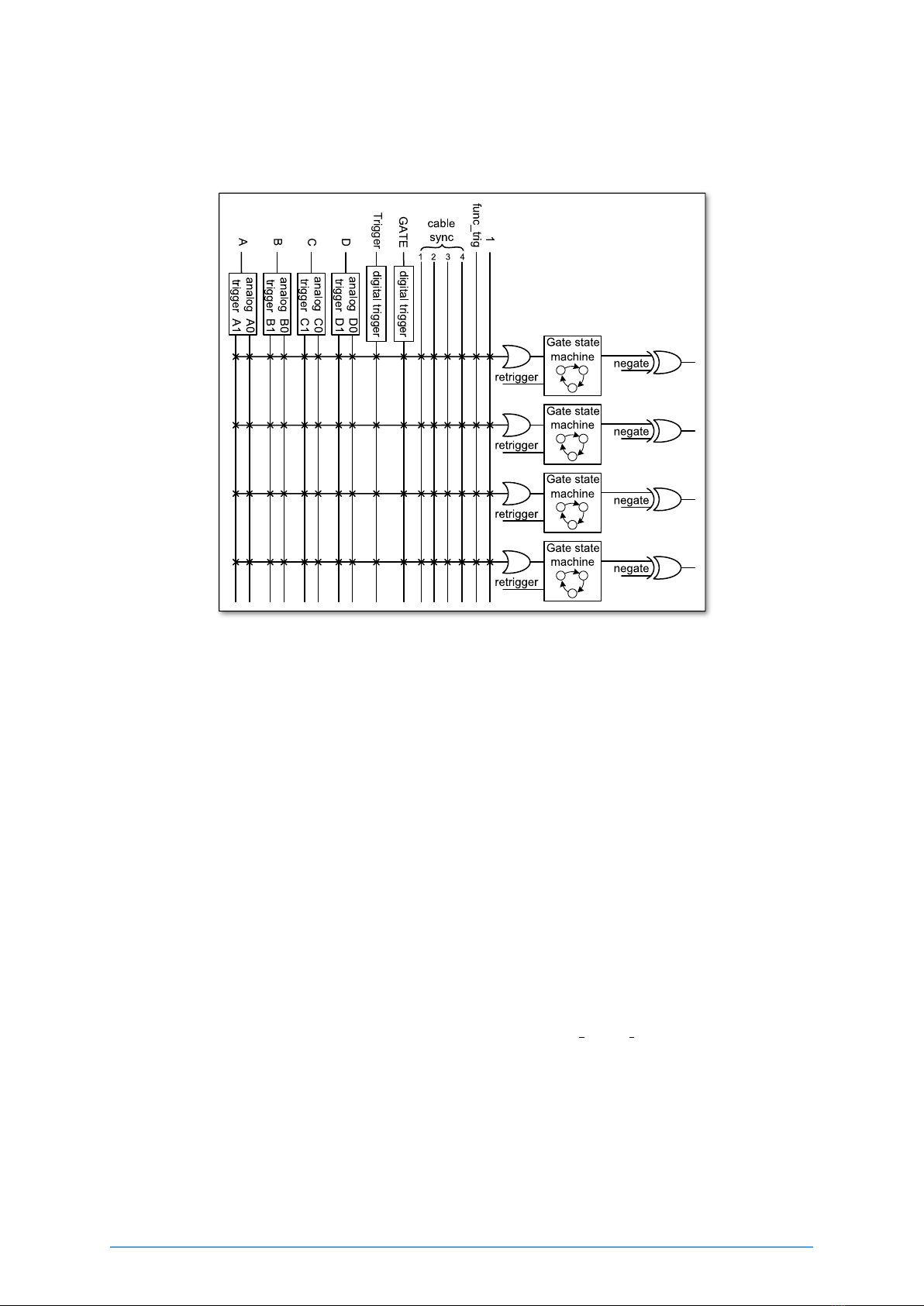
A trigger block can use several input sources:
the 8 trigger decision units of all four ADC channels (Figure 2.16 on page 13)
the GATE input (Figure 2.17 on page 13)
the Trigger input (Figure 2.17 on page 13)
a function trigger providing random or periodic triggering (Section 2.4.5 on page 18)
triggers originating from other cards connected with the sync cable or from the Ndigo
Extension card (BUS0, BUS1, BUS2, BUS3)
A second set of trigger units for the digital inputs Trigger, GATE, BUS0, BUS1, BUS2,
and BUS3 that is set in hardware to positive edge triggering. This set of triggers is not
available as inputs for the gate blocks.
Trigger inputs from the above sources can be concatenated using logical “OR” (Figure 2.19
on page 14) by setting the appropriate bits in the trigger blocks source mask.
Triggers can be fed into the gate blocks described on page 15 (Figure 2.20). Gate blocks can
be used to block writing data to the FIFO. That way, only zero suppressed data occurring when
the selected gate is active is transmitted. This procedure reduces PCIe bus load even further
(Figure 2.20).
precursor = 6 length = 12
total length = 19
threshold
Figure 2.11: Parameters for edge triggering
cronologic GmbH & Co. KG 11 Ndigo5G User Guide
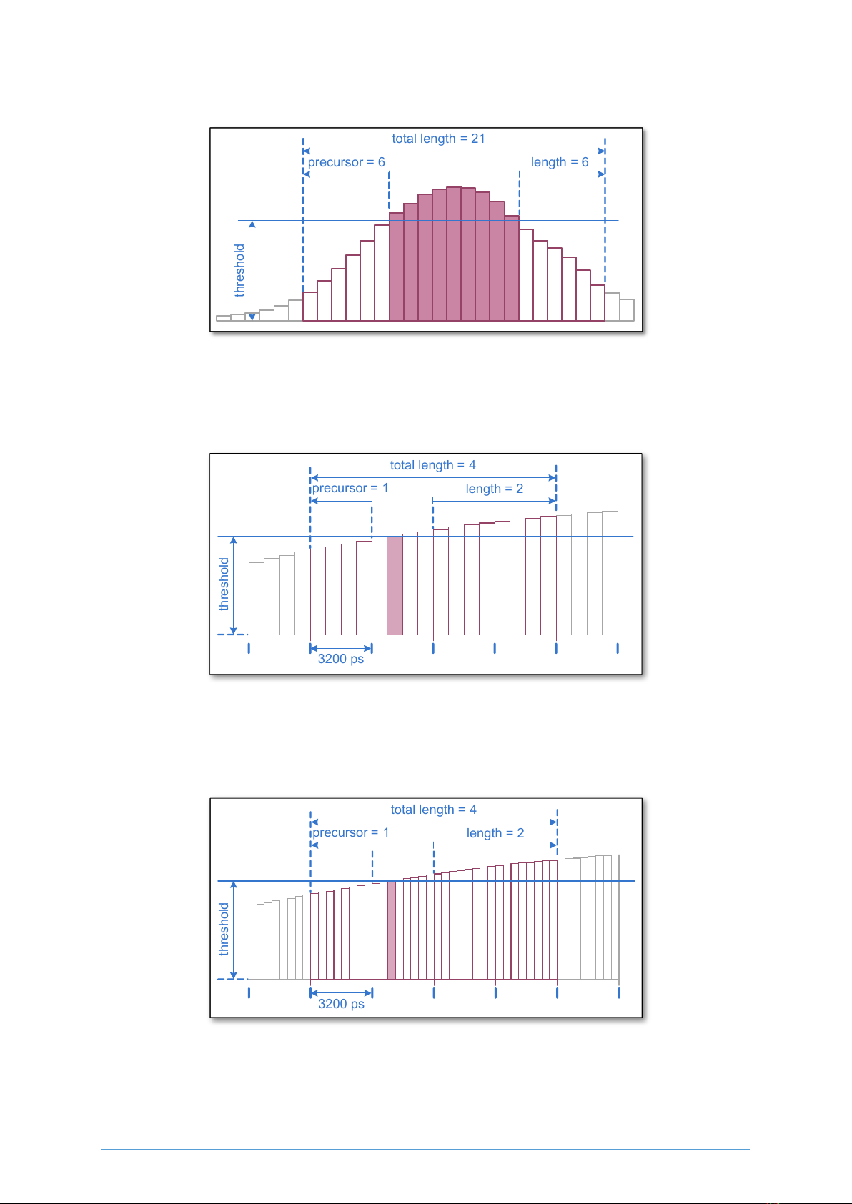
precursor = 6 length = 6
total length = 21
threshold
Figure 2.12: Parameters for level triggering
precursor = 1 length = 2
total length = 4
threshold
3200 ps
Figure 2.13: Triggering in 4 channel mode at 4 samples per clock cycle.
precursor = 1 length = 2
total length = 4
threshold
3200 ps
Figure 2.14: Triggering in 2 channel mode at 8 samples per clock cycle.
cronologic GmbH & Co. KG 12 Ndigo5G User Guide

precursor = 1 length = 2
total length = 4
threshold
3200 ps
Figure 2.15: Triggering in 1 channel mode at 16 samples per clock cycle.
rising
sample data
threshold
Z-1
edge
trigger 1
rising
threshold
Z-1
edge
trigger 2
Figure 2.16: From the ADC inputs, a trigger unit creates an input flag for the trigger matrix.
Each digitizer channel (A, B, C, D) has two trigger units.
rising
Z-1
edge
input
Figure 2.17: The digital inputs Trigger, GATE, BUS0, BUS1, BUS2 and BUS3 have simpler
trigger units.
cronologic GmbH & Co. KG 13 Ndigo5G User Guide

enable
extension input
ignore_cable
cable sync
Figure 2.18: The extension block combines signals from the optional extension board and the
sync cable.
A
B
C
D
trigger_
block[0]
trigger_
block[1]
trigger_
block[2]
trigger_
block[3]
Gates
bus[0]
bus[1]
bus[2]
bus[3]
to cable sync
timestamp
channel
func_trig
1
analog
trigger
analog
trigger
analog
trigger
analog
trigger
Trigger
GATE digital
trigger
digital
trigger
gate
gate_pe
tdc_pe
tdc
A0
A1
B0
B1
C0
C1
D0
D1
digital
trigger bus1
bus1_pe
extension
block
sync1
ext1
digital
trigger bus0
bus0_pe
extension
block
sync0
ext0
digital
trigger bus3
bus3_pe
extension
block
sync3
ext3
digital
trigger bus2
bus2_pe
extension
block
sync2
ext2
Figure 2.19: Trigger Matrix: The trigger signals of each ADC channel, the Triggerinput, the
GATE input or the sync cable can be combined to create a trigger input for each
trigger block. The four gate signals can be used to suppress triggers during certain
time frames.
cronologic GmbH & Co. KG 14 Ndigo5G User Guide
2.4.4 Gating Blocks
Trigger
Figure 2.20: Gating Blocks: Each gating block can use an arbitrary combination of inputs to
trigger its state machine. The outputs can be individually inverted and routed to
the AND-gate feeding the trigger blocks.
To decrease the amount of data transmitted to the PC, Ndigo5G includes 4 independent gate
and delay units. A gate and delay unit creates a gate window starting at a specified time after
a trigger, closing the window at gate stop. Both timing values — gate start and gate stop —
must be set as multiples of 3.2ns.
Trigger blocks can use the gate signal to suppress data acquisition: Only data that fulfills
zero suppression specifications occurring in an active gate window is written to the PC.
As input, any trigger from the 4 trigger blocks, the GATE and Trigger inputs, a trigger from
a connected board and the function generator can be used.
The retrigger feature will create a new gate if a trigger occurs during an active gate window.
The gate signal can be inverted, causing an active gate to close for a time defined by the user.
The parameters of a gating block are set in Structure ndigo gating block described on page
36.
Figure 2.21 shows the functionality of the gate timing and delay unit. Active gate time is
marked in green.
cronologic GmbH & Co. KG 15 Ndigo5G User Guide
This manual suits for next models
1
Table of contents
Popular Motherboard manuals by other brands


V-tech
V-tech ATI A3 + ALI M1535D+ Technical reference booklet

PEmicro
PEmicro Cyclone MAX Getting started guide

IR-Tec
IR-Tec OS-NET SRP-281 Operation instructions

PCchips
PCchips M758 Plus Series user manual

Contec
Contec GMB-C2165-LLVA user manual

Global American Inc.
Global American Inc. 2808000 user manual