-4-
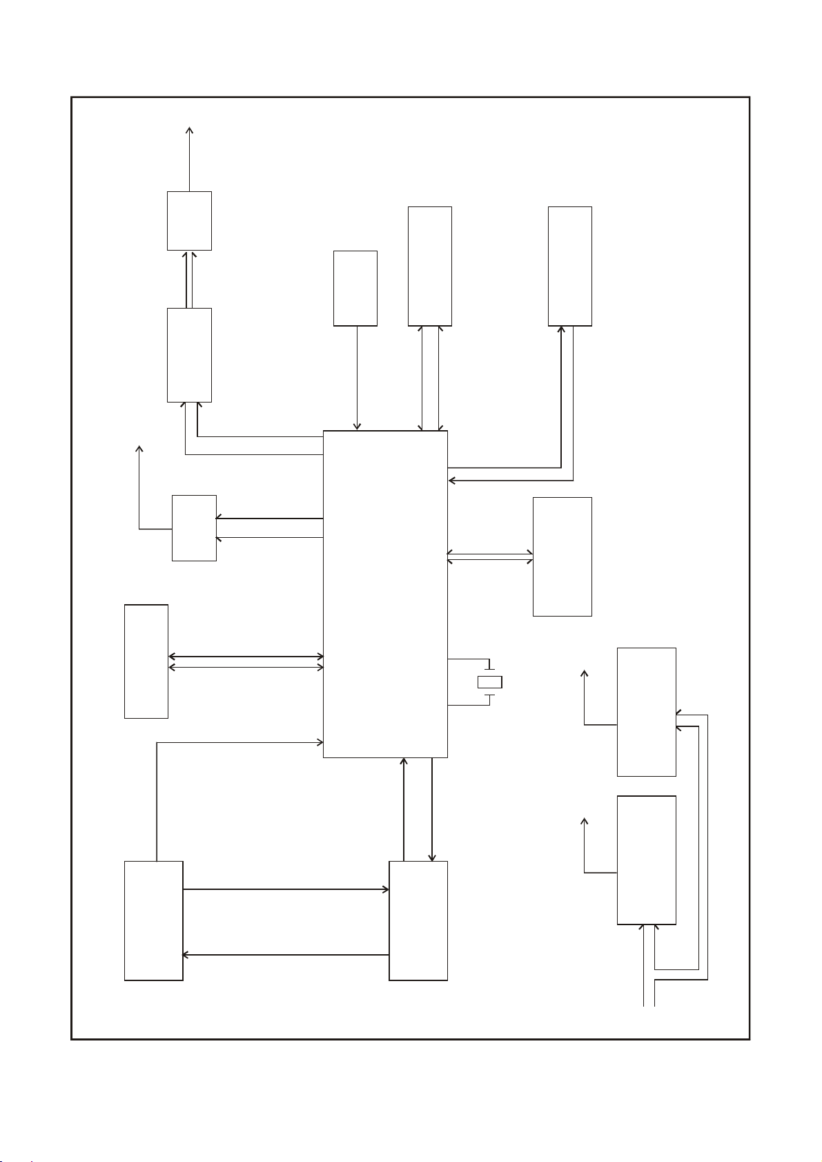
DVD
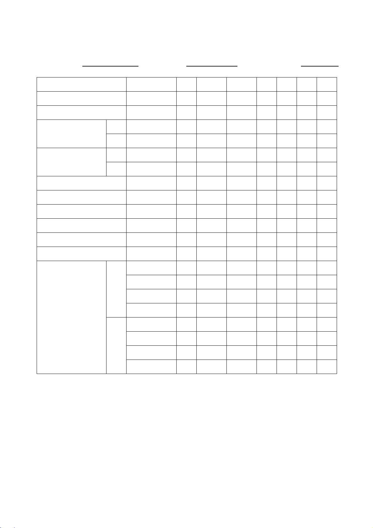
Model No.: LMD-4708GQU Out put: 50mW/16ohm SupplyVoltage:
Description Condition Unit
Limit Nominal
Video Signal Level Vp-p
0.7±0.1
0.7
SYNC Level Vp-p
0.3±0.1
0.3
Video out level
75% color
bar/75ohm Vp-p
1.0±0.2
1
Video out level(Unload) 75% color bar
Vp-p
2.0±0.2
2
CD 1KHz/0dB/10K
V2.0±0.2
2
Audio out level DVD
1KHz/0dB/10K V2.0±0.2
2
20Hz dB ≤±3 0
125Hz dB ≤±3 0
10KHz dB ≤±3 0
FREQ RESP (DVD)
(20Hz~20KHz)
20KHz dB ≤±3 0
Signal-to-noise radio Infinityzere/-dB/L&R
dB 60 60
Audio distortion&noise (DVD) 1KHz/0dB/L&R
dB ≤-65 -65
Dynamic range (DVD) 1KHz/-60dB dB 85 85
R/L Cross sound (DVD) 1KHz/0dB/L&R
dB 45 45
1KHzChannel unbalance (DVD)
1KHz/0dB/L&R
dB ≤3 0
Power Consumption StandbyW00
DC 9V Rating W ≤12 ≤12
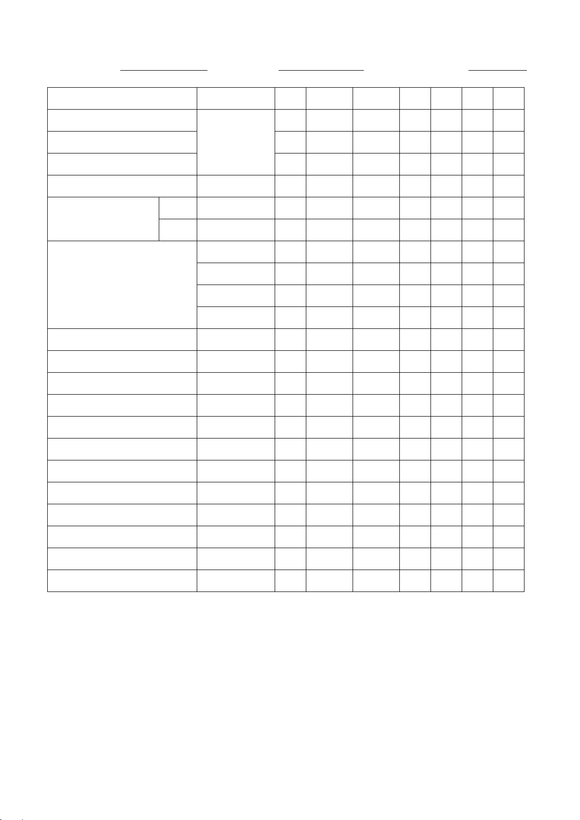
ECC EntircityA BEX TDV-552
um
100 100
Scratch A BEX TDV-541
mm
1.6 1.6
Blackdot A BEX TDV-545
mm
ф0.8
0.8
Finger Print A BEX TDV-545
um
ф65
65
Vertical deviation A BEX TDV-533
mm
0.6 0.6
Note: Nominal specs represent the designspecs. All units should be able toapproximate these. Somewill
exceed andsomemaydropslightlybelowthese specs. Limit specs represent the absolute worst condition that
might still be considered acceptable. In no case should a unit fail to meet limit specs.