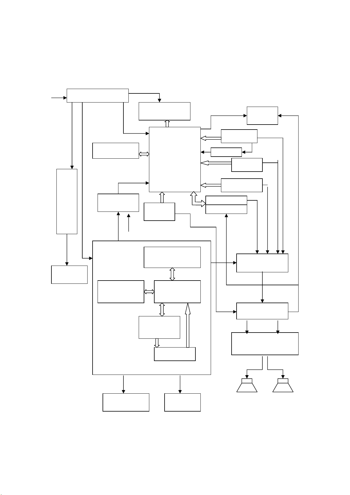
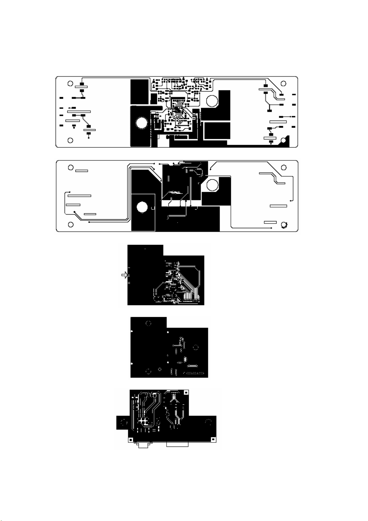
DAEWOO ELECTRONICS DSL-19M1WCD User manual

DSL-19M1WCD
S/M NO. : DLV19M1WCD
LCD COMBO

LTD-61915E SERVICE MANUAL
CONTENT
PART 1:Brief Introduction Of The LTD-61915E
◆ Schematic Diagram
◆ Printed Circuit
PART 2:Exploded view
PART 3:Key Ics And Assemblies
PART 4: Detailed Circuit
◆ Main Board
◆ DVD Board
◆ HI-voltage Board
PART 5: Parts List
PART6: Debug Procedure

FLI8125
Decoder
&
Scaler
Panel
19” TFT LCD
PC IN
AV IN
TUNER
DVD
AT49BV040B
FLASH
POWER SUPPLY
Part 1 Brief Introduction Of The LTD-61915E
Schematic Diagram
12V IN
5V
12V
Composite LR
12V 5V
LVDS
3.3V 1.8V
RGB L R
Hsync Vsync
Composite LR
YC LR
Composite
SIF LR
LR
YPbPr
LR
L R
SVIDEO IN
CD4052
audio switch
TDA1517P
audio power amplify
MXX29LV160BT
FLASH
MT1389HD
Decoder
K4S641632H
SDRAM
BA5494
Motor Driver
LOARDER
74LVC125
FSAV330
video switch
MSP3415G
sound
p
rocesso
r
I
N
V
E
R
T
E
R
4 CCFL
b
ackli
g
h
t
MS, SD, MMS
Interface USB
Interface
AV OUT
SCART
IN
SCART OUT
L R

Printed Circuit
Main board 3678C(Top layer view)

Main board3678C (Bottom layer view)

DVD board 3769C(Top layer view)
DVD board 3769C (Bottom layer view)

HI-voltage Board 3678C(Top layer view)
HI-voltage Board 3678C(Bottom layer view)
SD card board3773C(Top layer view)
SD card board3773C(Bottom layer view)
Earphone board3772C(Top layer view)

Earphone board3772C(Bottom layer view)
Remote control head board3921C(Top layer view)
Remote control head board3921C(Bottom layer view)

Part2 Exploded view


Part 3 Key ICs And Assemblies
On Main Board On DVD board
Serial No Position Type Serial no Position Type
1 3U4 FSAV330 1 U1 BA033T
2 8U3 L7808C-V 2 U2 LM1117
3 2U1 AT49BV040B 3 U3 MT1389HD
4 2U3 FLI8125 4 U4 BA5954
5 1U4 FDS9435A 5 U5 BA6208F
6 1U1 AP1510 6 U6 HY57V641620HGT
7 2U2 AT24C32A 7 U7 MX29LV160BT
8 1U2 AP1513S 8 U8 AT24C16
9 8U4 CD4052 9 U9 NJM4558
10 8U2 MSP3415G 10 U10 WM8714
11 9U1 TDA1517P
12 3U5 3U6 3U7
3U11 3U12 PESD5VOL4U
13 1U3 LM1117
14 3U9 PESD5V0L5
15 2U4 74LVC125
On HI-voltage Board
1 IC1 Bit3193
2 Q7,Q8 AP4511M

ICS ON MAIN BOARD
1. FSAV330
Low On Resistance Quad SPDT Wide Bandwidth Video Switch

2. FLI8125
The FLI8125 is a cost-effective, highly-integrated, mixed signal solution for TV and Digital
Video applications. It incorporates a multi-standard video decoder, high-speed triple 8-bit
Analog-to-Digital Converter(ADC),and front end switching. An integrated VBI Slicer adds
Closed Captioning(CC) and Teletext service support, and the built-in microprocessor enables
full system control without external devices.
Features

·PInput
·Pin List
I/O Legend: A = Analog, I = Input, O = Output, P = Power, G= Ground
Table 1: Analog Input Port
Pin Name No. I/O Description
VDD18_A
B
158 AP Analog Power (1.8V) for A & B Channels. Must be bypassed with 0.1uF capacitor to the analog system
ground plane.
NC 159 No Connection. Leave this pin open for normal operation.
GND18_C 160 AG Analog Ground (1.8V Return) for C channel. Must be directly connected to the analog system ground plane
on board.
VDD18_C 161 AP Analog Power (1.8V) for C Channel. Must be bypassed with 0.1uF capacitor to the analog system ground
plane.
ADC_TES
T
162 O Analog Front End Test O/P. Leave this Pin open. Used for factory testing purpose only.
AVDD_AD
C
163 AP Analog Power (3.3V) for ADC. Must be bypassed with 0.1uF capacitor to the analog system ground plane.
AGND 164 AG Analog Ground. Must be directly connected to the analog system ground plane on board.
AGND 165 AG Analog Ground. Must be directly connected to the analog system ground plane on board.
SV1P 166 AI Positive analog sync input for channel 1.
The input has to be AC coupled using a series 20 Ohm resistor and 0.1uF Capacitor network.

GNDS 167 AG Analog Ground. Must be directly connected to the analog system ground plane on board.
A1P 168 AI Positive analog input ‘A’ for channel 1.
The input has to be AC coupled using a series 20 Ohm resistor and 0.1uF Capacitor network.
GNDS 169 AG Analog Ground. Must be directly connected to the analog system ground plane on board.
B1P 170 AI Positive analog input ‘B’ for channel 1.
The input has to be AC coupled using a series 20 Ohm resistor and 0.1uF Capacitor network.
GNDS 171 AG Analog Ground. Must be directly connected to the analog system ground plane on board.
C1P 172 AI Positive analog input ‘C’ for channel 1.
The input has to be AC coupled using a series 20 Ohm resistor and 0.1uF Capacitor network.
AVDD_A 173 AP Analog Power (3.3V) for ADC of Channel-A. Must be bypassed with 0.1uF capacitor to the analog system
ground plane.
AN 174 AI Negative analog input ‘A’ for channels 1 through 4.
This acts as the return Path for the Sources connected to Channel-A Inputs. This has to be AC coupled
using a series 20 Ohm resistor and 0.1uF Capacitor network to Analog Ground Plane on board.
AGND 175 AG Analog Ground. Must be directly connected to the analog system ground plane on board.
SV2P 176 AI Positive analog sync input for channel 2.
The input has to be AC coupled using a series 20 Ohm resistor and 0.1uF Capacitor network.
GNDS 177 AG Analog Ground. Must be directly connected to the analog system ground plane on board.
A2P 178 AI Positive analog input ‘A’ for channel 2.
The input has to be AC coupled using a series 20 Ohm resistor and 0.1uF Capacitor network.
GNDS 179 AG Analog Ground. Must be directly connected to the analog system ground plane on board.
B2P 180 AI Positive analog input ‘B’ for channel 2.
The input has to be AC coupled using a series 20 Ohm resistor and 0.1uF Capacitor network.
GNDS 181 AG Analog Ground. Must be directly connected to the analog system ground plane on board.
C2P 182 AI Positive analog input ‘C’ for channel 2.
The input has to be AC coupled using a series 20 Ohm resistor and 0.1uF Capacitor network.
AVDD_B 183 AP Analog Power (3.3V) for ADC of Channel-B. Must be bypassed with 0.1uF capacitor to the analog system
ground plane.
BN 184 AI Negative analog input ‘B’ for channels 1 through 4.
This acts as the return Path for the Sources connected to Channel-B Inputs. This has to be AC coupled
using a series 20 Ohm resistor and 0.1uF Capacitor network to Analog Ground Plane on board.
AGND 185 AG Analog Ground. Must be directly connected to the analog system ground plane on board.
SV3P 186 AI Positive analog sync input for channel 3.
The input has to be AC coupled using a series 20 Ohm resistor and 0.1uF Capacitor network.
VDD18_AB 158 AP Analog Power (1.8V) for A & B Channels. Must be bypassed with 0.1uF capacitor to the analog system
ground plane.
GNDS 187 AG Analog Ground. Must be directly connected to the analog system ground plane on board.
A3P 188 AI Positive analog input ‘A’ for channel 3.
The input has to be AC coupled using a series 20 Ohm resistor and 0.1uF Capacitor network.
GNDS 189 AG Analog Ground. Must be directly connected to the analog system ground plane on board.
B3P 190 AI Positive analog input ‘B’ for channel 3.
The input has to be AC coupled using a series 20 Ohm resistor and 0.1uF Capacitor network.
GNDS 191 AG Analog Ground. Must be directly connected to the analog system ground plane on board.
C3P 192 AI Positive analog input ‘C’ for channel 3.
The input has to be AC coupled using a series 20 Ohm resistor and 0.1uF Capacitor network.
AVDD_C 193 AP Analog Power (3.3V) for ADC of Channel-C. Must be bypassed with 0.1uF capacitor to the analog system
ground plane.
CN 194 AI Negative analog input ‘C’ for channels 1 through 4.
This acts as the return Path for the Sources connected to Channel-C Inputs. This has to be AC coupled
using a series 20 Ohm resistor and 0.1uF Capacitor network to Analog Ground Plane on board.
AGND 195 AG Analog Ground. Must be directly connected to the analog system ground plane on board.
SV4P 196 AI Positive analog sync input for channel 4.
The input has to be AC coupled using a series 20 Ohm resistor and 0.1uF Capacitor network.
GNDS 197 AG Analog Ground. Must be directly connected to the analog system ground plane on board.
A4P 198 AI Positive analog input ‘A’ for channel 4.
The input has to be AC coupled using a series 20 Ohm resistor and 0.1uF Capacitor network.
GNDS 199 AG Analog Ground. Must be directly connected to the analog system ground plane on board.
B4P 200 AI Positive analog input ‘B’ for channel 4.
The input has to be AC coupled using a series 20 Ohm resistor and 0.1uF Capacitor network.
GNDS 201 AG Analog Ground. Must be directly connected to the analog system ground plane on board.
C4P 202 AI Positive analog input ‘C’ for channel 4.
The input has to be AC coupled using a series 20 Ohm resistor and 0.1uF Capacitor network.
AVDD_SC 203 AP Analog Power (3.3V) for ADC of SYNC Channel. Must be bypassed with 0.1uF capacitor to the analog
system ground plane.

SVN 204 AI Negative analog sync input for channels 1 through 4.
This acts as the return Path for the Sources connected to SV Channel Inputs. This has to be AC coupled
using a series 20 Ohm resistor and 0.1uF Capacitor network to Analog Ground Plane on board.
VO_GND 205 AG Analog Ground. Must be directly connected to the analog system ground plane on board.
VOUT2 206 AO Analog VOUT signal
This is the Analog Video Output from the Decoder in the Composite Video format. This can be amplified
and be fed to any video display device.
VDD18_SC 207 AP Analog Power (1.8V) for SYNC Channel. Must be bypassed with 0.1uF capacitor to the analog system
ground plane.
GND18_SC 208 AG Analog Ground (1.8V Return) for SYNC channel. Must be directly connected to the analog system ground
plane on board.
Table 2: Low Bandwidth ADC Input Port
Pin Name No I/O Description
VDDA33_LBADC 1 AP Analog Power (3.3V) for Low Bandwidth ADC Block. Must be bypassed with 0.1uF capacitor.
LBADC_IN1 2 AI Low Bandwidth Analog Input-1. The Input signal connected to this Pin, must be bypassed with a 0.1uF
capacitor and could be in the range of 0V to 3.3V (peak to peak).
LBADC_IN2 3 AI Low Bandwidth Analog Input-2. The Input signal connected to this Pin, must be bypassed with a 0.1uF
capacitor and could be in the range of 0V to 3.3V (peak to peak).
LBADC_IN3 4 AI Low Bandwidth Analog Input-3. The Input signal connected to this Pin, must be bypassed with a 0.1uF
capacitor and could be in the range of 0V to 3.3V (peak to peak).
LBADC_IN4 5 AI Low Bandwidth Analog Input-4. The Input signal connected to this Pin, must be bypassed with a 0.1uF
capacitor and could be in the range of 0V to 3.3V (peak to peak).
LBADC_IN5 6 AI Low Bandwidth Analog Input-5. The Input signal connected to this Pin, must be bypassed with a 0.1uF
capacitor and could be in the range of 0V to 3.3V (peak to peak).
LBADC_IN6 7 AI Low Bandwidth Analog Input-6. The Input signal connected to this Pin, must be bypassed with
LBADC_RTN 8 AG This Pin provides the Return Path for LBADC inputs. Must be directly connected to the analog system
ground plane on board.
VSSA33_LBADC 9 AG Analog Ground for Low Bandwidth ADC Block. Must be directly connected to the analog system ground
plane on board.
Table 3: RCLK PLL Pins
Pin Name No I/O Description
GND_RPLL 11 DG Digital GND for ADC clocking circuit. Must be directly connected to the digital system ground plane.
VDD_RPLL_18 12 DP Digital power (1.8V) for ADC digital logic. Must be bypassed with capacitor to Ground Plane.
VBUFC_RPLL 13 O Test Output. Leave this Pin Open. This is reserved for Factory Testing Purpose.
AGND_RPLL 14 AG Analog ground for the Reference DDS PLL. Must be directly connected to the analog system ground
plane.
XTAL 15 AO Crystal oscillator output.
TCLK 16 AI Reference clock (TCLK) from the 14.3MHz crystal oscillator.
AVDD_RPLL_33 17 AP Analog Power (3.3V) for RCLK PLL. Must be bypassed with 0.1uF capacitor.
Table 4: Digital Video Input Port
Pin Name No I/O Description
VID_CLK_1 153 I Video port data clock input meant for Video Input – 1. Up to 75Mhz
[Input, 5V-tolerant]
VIDIN_HS 122 I When Video Input – 1 is in BT656 Mode, this Pin acts as Horizontal Sync Input for Video Input – 2.
OR when Video Input – 1 is in 16 Bit Mode this Pin acts as Horizontal Sync Input for Video Input – 1.
OR this Pin acts as Horizontal Sync Input for 24 Bit Video Input
VIDIN_VS 121 I When Video Input – 1 is in BT656 Mode, this Pin acts as Vertical Sync Input for Video Input – 2.
OR when Video Input – 1 is in 16 Bit Mode this Pin acts as Vertical Sync Input for Video Input – 1.
OR this Pin acts as Vertical Sync Input for 24 Bit Video Input
VID_DATA_IN_0
VID_DATA_IN_1
VID_DATA_IN_2
VID_DATA_IN_3
VID_DATA_IN_4
VID_DATA_IN_5
VID_DATA_IN_6
VID_DATA_IN_7
135
136
137
138
139
140
141
142
IO Input YUV data in 8-bit BT656 of Video Input – 1
[Bi-Directional, 5V-tolerant]
OR Input Y Data in case of 16 Bit Video Input (CCIR601) of Video Input – 1
OR Input Red Data in case of 24 Bit Video Input

Pin Name No I/O Description
VID_DATA_IN_8
VID_DATA_IN_9
VID_DATA_IN_10
VID_DATA_IN_11
VID_DATA_IN_12
VID_DATA_IN_13
VID_DATA_IN_14
VID_DATA_IN_15
145
146
147
148
149
150
151
152
IO Input Pr / Pb Data in case of 16 Bit Video Input (CCIR601) of Video Input – 1
OR Input Green Data in case of 24 Bit Video Input
VID_DATA_IN_16
VID_DATA_IN_17
VID_DATA_IN_18
VID_DATA_IN_19
VID_DATA_IN_20
VID_DATA_IN_21
VID_DATA_IN_22
VID_DATA_IN_23
123
124
125
128
129
130
131
132
IO Input Blue Data in case of 24 Bit Video Input
OR Video Input – 2 in 8-bit with Embedded Sync / Separate Sync Sync in which case
VID_DATA_IN_16 acts as the LSB of the 8-bit Video input and VID_DATA_IN_23 acts as the MSB of
the 8-bit Video input.
VID_CLK2 118 I Video port data clock input meant for Video Input – 2. Up to 75Mhz
[Input, 5V-tolerant]
VID_DE/FLD 115 I Video Active Signal Input or the Field Signal Input from external Digital Video Source.
Note: In case of Multiple Digital Video Input Sources, only one source could be in 8-Bit with
embedded Sync (BT656 mode) format.
Table 5: System Interface
Pin Name No I/O Description
RESETn 10 I Hardware Reset (active low) [Schmitt trigger, 5v-tolerant]
Connect to ground with 0.01uF (or larger) capacitor.
TEST 20 I For normal mode of operation connect this Pin to Ground.
GPIO15 21 IO This pin is available as a general-purpose input/output port. Also it is optionally programmable to
give out the external chip select signal meant for external SRAM. Refer to note below.
HSYNC2 22 I Horizontal Sync signal Input-2. Used when Analog RGB component signal carries separate
HSYNC signal.
VSYNC2 23 I Vertical Sync signal Input-2. Used when Analog RGB component signal carries separate VSYNC
signal.
HOST_SCLK 24 IO Host input clock or 186 UART Data In or JTAG clock signal.
[Input, Schmitt trigger, 5V-tolerant]
HOST_SDATA 25 IO Host input data or 186 UART Data Out or JTAG mode signal.
[Bi-directional, Schmitt trigger, slew rate limited, 5V-tolerant]
DDC_SCLK 26 IO DDC2Bi clock for VGA Port [internal 10KΩpull-up resistor]
DDC_SDATA 27 IO DDC2Bi data for VGA Port [internal 10KΩpull-up resistor]
MSTR_SCLK 30 O Clock signal from Master Serial 2 Wire Interface Controller
MSTR_SDATA 31 IO Data signal meant for Master Serial 2 Wire interface Controller
TCK 34 IO This Pin accepts the Input Clock signal in case of Boundary Scan Mode.
TDI 35 IO This Pin accepts the Input Data signal in case of Boundary Scan Mode.
TMS 36 IO This Pin accepts the Input Test Mode Select signal in case of Boundary Scan Mode.
TRST 37 IO This Pin accepts the Boundary Scan Reset signal in case of Boundary Scan Mode.
GPIO6/IRin 38 IO Input from Infra Red Decoder can be connected to this Pin. When not used, this pin is available
as General Purpose Input/output Port.
GPIO7/IRQin 41 IO Input Interrupt Request signal can be connected to this Pin. When not used, this pin is available
as General Purpose Input/output Port.
GPIO8/IRQout 42 IO This Pin will give out the Interrupt Signal to interrupt external Micro. When not used, this pin is
available as General Purpose Input/output Port.
GPIO9/SIPC_SCLK 43 IO This Pin accepts the Clock signal from External Serial 2 Wire interface Bus if FLI8125 is
programmed to be in Slave mode. When not used, this pin is available as General Purpose
Input/output Port.
GPIO10/SIPC_SDATA/
A18
44 IO This Pin acts as the Data I/O signal when used with External Serial 2 Wire interface Bus if
FLI8125 is programmed to be in Slave mode. Or this Pin is programmable to give out Address #
18 from the Internal Micro when used with 512K External Memory. When not used, this pin is
available as General Purpose Input/output Port.
GPIO11/PWM0 47 IO This Pin can be programmed to give out Pulse Width Modulated Output Pulses for external use.
When not used, this pin is available as General Purpose Input/output Port.
GPIO12/PWM1 48 IO This Pin can be programmed to give out Pulse Width Modulated Output Pulses for external use.
When not used, this pin is available as General Purpose Input/output Port.
GPIO13/PWM2 51 IO This Pin can be programmed to give out Pulse Width Modulated Output Pulses for external use.
When not used, this pin is available as General Purpose Input/output Port.

Pin Name No I/O Description
GPIO14/PWM3/
SCART16
52 IO This Pin can be programmed to give out Pulse Width Modulated Output Pulses for external use.
Or it can be programmed to sense the Fast Blank Input signal from a SCART I/P source. When
not used, this pin is available as General Purpose Input/output Port.
TDO 55 O This Pin provides the Output Data in case of Boundary Scan Mode.
HSYNC1 156 I Horizontal Sync signal Input-1. Used when Analog RGB component signal carries separate
HSYNC signal.
VSYNC1 157 I Vertical Sync signal Input-1. Used when Analog RGB component signal carries separate VSYNC
signal.
101 O Clock Output meant for External OSD Controller
102 O Horizontal Sync Output meant for External OSD Controller
XOSD_CLK 103 O Vertical Sync Output meant for External OSD Controller
XOSD_HS 104 O Field Signal Output meant for External OSD Controller
PD20/B4/GPIO0
PD21/B5/GPIO1
PD22/B6/GPIO2
PD23/B7/GPIO3
86
87
88
89
IO These Pins provide the Panel Data as shown in the TTL Display Interface Table below. These are
available as General Purpose Input / Output Pins when not used as Panel Data.
Table 6: LVDS Display Interface
Pin Name No I/O Description
PBIAS 53 O Panel Bias Control (backlight enable) [Tri-state output, 5V- tolerant]
PPWR 54 O Panel Power Control [Tri-state output, 5V- tolerant]
AVDD_LV_33 56 DP Digital Power for LVDS Block. Connect to digital 3.3V supply.
VCO_LV 57 O Reserved. Output for Testing Purpose only at Factory.
AVSS_LV 58 G Ground for LVDS outputs.
AVDD_OUT_LV_33 59 DP Digital Power for LVDS outputs. Connect to digital 3.3V supply.
CH3P_LV_E 60 O
CH3N_LV_E 61 O
These form the Differential Data Output for Channel – 3 (Even).
CLKP_LV_E 62 O
CLKN_LV_E 63 O
These form the Differential Clock Output Even Channel.
CH2P_LV_E 64 O
CH2N_LV_E 65 O
These form the Differential Data Output for Channel – 2 (Even).
CH1P_LV_E 66 O
CH1N_LV_E 67 O
These form the Differential Data Output for Channel – 1 (Even).
CH0P_LV_E 68 O
CH0N_LV_E 69 O
These form the Differential Data Output for Channel – 0 (Even).
AVSS_OUT_LV 70 G Ground for LVDS outputs.
AVDD_OUT_LV_33 71 DP Digital Power for LVDS outputs. Connect to digital 3.3V supply.
CH3P_LV_O 72 O
CH3N_LV_O 73 O
These form the Differential Data Output for Channel – 3 (Odd).
CLKP_LV_O 74 O
CLKN_LV_O 75 O
These form the Differential Clock Output Odd Channel.
CH2P_LV_O 76 O
CH2N_LV_O 77 O
These form the Differential Data Output for Channel – 2 (Odd).
CH1P_LV_O 78 O
CH1N_LV_O 79 O
These form the Differential Data Output for Channel – 1 (Odd).
CH0P_LV_O 80 O
CH0N_LV_O 81 O
These form the Differential Data Output for Channel – 0 (Odd).
AVSS_OUT_LV 82 G Ground for LVDS outputs.
AVDD_OUT_LV_33 83 DP Digital Power for LVDS outputs. Connect to digital 3.3V supply.

18
Table 7: TTL Display Interface
Pin Name No I/O Description
For8-bitpanels For6-bitpanels
PBIAS 53 O Panel Bias Control (backlight enable) [Tri-state output, 5V- tolerant]
PPWR 54 O Panel Power Control [Tri-state output, 5V- tolerant]
AVDD_LV_33 56 DP Digital Power for TTL Block. Connect to digital 3.3V supply.
VCO_LV 57 O Reserved. Output for Testing Purpose only at Factory.
AVSS_LV 58 G Ground for TTL outputs.
AVDD_OUT_LV_33 59 DP Digital Power for TTL outputs. Connect to digital 3.3V supply.
R0 60 O Red channel bit 0 (Even) Not used.
R1 61 O Red channel bit 1 (Even) Not used.
R2 62 O Red channel bit 2 (Even) Red channel bit 0 (Even)
R3 63 O Red channel bit 3 (Even) Red channel bit 1 (Even)
R4 64 O Red channel bit 4 (Even) Red channel bit 2 (Even)
R5 65 O Red channel bit 5 (Even) Red channel bit 3 (Even)
R6 66 O Red channel bit 6 (Even) Red channel bit 4 (Even)
R7 67 O Red channel bit 7 (Even) Red channel bit 5 (Even)
G0 68 O Green channel bit 0 (Even) Not used.
G1 69 O Green channel bit 1 (Even) Not used.
AVSS_OUT_LV 70 G Ground for TTL outputs.
AVDD_OUT_LV_33 71 DP Digital Power for TTL outputs. Connect to digital 3.3V supply.
G2 72 O Green channel bit 2 (Even) Green channel bit 0 (Even)
G3 73 O Green channel bit 3 (Even) Green channel bit 1 (Even)
G4 74 O Green channel bit 4 (Even) Green channel bit 2 (Even)
G5 75 O Green channel bit 5 (Even) Green channel bit 3 (Even)
G6 76 O Green channel bit 6 (Even) Green channel bit 4 (Even)
G7 77 O Green channel bit 7 (Even) Green channel bit 5 (Even)
B0 78 O Bluechannelbit0(Even) Notused.
B1 79 O Bluechannelbit1(Even) Notused.
B2 80 O Blue channel bit 2 (Even) Blue channel bit 0 (Even)
B3 81 O Blue channel bit 3 (Even) Blue channel bit 1 (Even)
AVSS_OUT_LV 82 G Ground for TTL outputs.
AVDD_OUT_LV_33 83 DP Digital Power for TTL outputs. Connect to digital 3.3V supply.
PD20/B4 86 O Blue channel bit 4 (Even) Blue channel bit 2 (Even)
PD21/B5 87 O Blue channel bit 5 (Even) Blue channel bit 3 (Even)
PD22/B6 88 O Blue channel bit 6 (Even) Blue channel bit 4 (Even)
PD23/B7 89 O Blue channel bit 7 (Even) Blue channel bit 5 (Even)
DEN 90 O Display Data Enable
DHS 91 O Display Horizontal Sync.
DVS 92 O Display Vertical Sync.
DCLK 93 O Display Pixel Clock
PD24 115 O Red channel bit 0 (Odd) Not used.
Pin Name No I/O Description
For8-bitpanels For6-bitpanels
PD25 114 O Red channel bit 1 (Odd) Not used.
PD26 113 O Red channel bit 2 (Odd) Red channel bit 0 (Odd)
PD27 112 O Red channel bit 3 (Odd) Red channel bit 1 (Odd)
PD28 111 O Red channel bit 4 (Odd) Red channel bit 2 (Odd)
PD29 110 O Red channel bit 5 (Odd) Red channel bit 3 (Odd)
PD30 109 O Red channel bit 6 (Odd) Red channel bit 4 (Odd)
PD31 108 O Red channel bit 7 (Odd) Red channel bit 5 (Odd)
PD32 107 O Green channel bit 0 (Odd) Not used.
PD33 106 O Green channel bit 1 (Odd) Not used.
PD34 105 O Green channel bit 2 (Odd) Green channel bit 0 (Odd)
PD35 104 O Green channel bit 3 (Odd) Green channel bit 1 (Odd)
PD36 103 O Green channel bit 4 (Odd) Green channel bit 2 (Odd)
PD37 102 O Green channel bit 5 (Odd) Green channel bit 3 (Odd)
PD38 101 O Green channel bit 6 (Odd) Green channel bit 4 (Odd)
PD39 123 O Green channel bit 7 (Odd) Green channel bit 5 (Odd)
PD40 124 O Blue channel bit 0 (Odd) Not used.
PD41 125 O Blue channel bit 1 (Odd) Not used.
PD42 128 O Blue channel bit 2 (Odd) Blue channel bit 0 (Odd)
PD43 129 O Blue channel bit 3 (Odd) Blue channel bit 1 (Odd)
PD44 130 O Blue channel bit 4 (Odd) Blue channel bit 2 (Odd)
PD45 131 O Blue channel bit 5 (Odd) Blue channel bit 3 (Odd)

19
PD46 132 O Blue channel bit 6 (Odd) Blue channel bit 4 (Odd)
PD47 118 O Blue channel bit 7 (Odd) Blue channel bit 5 (Odd)
Note: In case of 24 Bit TTL Panels the RGB Odd Channel Outputs will not be used. In that case they can be
made available for other purposes as Address & Data from On-Chip Micro or Digital Video Input Data.
Table 8: Parallel/Serial ROM Interface
Pin Name No I/O Description
A17
A16
A15
A14
A13
A12
A11
A10
A9
A8
A7
A6
A5
A4
A3
A2
A1
A0
95
96
100
101
102
103
104
105
106
107
108
109
110
111
112
113
114
115
O 256K x8 PROM Address. These pins also have bootstrap functionality.
For serial SPI ROM interface:
- ROM_ADDR17 will be Serial Clock (ROM_SCLK)
- ROM_ADDR16 will be Serial Data Output (ROM_SDO)
For 512K X 8 PROM, Address Signal A18 is available thru Pin # 44 which is GPIO10.
D7
D6
D5
D4
D3
D2
D1
D0
132
131
130
129
128
125
124
123
IO External PROM data input.
ROM_OEN 118 O External PROM data Output Enable.
ROM_SDI/
ROM_WEN
97 O External PROM data Write Enable (for In-System-Programming of FLASH) or Serial Data Input
(SDI) for SPI ROM interface.
ROM_SCSN/
ROM_CSN
94 O External PROM data Chip Select or Serial PROM Chip Select (ROM_SCSN) for SPI ROM
interface.
Table 9: Digital Power and Ground
Pin Name No I/O Description
RVDD_3.3 32 49 98 116 154 P Ring VDD. Connect to digital 3.3V.
CVDD_1.8 18 28 39 45 84 119 126 133 143 P Core VDD. Connect to digital 1.8V.
CRVSS 19 29 33 40 46 50 85 99 117 120
127 134 144 155
G Chip ground for core and ring.
Table 10: JTAG Boundary Scan
Pin Name No I/O Description
TCK 34 I JTAG Boundary Scan TCK signal
TDO 55 O JTAG Boundary Scan TDO signal
TDI 35 I JTAG Boundary Scan TDI signal. Pad has internal 50K pull-up resistor.
TMS 36 I JTAG Boundary Scan RST signal. Pad has internal 50K pull-up resistor.
TRST 37 I JTAG Boundary Scan TMS signal. Pad has internal 50K pull-up resistor.
Table of contents
Other DAEWOO ELECTRONICS LCD TV manuals

DAEWOO ELECTRONICS
DAEWOO ELECTRONICS DSL-15D1T User manual

DAEWOO ELECTRONICS
DAEWOO ELECTRONICS DLM-42U1 User manual

DAEWOO ELECTRONICS
DAEWOO ELECTRONICS DLM-32C5 User manual

DAEWOO ELECTRONICS
DAEWOO ELECTRONICS DLP-26C2 User manual

DAEWOO ELECTRONICS
DAEWOO ELECTRONICS DLT-42U1GMB User manual

DAEWOO ELECTRONICS
DAEWOO ELECTRONICS DSL-15C1T User manual

DAEWOO ELECTRONICS
DAEWOO ELECTRONICS DSL-15D3 User manual

DAEWOO ELECTRONICS
DAEWOO ELECTRONICS DLN-15D3SHS User manual

DAEWOO ELECTRONICS
DAEWOO ELECTRONICS DLM-26C2 User manual

DAEWOO ELECTRONICS
DAEWOO ELECTRONICS DLP-20J1 User manual