Daewoo DVC-T6300N User manual

SERVICE
MANUAL
DVC-T6300N
For version 2
1.Precautions
2.Reference Information
3.Product Specification
4.Operating Instructions
5.Disassembly and Reassembly
6.Troubleshooting
7.Electrical Part List
8. Block Diagram
9. PCB Diagrams
10. Wiring Diagram
11. Schematic Diagrams
12.Oscillograms
.
Component descriptions

2
1) Before returning an instrument to the customer,
always make a safety check of the entire
instrument, including, but not limited to, the
following items:
(1) Be sure that no built-in protective devices are
defective or have been defeated during servicing.
(1) Protective shields are provided to protect
both the technician and the customer. Correctly
replace all missing protective shields, including
any remove for servicing convenience.
(2) When reinstalling the chassis and/or other
assembly in the cabinet, be sure to put back in
place all protective devices, including, but not
limited to, nonmetallic control knobs, insulating
fish papers, adjustment and compartment
covers/shields, and isolation resistor/capacitor
networks. Do not operate this instrument or
permit it to be operated without all protective
devices correctly installed and functioning.
(2) Be sure that there are no cabinet openings
through which adults or children might be able
to insert their fingers and contact a hazardous
voltage. Such openings include, but are not
limited to, excessively wide cabinet ventilation
slots, and an improperly fitted and/or incorrectly
secured cabinet back cover.
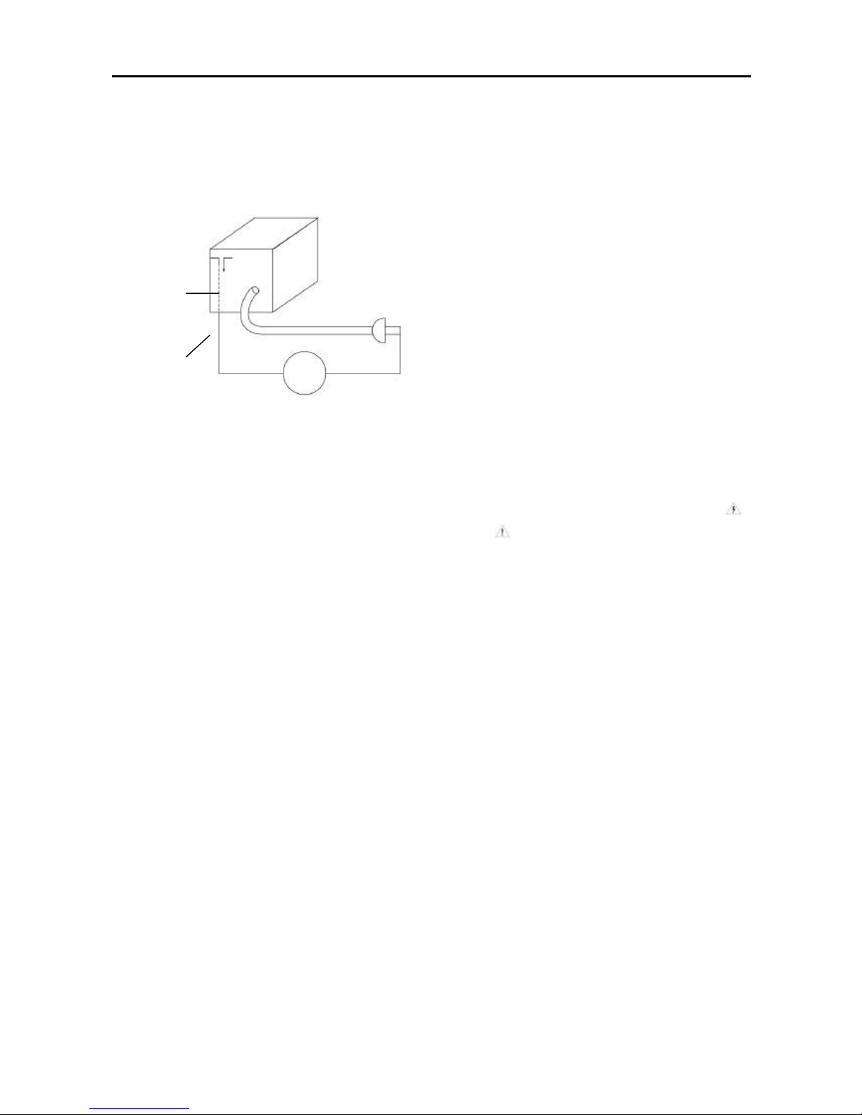
(3) Leakage Current Hot Check-With the
instrument completely reassembled, plug the
AC line cord directly into a 120V AC outlet. (Do
not use a isolation transformer during this test.)
Use a leakage current tester or a metering
system that complies with American National
Standards institute (ANSI) C101.1 Leakage
Current for Appliances and Underwriters
Laboratories (UL) 1270 (40.7). With the
instrument’s AC switch first in the ON position
and then in the OFF position, measure from a
known earth ground (metal water pipe, conduit,
etc.) to all exposed metal parts of the
instrument (antennas, handle brackets, metal
cabinets, screwheads, metallic overlays,
control shafts, etc.), especially and exposed
metal parts that offer an electrical return path
to the chassis.
Any current measured must not exceed 0.5mA.
Reverse the instrument power cord plug in the
outlet and repeat the test. See Fig. 1-1.
Any measurements not within the limits
specified herein indicate a potential shock
hazard that must be eliminated before returning
the instrument to the customer.
Fig. 1-1 AC Leakage Test
(4) Insulation Resistance Test Cold Check-(1)
Unplug the power supply cord and connect a
jumper wire between the two prongs of the plug.
(2) Turn on the power switch of the instrument.
(3) Measure the resistance with an ohmmeter
between the jumpered AC plug and all exposed
metallic cabinet parts on the instrument, such
as screwheads, antenna, control shafts, handle
brackets, etc. When an exposed metallic part
has a return path to the chassis, the reading
should be between 1 and 5.2 megohm. When
there is no return path to the chassis, the
reading must be infinite. If the reading is not
Device
Under
Test
Also test with Plug
reserved (Using AC
adapter Plug as
required)
2-Wire Cord
(Reading
should not
be above
0.5mA)
Test all
exposed Meter
Surfaces
Earth Ground
1. Precautions
1-1 Safety Precautions

3
(5) within the limits specified, there is the possibility
of a shock hazard, and the instrument must be
re-pared and rechecked before it is returned to
the customer. See Fig. 1-2.
Fig. 1-2 Insulation Resistance Test
2) Read and comply with all caution and safety
related notes non or inside the cabinet, or on the
chassis.
3) Design Alteration Warning-Do not alter of add to
the mechanical or electrical design of this
instrument. Design alterations and additions,
including but not limited to, circuit modifications
and the addition of items such as auxiliary audio
output connections, might alter the safety
characteristics of this instrument and create a
hazard to the user. Any design alterations or
additions will make you, the service, responsible
for personal injury or property damage resulting
there from.
4) Observe original lead dress. Take extra care to
assure correct lead dress in the following areas:
(1) near sharp edges, (2) near thermally hot
parts (be sure that leads and components do not
touch thermally hot parts), (3) the AC supply, (4)
high voltage, and (5) antenna wiring. Always
inspect in all areas for pinched, out-of-place, or
frayed wiring, Do not change spacing between a
component and the printed-circuit board. Check
the AC power cord for damage.
5) Components, parts, and/or wiring that appear to
have overheated or that are otherwise damaged
should be replaced with components, parts
and/or wiring that meet original specifications.
Additionally determine the cause of overheating
and/or damage and, if necessary, take corrective
action to remove and potential safety hazard.
6) Product Safety Notice-Some electrical and
mechanical parts have special safety-related
characteristics which are often not evident from
evisual inspection, nor can the protection they
give necessarily be obtained by replacing them
with components rated for higher voltage,
wattage, etc. Parts that have special safety
characteristics are identified by shading, an ( )
or a ( ) on schematics and parts lists. Use of a
substitute replacement that does not have the
same safety characteristics as the recommended
replacement part might created shock, fire
and/or other hazards. Product safety is under
review continuously and new instructions are
issued whenever appropriate.
Antenna
Terminal
Exposed
Metal Part ohm
ohmmeter
Servicing Precautions

4
CAUTION : Before servicing Instruments covered
by this service manual and its supplements, read
and follow the Safety Precautions section of this
manual.
Note :If unforeseen circument create conflict
between the following servicing precautions and
any of the safety precautions, always follow the
safety precautions. Remember: Safety First.
1-2-1 General Servicing Precautions
(1) a. Always unplug the instrument’s AC power
cord from the AC power source before (1) re-
moving or reinstalling any component, circuit
board, module or any other instrument
assembly, (2) disconnecting any instrument
electrical plug or other electrical connection,
(3) connecting a test substitute in parallel with
an electrolytic capacitor in the instrument.
b. Do not defeat any plug/socket B+ voltage
interlocks with which instruments covered by
this service manual might be equipped.
c. Do not apply AC power to this instrument
and /or any of its electrical assemblies unless
all solid-state device heat sinks are correctly
installed.
d. Always connect a test instrument’s ground
lead to the instrument chassis ground before
connecting the test instrument positive lead.
Always remove the test instrument ground lead
last.
Note : Refer to the Safety Precautions section
ground lead last.
(2) The service precautions are indicated or printed
on the cabinet, chassis or components. When
servicing, follow the printed or indicated service
precautions and service materials.
(3) The components used in the unit have a
specified flame resistance and dielectric
strength.
When replacing components, use components
which have the same ratings. Components I-
enti-fied by shading, by ( ) or by ( ) in the
circuit diagram are important for safety or for the
characteristics of the unit. Always replace them
with the exact replacement components.
(4) An insulation tube or tape is sometimes used
and some components are raised above the
printed wiring board for safety. The internal
wiring is sometimes clamped to prevent contact
with heating components. Install such elements
as they were.
(5) After servicing, always check that the removed
screws, components, and wiring have been
installed correctly and that the portion around
the serviced part has not been damaged and so
on. Further, check the insulation between the
blades of the attachment plug and accessible
conductive parts.
1-2-2 Insulation Checking Procedure
Disconnect the attachment plug from the AC outlet
and turn the power ON. Connect the insulation
resistance meter (500V) to the blades of the
attachment plug. The insulation resistance between
each blade of the attachment plug and accessible
conductive parts(see note) should be more than 1
Megohm.
Note : Accessible conductive parts include metal
panels, input terminals, earphone jacks, etc.
1-2 Servicing Precautions

5
Electrostatically Sensitive Devices (ESD)
Some semiconductor (solid state) devices can be
damaged easily by static electricity.
Such components commonly are called
Electrostatically Sensitive Devices(ESD). Examples
of typical ESD devices are integrated circuits and
some field-effect transistors and semiconductor
chip components. The following techniques should
be used to help reduce the incidence of component
damage caused by static electricity.
(1) Immediately before handling any semiconductor
components or semiconductor-equipped
assembly, drain off any electrostatic charge on
your body by touching a known earth ground.
Alternatively, obtain and wear a commercially
available discharging wrist strap device, which
should be removed for potential shock reasons
prior to applying power to the unit under test.
(2) After removing an electrical assembly equipped
with ESD devices, place the assembly on a
conductive surface such as aluminum foil, to
prevent electrostatic charge buildup or exposure
of the assembly.
(3) Use only a grounded-tip soldering iron to solder
or unsolder ESD device.
(4) Use only an anti-static solder removal devices.
Some solder removal devices not classified as
“anti-static”can generate electrical charges
sufficient to damage ESD devices.
(5) Do not use freon-propelled chemicals. These
can generate electrical charges sufficient to
damage ESD devices.
(6) Do not remove a replacement ESD device from
its protective package until immediately before you
are ready to install it. (Most replacement ESD
devices are packaged with leads electrically
shorted together by conductive foam, aluminum
foil or comparable conductive materials).
(7) Immediately before removing the protective
materials from the leads of a replacement ESD
device touch the protective material to the
chassis or circuit assembly into which the
device will be installed.
CAUTION : Be sure no power is applied to the
chassis or circuit, and observe all other safety
precautions.
(8) Minimize bodily motions when handling
unpackaged replacement ESD devices.
(Otherwise harmless motion such as the
brushing together of your clothes fabric or the
lifting of your foot from a carpeted floor can
generate static electricity sufficient to damage
an ESD device).
1-3 ESD Precautions

6
*D.C. Power Supply
A 4-pin shrouded, keyed male connector is used to provide the D.C. Power.
The pin assignment is described below.
PIN DC VOLTS
1 +12V
2 GND
3 GND
4 +5V
Figure-1D.C. Power Connector
*Interface Connector
A 39-pin male, unshielded, shrouded, keyed connector are applied.
Please refer to Section 7-2-3 regarding its pin definition.
39 1
40 2
Interface Connector
*Electrical Charateristics
1. Power
1-1. Voltage
+5V DC with ±5% tolerance, less than 100mVp-p Ripple Voltage
+12V DC with ±10% tolerance, less than 150mVp-p Ripple Voltage
1-2. Current
Continuous Reading
+5V DC 500mA (Average)
+12V DC 300mA (Average)
Seeking & Spin up
+5V DC 0.8 A (Maximum)
+12V DC 1.5 A (Maximum)
2. Signal Summary
The physical interface consists of single ended TTL compatible receivers.
2-1-1 DVD ATAPI LOADER (RL-A700)
2. Reference Information
2-1 Component Descriptions

7
3. Connector Pin Definition
Signal Pin I/O Description
CS0 37 IChip select 0
CS1 38 IChip select 1
DA0 35 IDevice address bit 0
DA1 33 IDevice address bit 1
DA2 36 IDevice address bit 2
DASP 39 I/O Device active or slave (device 1) present
DD0 17 I/O Data bus bit 0
DD1 15 I/O Data bus bit 1
DD2 13 I/O Data bus bit 2
DD3 11 I/O Data bus bit 3
DD4 9I/O Data bus bit 4
DD5 7I/O Data bus bit 5
DD6 5I/O Data bus bit 6
DD7 3I/O Data bus bit 7
DD8 4I/O Data bus bit 8
DD9 6I/O Data bus bit 9
DD10 8I/O Data bus bit 10
DD11 10 I/O Data bus bit 11
DD12 12 I/O Data bus bit 12
DD13 14 I/O Data bus bit 13
DD14 16 I/O Data bus bit 14
DD15 18 I/O Data bus bit 15
DIOR 25 II/O read
DIOW_ 23 II/O write
DMARK_ 29 IDMA acknowledge
DMARQ_ 21 ODMA request
INTRQ 31 OInterrupt request
AOCS16 32 OI/O device 16-bit
IORDY 27 OII/O ready
PDIAG_ 34 I/O Passed diagnostics
RESET_ 1IReset
CSEL 28 Cable select
KEY PIN 20 Key pin
GND 2,19,22,24,26,30,40
Component Descriptions

8
*Appendix 1. DSL-710A Block Diagram
*Appendix 2. Key-Components List
ITEM Model Name MAKER
Laser Pickup SF-HD6AVS Sanyo Electric
Spindle Motor RSM-2811G Samhongsa
Feedling Motor RF-300CA-11440 Mabuchi
Loading Motor RF-300CA-11440 Mabushi
Decoder IC M5705 Ali
RF Amp IC SP3721A Ali
Actuator & Motor Drive IC BA5954FP Rohm
Spindle Motor Drive IC BA6664FM Rohm
Spindle
Motor Focus
Coil Track
Coil Sled
Motor Loading
Motor
BA6664FM
Spindle Motor Drive
BA5954FP
4Ch Motor Drive
80C52
System Controller
Flash
Memory
(1Mbit)
MT1366
(RF AMP.)
Laser Driver
Equalizer
Error Gen.
Disc Motor Unit
Laser
Pickup
MT1368
(Decoder/Servo)
ATAPI
Buffer Manager
Demodulator
Error Correction
PLl
Focus & Tracking
Feeding
Loading
DRAM
(4Mbit)
Spindle Motor Signal for CLV
Motor Signal
Actuator Signal
Disc
33.86MHz
5V
GND
GND
12V
I/F
Conn.
Component Descriptions

9
* Recommended Operating Conditions
Item Symbol Min. Typ. Max. Unit
Supply Voltage Vcc 4.75 5.0 5.25 V
High Level Input Voltage VIH 2.0 -Vcc V
Low Level Input Voltage VIL 0-0.8 V
2-1-2 Fiber Optic Transmitting Module for Digital Audio Equipments (VST5B))
Component Descriptions

10
2-1-3 NTSC/PAL Digital Video Encoder (AD7170)
Component Descriptions

11
Component Descriptions

12
Component Descriptions

13
* Features
lSingle-chip DVD video decoder in a 208-pin PQFP package
lSupports MPEG-1 system and MPEG-2 program streams
lProgrammable multimedia processor architecture
lCompatible with Audio CD, Video CD, VCD 3.0, and Super Video CD(SVCD)
lDVD Navigation 1
lBuilt-in Content Scrambling System(CSS)
-Audio
lBuilt-in Karaoke key-shift function
lDolbyTM Digital 2-channel downmix audio output for DolbyTM
lDolby Pro Logic
lLinear PCM streams for 24 bit / 96KHz
lConcurrent S/PDIF out and 2-channel audio output
lSensaura Dolby Digital Virtual Surround
lDTS Digital Surround 2-channel downmix stereo output
lS/PDIF output for encoded AC-3, DTS Digital output or Linear PCM
-Peripheral
lGlueless unterface to DVD loaders (ATAPI or A/V bus I/F)
lBidirectional I2C audio interface
lDirect servo / loader interface
l8 general-purpose auxiliary ports
lSingle 27MHz clock input
-Smart Technology
lSmartZoomTM for motion zoom & pan
lSmartScaleTM for NTSC to PAL conversion and vice versa
lSmartStreamTM for video error concealment
Component Descriptions
2-1-4 DVD Processor Chip (Swan-2TM ES4318)

14
*Functional Description
Component Descriptions

15
Component Descriptions
* Pinout Diagram

16
*Pin Description
Name Number I/O Definition
VCC
1, 9, 18, 27, 35, 44, 51, 59, 68, 75,
83, 92, 99, 104, 111,121, 130,
139, 148, 157, 164, 172, 183,
193, 201
I3.65 V ± 150 mv.
LA[21:0] 23:19,16:10,7:2,207:204 ODevice address output.
VSS 8,17,26,34,43,52,60,67,76,84,91
,98,103112,120,129,138,147,15
6,163,171,177,184,192,200,208 IGround.
RESET# 24 IReset input, active low.
TDMDX OTDM transmit data
RSEL 25 I
ROM Select
RSEL Selection
016-bit ROM
1 8-bit ROM
TDMDR 28 ITDM receive data.
TDMCLK 29 ITDM clock input.
TDMFS 30 ITDM frame synch.
TDMTSC# 31 OTDM output enable, active low.
TWS
SEL_PLL1 32 O
IAudio transmit frame sync.
Select PLL1.
TSD
SEL_PLL0 33 O
I
Audio transmit serial data port.
Select PLL0.
SEL_PLL2 SEL_PLL0 Clock Output
0 0 2.5 x DCLK
0 1 3 x DCLK
1 0 3.5 x DCLK
1 1 4 x DCLK
SEL_PLL2 36 Select PLL2. See the table for pin number 33.
MCLK 39 I/O Audio master clock for audio DAC.
TBCK 40 I/O Audio transmit bit clock.
SDIF_DOBM 41 OS/PDIF (IEC958)Format Output.
RSD 45 IAudio receive serial data.
RWS 46 IAudio receive frame synch.
RBCK 47 IAudio receive bit clock.
APLLCAP 48 IAnalog PLL Capacitor.
XIN 49 ICrystal input.
XOUT 50 OCrystal output.
DMA[11:0] 66:61, 58:53 ODRAM address bus.
DCAS# 69 OColumn address strobe, active low.
DOE#
DSCK_EN 70 O
IOutput enable, active low.
Clock enable, active low.
DWE# 71 ODRAM write enable, active low.
DRAS[2:0]# 74:72 ORow address strobe, active low.
DB[15:0] 96:93, 90:85, 82:77 I/O DRAM data bus.
DCS[1:0]# 97, 100 OSDRAM chip select [1:0], active low.
DQM 101 OData input / output mask.
DSCK 102 OClock to SDRAM.
DCLK 105 IClock Input(27MHz).
YUV[7:0] 115:113, 110:106 O8-bit YUV output.
PCLK2XSCN 116 I/O 2X pixel clock.
PCLKQSCN 117 I/O Pixel clock.
1. VSY
NC
H# 118 I/O Vertical synch for screen video interface,
programmable for rising or falling edge, active
low.
Component Descriptions

17
Component Descriptions
Name Number I/O Definition
HSYNCH# 119 I/O Horizontal synch for screen video interface,
programmable for rising or falling edge, active
low.
HD[15:0] 141:140, 137:131, 128:122 OHost data bus
HCS1FX# 152 OHost select 1.
HCS3FX# 153 OHost select 3.
HIOCS16# 151 IDevice 16-bit data transfer.
HA[2:0] 158, 155:154 I/O Host address bus.
VPP 159 IPeripheral protection voltage.
HWR#/DCI_
ACK# 149 I,I Host write/DCI Interface Acknowledge Signal,
active low.
HRD#DCI_C
LK 150 I,I Host read/DCI Interface Clock.
HD[15:0]141:140, 137:131, 128:122 I/O Host data bus.
HWRQ# 142 OHost write request.
HRDQ# 143 OHost read request.
HIRQ 144 I/O Host interrupt.
HRST# 145 OHost reset.
HIORDY 146 IHost I/O ready
HWR# 149 OHost write request.
AUX[7:0] 169:165, 162:160 I/O Auxiliary ports.
LOE# 170 ODevice output enable, active low.
LCS[3:0]# 176:173 OChip select[3:0], active low.
LD[15:0] 197:194, 191:185, 182:178 I/O Device data bus.
LWRLL# 198 ODevice write enable, active low.
LWRHL# 199 ODevice write enable, active low.
NC 37, 38, 42, 203:202 No Connect pins. Leave open

18
* Block Diagram
Component Descriptions
2-1-5 DIGITAL-TO-ANALOG STEREO AUDIO CONVERTER (CS4391)

19
Component Descriptions

20
Component Descriptions
Table of contents
Other Daewoo CD Player manuals