Daewoo DV-K580NZ-T User manual

Service Manual
S/M No. : VK580NTEF0
Jan. 2000
DAEWOO ELECTRONICS CO., LTD.
http : //svc.dwe.co.kr
TIME LAPSE VCR
Model: DV-K580NZ-T

1
TABLE OF CONTENTS
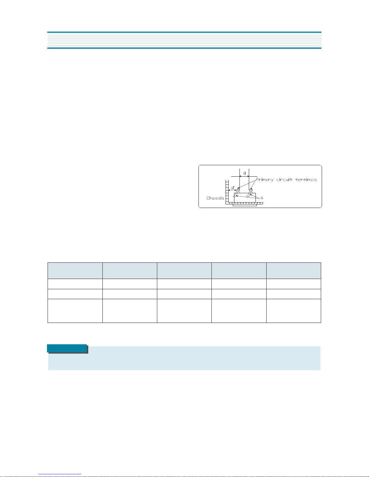
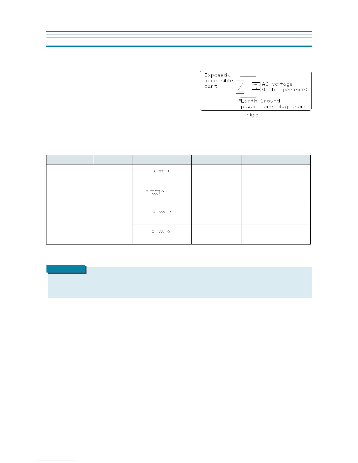
SAFETY&PRECAUTIONS ............................................................................................... 2
EXTERNAL VIEWS ........................................................................................................ 4
FRONT VIEWS FUNCTION ...................................................................................................................4
REAR VIEWS FUNCTION .....................................................................................................................5
ELECTRICAL ADJUSTMENT ........................................................................................... 6
SPECIFICATIONS ....................................................................................................... 14
TIMELAPSE REC/PB SPEED CHART
................................................................................ 15
CIRCUIT OPERATION .................................................................................................. 16
TROUBLE SHOOTING FLOW CHART ............................................................................. 24
POWER CIRCUIT ................................................................................................................................24
SERVO-SYSCON CIRCUIT ...................................................................................................................26
VIDEO CIRCUIT .................................................................................................................................34
AUDIO CIRCUIT .................................................................................................................................38
u-COM PORT DESCRIPTION ....................................................................................... 41
VOLTAGE CHART ....................................................................................................... 44
CIRCUIT DIAGRAM ..................................................................................................... 50
CONNECTION DIAGRAM ..................................................................................................................50
POWER CIRCUIT DIAGRAM ................................................................................................................51
SYSCON CIRCUIT DIAGRAM ..............................................................................................................52
VIDEO CIRCUIT DIAGRAM .................................................................................................................53
HEADAMP CIRCUIT DIAGRAM ............................................................................................................54
OSD CIRCUIT DIAGRAM ....................................................................................................................55
Y/C SEPARATION CIRCUIT DIAGRAM ..................................................................................................56
AUDIO CIRCUIT DIAGRAM .................................................................................................................57
LOGIC CIRCUIT DIAGRAM .................................................................................................................58
TERMINAL CIRCUIT DIAGRAM ............................................................................................................59
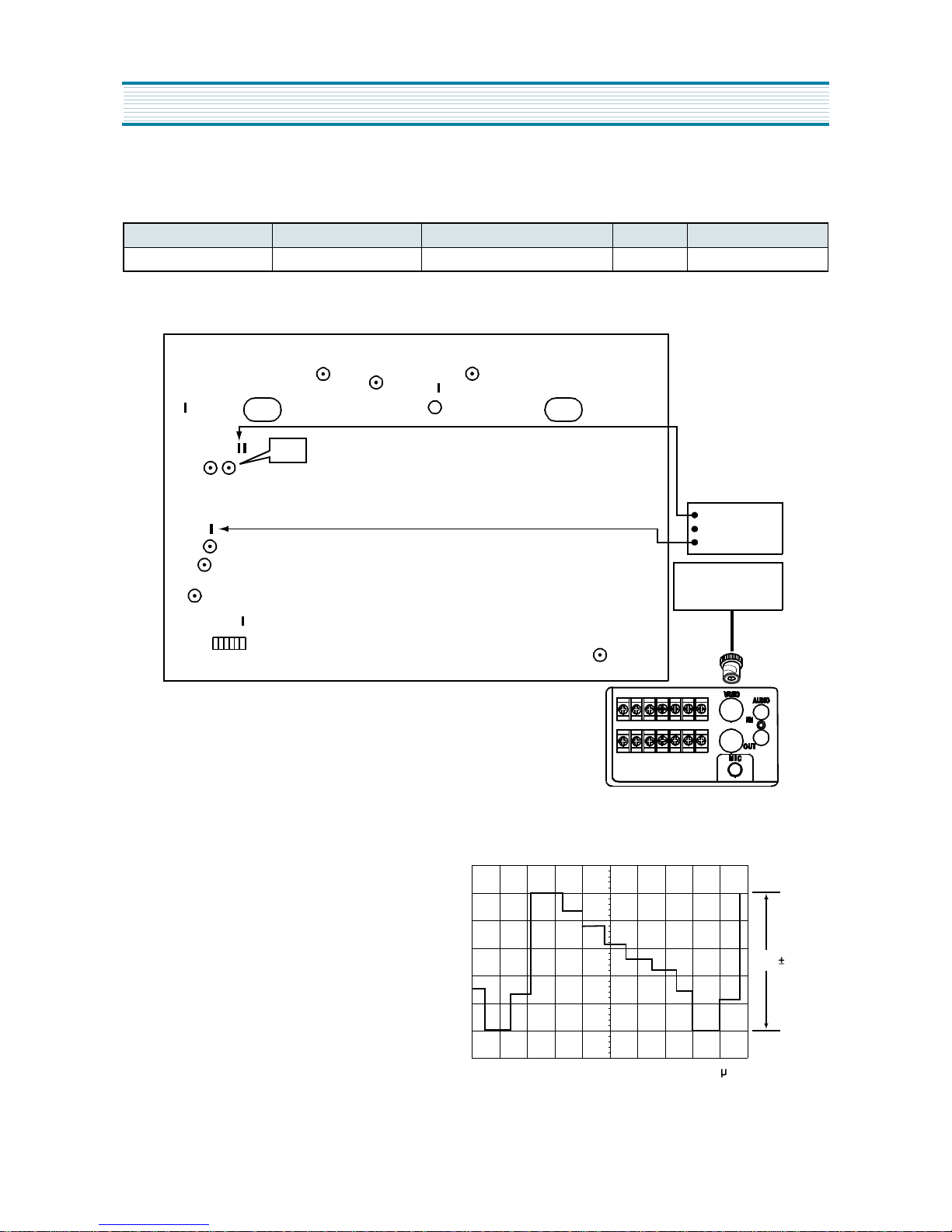
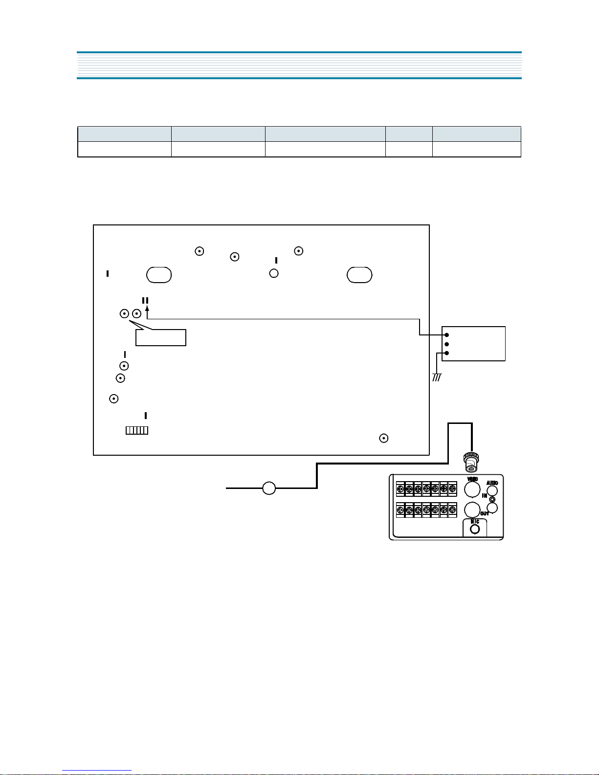
COMPONENTS LOCATION GUIDE ON PCB BOTTOM VIEW ........................................... 60
PCB MAIN .........................................................................................................................................60
PCB UNION .......................................................................................................................................61
DISASSEMBLY ............................................................................................................. 62
PANEL FRONT ASS’Y ...........................................................................................................................62
SET TOTAL ASS’Y .................................................................................................................................63
PACKING ASS’Y .................................................................................................................................64
ELECTRICAL PARTS LIST ............................................................................................... 65

2
SAFETY&PRECAUTIONS
SAFETY CHECK AFTER SERVING
Examine the area surrounding the repaired location for damage or deterioration. Observe that screw, parts and wires
have been returned to original positions. Afterwards, perform the following tests and conform the specified values in order
to verify compliance whit safety standards.
1. Insulation resistance test
Confirm the specified insulation resistance between power cord plug prong and externally exposed parts of the set
(RF terminals, antenna terminals, video and audio input and output terminals, microphone jacks, earphone jacks, etc.)
isgreater than values given in table 1 below.
2. Dielectric strengthen test
Confirm specified dielectric strengthen between power cord
plug prongs and exposed accessible parts of the set
(RF terminals, antenna terminals, video and audio input output
terminals, microphone jack, ear phone jacks, etc.)
is greater than values given table 1.
3. Clearance distance
When replacing primary circuit component, confirm specified clearance distance (d), (d
’
) between soldered terminals,
and between terminals and surrounding metallic parts. See table below.
Rating for selected areas
* : Class model only
AC Line Voltage Region Insulation
Resistance Dielectric
Strength Clearance
Distance(d),(d)
100V Japan
]
1
MΩ
/500VDC 1kV
AC 1min.
]
3
110 to 130V USA &
Canada -900V AC 1min.
]
3.2
* 110 to 130V
200 to 240V
Europe
Australia
Latin America
]
10
MΩ
/500V DC 4kV AC 1min.
]
6(d)
]
8(d
'
)
(a :Power cord)
Thistable isunofficial andfor referenceonly. Besure toconfirm theprecise valuesfor yourparticular countryand locality.
NOTE

3
SAFETY&PRECAUTIONS
4. Leakage current test
Confirm specified or lower leakage current between B(earth
ground, power cord plug prongs) and externally exposed accessi-
ble parts (RF terminals, antenna terminals, video and audio input
output terminals, microphone jacks, earphone jacks, etc.)
Measuring method:(Power ON) Insert load Z between B(earth
ground, power cord plug prongs) and exposed accessible parts.
Use on AC voltmeter to measure across both terminals of load Z.
See figure2 and following table.
Leakage current ratings for selected are as
AC Line Voltage Region Load Z Leakage Current(
i
)Clearance Distance(d),(d’)
100V Japan 1k
Ωi*
1mArms Exposed accessible parts
110 to 130V USA &Canada 15k
µ
F
1k
Ωi*
0.5mArms Exposed accessible parts
110 to 130V
200 to 240V Europe
Australia 2k
Ωi*
0.7mA peak
i*
2mAdc Antenna earth terminals
50k
Ωi*
0.7mA peak
i*
1mAdc Other terminals
This table is unofficial and for reference only. Be sure to confirm the precise values
for your particular country and locality.
NOTE

4
1. FRONT VIEWS FUNCTION
EXTERNAL VIEWS
1) STOP button
2) REC button
3) REC CHECK button
4) EJECT button
5) CASSETTE LOADING DOOR
6) DISPLAY PANEL
7) PLAY button
8) REW button
9) FF button
10)PAUSE/STILL button
11)REMOTE SENSOR
12)REMOCON LOCK SWITCH
13)SET LOCK SWITCH
14)RESET button
15)MENU button
16)SHIFT(
t
) / TRACKING (-) button
17)SHIFT(
U
) / TRACKING (-) button
18)REC/PLAY SPEED (-) button (SET - button)
19)REC/PLAY SPEED (+) button (SET + button)
20)AUDIO ON button
21)DISPLAY button
22)POWER (TIMER ) button
23)COUNTER button
24)CLEAR button

5
EXTERNAL VIEWS
2. REAR VIEWS FUNCTION
1) AC POWER CORD
2) WARNING OUT terminal
3) SERIES IN terminal
4) COM terminal
5) SERIES OUT terminal
6) SW OUT terminal
7) VIDEO OUT jack
8) VIDEO IN jack
9) AUDIO IN jack
10)TAPE END terminal
11)PANIC IN terminal
12)COM terminal
13)ALARM OUT terminal
14)ALARM IN terminal
15)MIC (microphone input) jack
16)AUDIO OUT jack

6
ELECTRICAL ADJUSTMENT
1. SERVO/SYSCON CIRCUIT ADJUSTMENT METHOD
v
VIDEO HEAD SWITCHING POSITION
v
CONNECTION METHOD
v
ADJUSTMENT PROCEDURE
1) Play back the test tape.
2) Settheoscilloscopein the chop mode connect the CH1 to SWpulse(PT501(r)PIN), the CH2 to TJ396(video out) with
CH1 triggering.
3) Adjust R595 for the positive trigger until 6.5
±
0.5H cycle before the vertical SYNC pulse.
Adjustment Part Checking Point Measuring Equipment Mode Test Tape
R595 TJ396
PT501 PIN3 OSCILLOSCOPE Play DN-1 (Color Bar)
TJ396
CH-1
Oscilloscope
CH-2
PT501 R595
CH1 SW PULSE
(PT501 3PIN)
VIDEO OUT
(TJ396)
Vertical SYNC Signal
1H
6.5H 0.5H
Trigger Position

7
ELECTRICAL ADJUSTMENT
2. VIDEO CIRCUIT ADJUSTMENT METHOD
(1) EE LEVEL
v
CONNECTION METHOD
v
ADJUSTMENT PROCEDURE
1) Supply the Color Bar Signal to the VIDEO IN
JACK, and set the VCR to the STOP mode.
2) ConnecttheoscilloscopetoTJ396andtriggerthe
scope with a composite sync signal at TJ302.
3) Adjust R395 to obtain 2.0Vp-p
±
0.2Vp-p
between the SYNC Tip and 100% white level
Adjustment Parts Checking Point Measuring Equipment Test Tape Input Signal
R395 TJ396 Signal Gen. Oscilloscope -Color Bar
2.0V 0.2Vp-p
TJ395
Horizontal :10 s/div
Vertical :0.1V/div
EE
TJ302
CH-1
Oscilloscope
CH-2
SIGNAL
GENERATOR
TJ396
R395

8
ELECTRICAL ADJUSTMENT
(2) PLAYBACK Y-SIGNAL OUTPUT LEVEL
v
CONNECTION METHOD
v
ADJUSTMENT PROCEDURE
1) Playback the COLOR BAR Test tape (DN-1).
2) Connect the oscilloscope to TJ396 and trigger the scope with a composite sync signal at TJ302.
3) Adjust R396 to obtain 2.0
±
0.2Vp-p between the SYNC TIP and 100% white peak level.
Adjustment Parts Checking Point Measuring Equipment Test Tape Input Signal
R396 TJ396 Oscilloscope DN-1 -
TJ302
CH-1
Oscilloscope
CH-2
TJ396
R396
PB-Y
2.0V 0.2Vp-p
TJ396
Horizontal :10 s/div
Vertical :0.5V/div

9
ELECTRICAL ADJUSTMENT
(3) SYNC TIP FREQUENCY
v
CONNECTION METHOD
v
ADJUSTMENT PROCEDURE
1) Set the VCR to STOP mode without Video Signal.(VIDEO IN JACK is shorted with Ground)
2) Connect the frequency counter TJ391.
3) After Inserting Rec Tape REC in SP Mode
4) Adjust R391 to obtain 4.20
±
0.1 MHz.
Adjustment Parts Check Point Measuring Equipment Test Tape Input Signal
R391 TJ391 Frequency Counter - -
SYNC TIP
R391
CH-1
Oscilloscope
CH-2
TJ391
VIDEO IN is shorted with Ground

10
ELECTRICAL ADJUSTMENT
(4) FM DEVIATION
v
CONNECTION METHOD
v
ADJUSTMENT PROCEDURE
1) Supply the Color Bar Signal to the VIDEO IN JACK, and set the VCR to the REC mode.
2) Connect the oscilloscope to TJ396 and trigger scope with a composite sync signal at TJ302.
3) Record the Color Bar Signal for a few minute and
playback it. Then confirm that the playback video
output level (TJ396) is 2.0
±
0.2Vp-p.
4) Adjustas follows ifthe playback videooutputlevel
is not 2.0
±
0.2Vp-p.
4-1) Adjust R392 a little.
4-2) RecordtheColor BarSignalforafewminute
and playback it.
4-3) Confirm the playback video output level.
4-4) Repeat the procedure of 4-1) to 4-3) until
theplaybackvideooutputlevelbecomes2.0
( 0.2Vp-p between sync tip and 100% white
level.
Adjustment Parts Check Point Measuring Equipment Test Tape Input Signal
R392 TJ396 Signal Gen. Oscilloscope Blank Tape Color Bar
2.0V 0.2Vp-p
TJ396
Horizontal :10 s/div
Vertical :0.5V/div
FMDEV
TJ396
TJ302
CH-1
Oscilloscope
CH-2
SIGNAL
GENERATOR
R392

11
ELECTRICAL ADJUSTMENT
(5) C RECORD CURRENT
v
CONNECTION METHOD
v
ADJUSTMENT PROCEDURE
1) Supply the Color Bar Signal to the VIDEO IN JACK, and set the VCR to the REC mode.
2) Connect the oscilloscope to TJ491 and trigger the scope with a composite sync signal at TJ302.
3) Adjust R491 until Y-FM record current is minimized.
4) Adjust R492 until color record current is 130
±
10mVp-p.
Adjustment Parts Check Point Measuring Equipment Test Tape Input Signal
R492 TJ491 Signal Gen. Oscilloscope Blank Tape Color Bar
REC-C
R492 R491 TJ491
TJ302
CH-1
Oscilloscope
CH-2
SIGNAL
GENERATOR
Burst
TJ491 130 10mVp-p

12
ELECTRICAL ADJUSTMENT
(6) Y RECORD CURRENT
v
CONNECTION METHOD
v
ADJUSTMENT PROCEDURE
1) Supply the Color Bar Signal to the VIDEO IN JACK.
2) After Inserting a Rec Tape, Rec in SP MODE.
3) Connect the oscilloscope to TJ491
and trigger the scope with a compos-
ite sync signal at TJ302.
4) Adjust R491 until Y-FM record current
is 500
±
10mVp-p. (Standard SYNC
Tip)
Adjustment Parts Checking Point Measuring Equipment Test Tape Input Signal
R491 TJ491 Signal Gen. Oscilloscope Blank Tape Color Bar
REC-Y
TJ302
CH-1
Oscilloscope
CH-2
SIGNAL
GENERATOR
TJ491
R491
500V 10mVp-p
TJ491

13
ELECTRICAL ADJUSTMENT
3. AUDIO CIRCUIT ADJUSTMENT METHOD
(1) AUDIO RECORD BIAS
v
CONNECTION METHOD
v
ADJUSTMENT PROCEDURE
1) Supply the signal in the OPEN mode.
2) Connect the Audio Level Meter to R01 at the Deck AC Head.
3) After inserting a blank tape, record in SP mode.
4) Adjust R292 to obtain 3 m Vrms .
Adjustment Parts Checking Point Measuring Equipment Condition of Adj. Test Tape
R292 -Audio Level Meter REC mode Blank Tape
R292 REC BIAS
(+)
Audio (-)
Level Meter

14
SPECIFICATIONS
Video Signal system NTSC
REC/PB System Helical scanning system
Tape Width 12.65mm (1/2 inch), VHS
Record system of Luminance Signal Frequency modulation record
Record system of Color Signal Down converted subcarrier phase shift system
Tape Speed (T-120) 2H : 33.35mm/s (SP), 6H : 11.12mm/s(EP),
18H : 3.71mm/s, 36H : 1.85mm/s
Record/Play Time (T-120) SP : 2H/24H/36H, EP : 6H/18H/24H (PLAY)
FF/REWTime (T-120) Within 3 minutes
Video Signal Input 1.0Vp-p 75
Ω
, unbalanced
Video Signal Output 1.0Vp-p 75
Ω
, unbalanced
Luminance Signal to Noise ratio SP : Minimum 45dB, EP : Minimum 41dB
Horizontal resolution Mimimum 350 Lines (B/W), Minimum 300 Lines (Color)
Audio Signal Input Line Input -8.8dBm (1KHz), 47K
Ω
minimum
Audio Signal Output Line Output -7.8dBm (1KHz), 1K
Ω
maximum
Audio Signal to Noise Ratio (A.Weighted) SP : 42dB minimum VHS, EP : 40dB minimum VHS
Audio Frequency Range SP : 0+3, -6dB [100Hz~10KHz] VHS, EP : 0+3, -6dB [100Hz~5KHz] VHS
Distortion SP : 4% maximum VHS, EP : 5% maximum VHS
WOW Flutter SP : 0.3% maximum VHS, EP : 0.4% maximum VHS
Alarm input DC 4~5V (open), DC 0~0.8V (closed) / 5.7k
Ω
Alarm output DC 4~5V (High), DC 0~0.8V (Low) / 5.7k
Ω
Panic input DC 4~5V (open), DC 0~0.8V (closed) / 5.7k
Ω
End output DC 4~5V (High), DC 0~0.8V (Low) / 5.7k
Ω
Warning output DC 4~5V (High), DC 0~0.8V (Low) / 5.7k
Ω
Series input DC 4~5V (High), DC 0~0.8V (Low) / 5.7k
Ω
Series output DC 4~5V (High), DC 0~0.8V (Low) / 5.7k
Ω
Switch output DC 4~5V (High), DC 0~0.8V (Low) / 5.7k
Ω
Common GND
Microphone Input -60dBs 3.5mm mini Jack 10k ohm, unbalanced
Accuracy of Timer Within 2 seconds per day
Compensate Time for Power Fail About 1 Month
Power Supply AC 120V, 60Hz
Power Consumption 17W
Operation Temperature 5
°
C ~ 35
°
C (Humidity : under 80%)
Storage Temperature -20
°
C ~ 60
°
C
Dimension (W x H x D) 360 x 90 x 300 (mm)
Weight Approximate 4.3 Kg (NET)

15
TIMELAPSE REC/PB SPEED CHART
TAPE MODE TAPE SPEED REMARK
REC MODE
T-120
EP24HMODE
IS POSSIBLE
IN PLAY
MODE.
SP 2H 24H 36H
EP 6H 18H
T-160 SP 2.7H 32H 49.5H
EP 8H 24H
PLAY
MODE
T-120 SP 2H 24H 36H
EP 6H 18H 24H
T-160 SP 2.7H 32H 49.5H
EP 8H 24H
AUDIO POSSIBLE NOT POSSIBLE

16
CIRCUIT OPERATION
1. VIDEO PART
1-1) EE MODE
VideoSignal which isoutput from RL902isinput topin37 of IC301 throughOSD IC. Itis amplified 6dBbyAGC, thenitis
output to pin 34. This output signal is output to Video Jack through RL902 of RELAY IC.
1-2) REC MODE
The signal which is input to pin 37 of IC301 is output to pin 3 through IC internal AGC AMP.Ifthis output signal has burst,
it is input to X303 then it separates color signal. If it has not burst, it will pass Y-Emphasis circuit. Each signal is input to
pin 4 then passes 3.5M LPF. Luminance signal is output from pin 40 after FM modulator through MAIN-Emphasis and
color signal is output from pin 15 after low-converted. Each signal is input to pin 12 of IC401 through REC-EQ, then it is
recorded on the tape through HEAD after passing out MIX AMP.
VIDEO IN VIDEO OUT
V.IN
IC001
OSD IC IC301
VIDEO IC
REC EQ
IC401 HEAD AMP
Y-EMPA
CIRCUIT
X303
Y/C
COMB
WITH
BURST
REC C
REC Y

17
CIRCUIT OPERATION
1-3) PB MODE
When playing the tape, the signal which is picked up from the tape is amplified 50 dB. Then luminance signal goes to pin
11 and color signal goes to pin 7 through AGC. Luminance signal of pin 11 is input to pin 39 of IC301 through PB EQ cir-
cuit in order to match playback characteristic. Color signal which is output from pin 7 of IC401 is input to pin 15 of IC301.
PB FM signal is demodulated by IC internal demodulator then it is input to pin 3 after MAIN DE-Emphasis process. If this
output signal has burst, color component will be separated by X303. If it has burst, it is input to pin 4 of IC301 through Y-
emphasis circuit. The signal which is input to pin 4 is output from pin 12 through 3.5M LPF, then it is input to pin 10
through 1H CCD. Color signal which is input to pin 15 passes ACC in order to stabilize level, then 3.58H components will
be extracted by 3.58M BPF through Main Converter.
This 3.58M color signal is input to pin 25 of IC301 in order to eliminate crosstalk, then it will be mixed with luminance sig-
nal after passing CNR circuit. Finally Y/C composite video signal is output from pin 34.
V-OUT
V.IN
IC401
HEAD AMP
X302 IH DLY
X303
Y/C
COMB
Y-EMPH
IC302
IH CCD
IC301
VIDEO IC
PB EQ

18
CIRCUIT OPERATION
2. AUDIO PART
2-1) EE MODE
External AUDIO signal which is input to pin 16 of IC201 is output from pin 22 of IC201 after being amplified through ALC
and Line Amp.
2-2) REC MODE
It will be the REC mode when REC 5V is input to pin 24 of IC201. Input signal will be replaced on the tape through R/P
HEAD after being amplified and modulated with Bias Frequency. Input signal is amplified and frequency compensated by
REC AMP, ie. it means high band compensation in order to match AUDIO HEAD characteristic. Each mode’speakingfre-
quency will be determined by BIAS element (R, L, C) of REC AMP. OSC oscillation frequency is 70KHz sinewave, it will
be used for tape’s full erasing and AUDIO TRACK erasing.
2-3) PB MODE
It will be the PB mode when PB 5V is input to pin 11 of IC201. The signal which is picked up from AUDIO HEAD is input
to EQ AMP, then constant Audio Level will be output by PB LEVEL fixed resistor after each mode is amplified and fre-
quency is compensated.18H AUDIO output level will be compensated with receiving Audio 24H(H) control of u-COM.
Finally this output signal is output through 20KHz LPF.

19
CIRCUIT OPERATION
3. SERVO SYSCON PART
3-1) BLOCK DIAGRAM
DRUM
PG FG AMP CAPSTAN
SPEED CTL
IC501
M37775M5H
u-COM
PROCESSOR
Start end
SENSOR
&
REEL
SENSOR
LOADING
CAM DRIVE
CTL
AMP
VIDEO
BLOCK AUDIO
BLOCK TERMINAL
BLOCK
BACK
UP BATT
Vcc OSC&
RESET
<K580N-T SERVO SYSCON BLOCK>
Table of contents
Other Daewoo VCR System manuals

Daewoo
Daewoo ST263 DVST7L3 User manual

Daewoo
Daewoo Q997K User manual

Daewoo
Daewoo DV-K*84W Series User manual

Daewoo
Daewoo DV- K584N-SJ User manual

Daewoo
Daewoo Video recorder User manual

Daewoo
Daewoo EV-VCR960R User manual

Daewoo
Daewoo DV-T6F4N-PQ User manual

Daewoo
Daewoo VQ230D User manual

Daewoo
Daewoo K-MECHA DECK Operating manual

Daewoo
Daewoo ST200D User manual

Daewoo
Daewoo VQ857D User manual

Daewoo
Daewoo DV-K10DY-QB User manual

Daewoo
Daewoo VQ450D User manual

Daewoo
Daewoo SC242WY-RV Repair manual

Daewoo
Daewoo DV-F46/26N User manual

Daewoo
Daewoo DV4K611DZ-T User manual

Daewoo
Daewoo DVR-1989D User manual

Daewoo
Daewoo ST120W User manual

Daewoo
Daewoo DV-S137WN User manual

Daewoo
Daewoo DV-F24J User manual