demi 10368-144CK User manual

/Kits/10368-144CK_RevG.doc 1 Rev. G 5/9/2023
DEM Part Number 10368-144CK and 10368-144LPCK
10 GHz. Transverter, Low power Transverter, Kit and Complete Kit
Specifications
Frequency:
10368.000 = 144.000 standard
Noise Figure and Gain
< 1.2 dB NF, > 25 dBG
LP: < 3.5 dB NF, >17 dBG
Power Out
> 2.9 Watts.
LP: >10 mw
DC Power
11-16 VDC @ 3 A
LP: < 750 mA
IF Power Input (144 MHz)
1 mW min. - 10Watt max. Adjustable
Options:
Switchable IF frequency control
Preliminary:
This kit and requires knowledge of assembling and testing microwave frequency circuits.
This document refers to some pictures for ease of assembly. A full color PDF picture addendum
document is found on line at: http://01895fa.netsolhost.com/PDF/Manuals/10368-
144CK_RevG_Pics.pdf. This on-line addendum contains extra pictures and details that may help
answer some assembly issues. Within the text of this document, after a description of a procedure,
there may be a number in brackets e.g. [53]. This will refer to a picture on the addendum file on
line.
The 10368-144CK and 10368 -144LPCK is a complete kit version of the 10368-144 High
Power transverter and the 10368-144LP Low Power transverter [1]. In our Complete Kit version,
you receive all three circuit board kits, the 10368K (transverter PCB kit) [2]; the TC [3] and the
DIGILO Synthesizer [4] with a prepped extruded aluminum enclosure, mounting plate and all
necessary hardware and connectors to get you on the air [5]. When completed, you will only need
to supply a TR switch, (SMA relay) [6] Antenna, and a 2-meter transceiver. Originally, the 10368K
PC board kit was designed by W1GHZ and Down East Microwave Inc. but has seen many design
revisions since the original was published by W1GHZ in the 1999 Microwave Update proceedings.
DEMI has refined the design and produced a basic PCB Kit (low power) and two Complete Kits, a
low power and a 3 watt version with all of the interfacing required. This latest Revision includes the
latest LNA designed by W5LUA as the RX input stage in the high power version transverter only.
In this kit, the DEM TC is the interface circuit board that allows the use of up to a 10 watt
144 MHz transceiver. It contains TX and RX level adjustments. It provides all of the DC and RF
switching functions for the transverter actuated by it’s keying circuit that is either PTT-L (to ground)
or PTT-H (+ voltage) on transmit. It also supplies all internal biasing of the transverter and external
switching functions for TR switches, PAs and LNAs. Along with a +9 Volt 1.5 amp regulator to
supply regulated DC power to the transverter and the supporting circuit for the DIGILO that
indicates the external / internal 10 MHz source activation.
The DIGILO synthesizer (the base Local Oscillator) provides a nominal +0 dBm output at
3408.000 MHz for 144 MHz IF operation. The transverter PCB accepts the LO input and multiplies
it to 10224.000 MHz. A test port for tune-up and testing the LO before the signal is injected into
the mixers is available on the transverter board. After mixing, the 10368 MHz signals are tested
through two separate SMA connectors, TX and RX. The TX and RX connectors are spaced
correctly to allow the direct connection of common SMA relay to complete the system and allow the
use of a common antenna connection.

/Kits/10368-144CK_RevG.doc 2 Rev. G 5/9/2023
Kit Building Success Requirements:
This assembly manual assumes that the complete kit version (10368-144CK or 10368-
144LPCK) is being assembled but is also used for the 10368K, the PC board kit version. Use what
is required from this document for the different assembly types. All kits include the PCB, all of its
components, pipe caps, connectors, required hardware, and a CNC machined circuit board
mounting plate [7]. This plate is the key to the success and reliability of the transverter. The plate
is used as a fixture to attach the pipe cap filters to the circuit board. It aligns the pipe caps in the
correct position and then prevents scorching of the PCB while sweating the pipe caps to the PCB.
After assembly of the pipe caps, the mounting plate provides support to the circuit board to prevent
cracking of components, and damaging ground vias. After assembly, the plate provides easy
attachment of standard SMA connectors used for tune-up and final use. There are 2 main
requirements for the completion of this kit. You will need to “Sweat” the pipe caps in place on the
circuit board. This requires a propane torch or a very hot, Hot Air gun! A standard soldering iron
will not work! Second, you will need a way to detect RF power at 3 cm (10 GHz) frequencies to
aid in tune-up. This can be done with a detector diode, a microwave milli-watt power meter or a
spectrum analyzer. The filters need to be tuned after assembly! There are seven of them in
the low power version and nine in the 3 Watt unit. Both transverters will not work without correct
alignment of the filters!
Options:
There are no assembly options for the 10368 transverters detailed in this manual. You are
limited by the transverter’s PCB and supplied components of what version you can assemble. The
manual will describe one way of assembly that will produce a state of the art 10368 MHz
transverter of power level choice. If you wish to experiment with different gain stages and add-on
filters and amplifiers, do so with caution. Modifications should not be attempted without test
equipment that will provide accurate power levels and a spectrum analysis. DEMI will be more
than happy to consult you with any of your modifications, but will only assume full responsibility for
this design if you use the supplied components and assembly procedure. If you decide to stray
from the original design, or assemble the 10368 PCB with your own components, you will assume
the responsibility of the results. We will answer any questions you may have but a repair and/or
alignment by DEMI will only occur if the transverter kit is in stock form! (or at least close!) If
you have any questions about this policy please consult us first before proceeding with your own
design or modification.
Pre-Assembly:
Basic tools that are required besides hand tools such as a #1 Philips head screw driver,
cutting pliers, tweezers, and a minimum of a 25 watt solder iron with a fine wire solder are a
suitable heating device to "Sweat" the pipe cap filters to the transverter's circuit board and a hot
plate to warm the pallet assembly. The aluminum pallet provides excellent structural support of the
PCB but will "heat sink" just about any general consumer's solder iron not allowing clean smooth
solder joints on the surface mount components. Warming the pallet on a hot plate while soldering
the components is the best way.
The TC board which has most of the surface mount work completed requires stuffing the
board with the leaded components and general soldering. It should be assembled per its assembly
document. Some general assembly options may be implemented to it depending on your
requirements. The DEM TC has provisions for an extra RXIF gain stage but only should be utilized
if you require more than 30 dB of system RX gain. The TC allows 1 mW to 10W common or
separate IF input/output that requires the proper configuration during assembly. It’s your choice.

/Kits/10368-144CK_RevG.doc 3 Rev. G 5/9/2023
The regulated or unregulated voltage is switched to supply any additional stages such as a LNA or
power amplifier and the PTT circuit may be mirrored or inverted. The standard document of the TC
has many more details concerning its various options of operation. Please follow it for assembly
and for the completion of the complete kit version of the 10368-144 or 10368-144LP.
The DIGILO can be experimented with before the main transverter assembly is started but
is not required since they are pretested assemblies. You may set the frequency required for your
transverter's conversion scheme and according to the DigiLO's document. It can then be tested for
frequency, output power and spurious if desired with the correct voltage applied and coaxial
connection. Do not operate it without a 50 ohm load on its output. The complete manual is found
on line at our website here: http://01895fa.netsolhost.com/PDF/Manuals/digilor18_9_1.pdf
and includes extra pictorials to illustrate that may help in assembly. Please take time to review
When configuring your system, please note that DEMI can supply a few external options for
the" Low Power" version transverter. If you require a “State of the Art“ noise figure, a 3 cm PHEMT
preamp designed by DEMI and W5LUA can be purchased. It is part number L3-2LNAK (board kit)
or a complete kit version is L3-2LNACK. This is the same circuit design used in the High Power
version transverter. If you decide to increase the output power of your Low Power version
transverter, the 3-3PACK and 3-3PAP 3 watt amplifier is available if you don't have access to the
surplus market of TWTs and other solid-state amplifiers. DEMI also stocks a basic sequencer, and
other accessories that will enable you to complete your 10368 MHz high performance system.
Assembly:
1. Now is the time to get familiar with the kit and verify it is complete. This will also ensure that
you have the correct tools and supplies required to complete the project. It is also time to make
the last minute decision on building the kit or not. A full exchange towards an assembled version
will be provided if you do not go past this step. We want you to be on the band and operating not
struggling to assemble this kit because you were not aware of what it takes to assemble this
microwave transverter. ------ Last chance? OK!
Start by inventorying the parts list. Every part in this kit is important and should be
identified. There are extra chip components packed in the kit, so no need to count them. The
hardware should be sorted and identified. There are some extras there too. However, remember,
No substitutions! Review the schematic and the component placement diagram. Read all of the
assembly steps, 1 - 14, identifying every component used. Some instructions will specify the Low
power (LP), version or the standard High Power (HP) version transverter.
2. Now, let's assemble what we believe is “The most bang for a buck” 10 GHz kit on the
market! Start by examining the circuit board for irregularities. Do not remove the copper foil that is
attached to the backside of the board. This is to provide additional grounding for the 3 watt power
MMIC. During the drilling and plating process, plating or debris may fill the filter probe holes and
prevent the silver pins from being inserted. It is simple enough to use one of the silver pins (extras
provided) and push it through all of the filter probe holes and wiggle it around a bit to be sure it
clears 14 holes total for the LP and 18 for the HP board [8]. Use the component placement
document to identify the filter pin holes. Do not make the holes larger or drill out! Just be sure
the pin fits in all of the holes and they are clear. Also, look very closely for shorts from the ground
plane side and be sure to clear on the top side.
3. Install the PCB to the mounting plate [9]. Place the ground plane side on the pallet and line
up the holes. It only fits one way. Use the 4-40 x 3/16” screws but do not tighten the screws. The
clearance holes in the PCB are purposely made larger so the board can move around slightly on
the mounting plate to allow proper alignment of the SMA connectors and filters. Tighten a few

/Kits/10368-144CK_RevG.doc 4 Rev. G 5/9/2023
random circuit board screws around the pallet and check for alignment with a visual inspection of
the clearance holes in the pallet. They are for the wire and Coax connections on the circuit board.
Adjust the board to center the via pads in the pallet holes then tighten all screws. Now install the
two 4-40 x 9/16” screws, the 1/8” spacers and two 4-40 nuts in the clearance holes on the back
corners of the circuit board[10]. The head of the screw belongs on the pallet. The screw head is
on the pallet, the spacer is between the PCB and the nut. Tighten them and recheck all circuit
board screws.
Then cut the excess material off the board edges with a sharp knife [11]. If you find yourself
cutting too much of the metal of the board, the board is not centered on the pallet. You may use
the pallet as a guide. It is possible that some excess solder from the foil to board attachment is in
the way. If so, remove with the knife or soldering iron tip. When complete, the board edge to pallet
edge will now act as the alignment if the circuit board is ever removed from the pallet. Then clean
up the connector panel edge. Be careful not to cut the copper foil in installed. Again, use the
pallet as a guide.
4. It is now time to prep the pipe caps. All off the pipe caps have been drilled, tapped and
surfaced. Check for remaining burs inside and outside of the caps [12] and then with an abrasive
cloth, (sandpaper, Scotch-Brite) buff-up the open end of the pipe cap, both inside and outside.
The shinier the better the solder will flow [13]. The pallet will hold them in position during
soldering.
5. If you do not wish to solder the pipe caps to the PCB, we can do it for you. Return the pallet
with the PCB mounted and aligned with the pipe caps without the pipe cap hardware. Include
your payment or payment information of $45 USD, which will also cover standard return shipping.
Your pallet will be ready for assembly when returned!
To solder the pipe caps requires a propane gas torch or a very hot "Hot Air System". A
standard solder iron will not do the job! Electronic grade flux (liquid or paste) and electronic grade
solder is also required. Do not use a Acid base flux or solder! Even if you clean the acid flux off
the outside when finished, you cannot clean the inside of the cap and the acid will destroy the
board from the inside out.
6. Starting with any pipe cap, flux the area within the pallet [14] and flux the open end of the
cap and place it into a pallet hole [15]. We prefer to use "No Clean Flux" for the reason stated in
step #5. Do all of the pipe caps. Now heat any cap with the torch being careful not to allow the
flame to come in contact with any bare circuit board [16]. Remove the flame and flow the solder
into the corners of the pallet hole around the pipe cap joint. Re-heat if necessary. Repeat this
process on the rest of the pipe caps until finished. After a few are complete, the soldering becomes
faster because the pallet is now pre-heated.
Do not install the screws in the cap before soldering. The heated gasses inside of the cap
need to escape. Do not apply pressure to the pipe cap while cooling. It will push the PCB away
from the pallet. Then the excess solder will flow between the board and the pallet causing a
“Bump” in the board. Although this is not a disaster, it will cause a problem when soldering the
components to the circuit board. Allow it to cool completely before touching.
7. At the factory, we use “No-Clean” solder exclusively. It disappears with heat with minimal
smoke. We never use any cleaning solution on our assembled products. The concern we have for
kit builders is that after assembly of the pipe caps, excess flux and residue has migrated between
the PCB and the pallet. Depending on the corrosiveness of the flux, this may be a potential
problem. If so we suggest removing the PCB mounting screws and cleaning everything completely

/Kits/10368-144CK_RevG.doc 5 Rev. G 5/9/2023
if you feel that there could be a flux invasion problem but understand it is not an easy task. Only
do this if you absolutely need to. Be careful not to flex the circuit board excessively. Also, do not
trim any excess solder or re-flow a filter when it is not mounted to the pallet. It will cause a
misalignment and the PCB will not fit flush to the pallet when re-assembled. If you find a bad joint,
re-assemble the PCB to the pallet being sure that the PCB is mounted flat to the pallet before
tightening the screws and re-flow the pipe cap. Then, remove the PCB assembly, inspect and
clean.
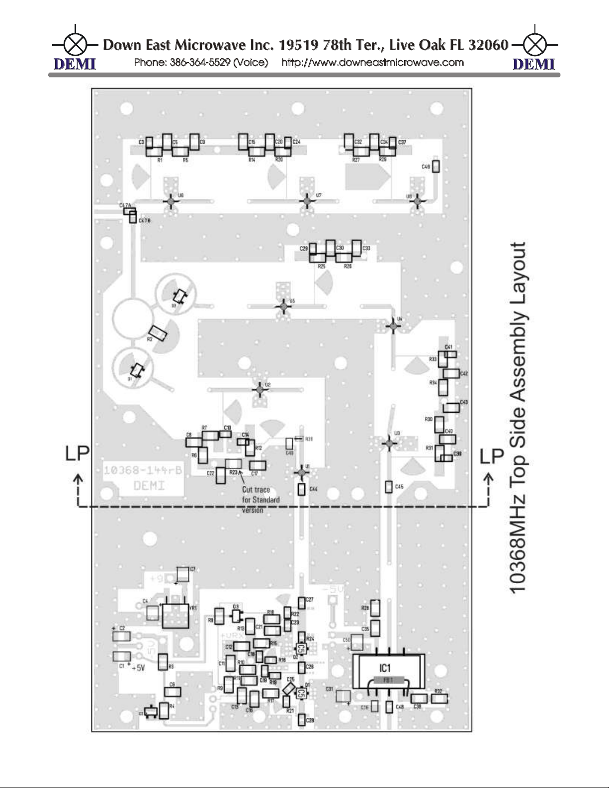
8. Referring to the component placement diagram, it depicts the standard version transverter
but the LP version is indicated on the placement. Use the component list to determine what
components are installed. For the actual assembly, start by installing the MMIC’s U1 - U8. You
will need a large solder iron to flow the solder on the ground leads. We use 40-watt irons with 700-
degree tips in the Factory. We also preheat the pallet to about 120 degrees F on a hot plate. You
may do the same with whatever means of pre-heating you have including the torch you used for
the pipe caps. If you can still handle the pallet after pre-heating, it could be hotter! The aluminum
pallet will hold the heat for a while but re-heating may be required, depending on your soldering
speed, to keep the solder flowing smooth. Be sure of the MMIC’s alignment. Consult the
component placement diagram with every installation. The MMIC’s are very difficult to remove if
installed incorrectly.
INPUT
FET N6 MMIC and MGA86576
U1 is different in the low power transverter. It will solder flat to the circuit in the Low power
(MGA86576) and the N6 in that position will be raised up in the HP unit. Be sure to install the
MMIC’s as flat and square to the pin alignment as possible [17]. U2-U8 may be installed the same
way centered above the holes in the board but he bodies of U2- U8 will fit squarely in the PCB
holes if flipped upside down. If you decide to do that, bend all four legs down before soldering. Be
sure to flow the solder on all of the ground leads up to the body of the MMICs. These leads need
to be a short as possible to ground. If you can see the ground lead, it’s not soldered correctly.
Use minimum amounts of solder on the input and output leads but solder them as close to the
body as possible.
After all of the 8 MMICs have been installed, use an Ohmmeter to check for shorts on the
input and output leads to ground. If you did a good job in prepping the PCB in step #2, you should
have no problems. If you do find a short, try wicking some of the solder from the shorted lead with
Solder Wick. If still shorted, try lifting the problem lead and re-wicking. Be careful not to break
the lead. A close inspection should reveal a short. Use the knife and re-move, then re solder and
re-test again.
If you have the HP version transverter, Install Q1, Q2 and VR1 paying attention to the
component document alignment. Use the same technique for Q1 and Q2 as U8 [18]. It is
important to get a good source lead to ground connection on the FET's and a ground connection

/Kits/10368-144CK_RevG.doc 6 Rev. G 5/9/2023
on the VR1 regulator so it may require some pallet heating. You could remove the mounting
screw near VR1 before soldering the ground tab.
8. Using the pictorial below as a guide for proper SMD soldering install all of the other surface
mount components in any order with the noted exceptions: [19]
Circuit board
Correct
Incorrect
Solder Fillet
Incorrect Component
Placement
Proper SMD Assembly.
Do not install R8, R18, D1 and D3
R38 is installed in the LP version and shorted in the standard version.
R23 is installed in the standard version only after cutting the trace for installation.
Verify the correct value for R12 depending on version of transverter.
It is easier to install all of the resistors in the low power section of the transverter first.
Install C47 in the "A" position.
You will need to remove the 4-40 screws to install C16 and VR1. Replace when soldered.
R3, R8 and R9 are just jumpers
If you have the HP version transverter, do not install IC1 and the jumper.
9. Install all of the filter probes (the silver pins) after cutting to the correct size [20].The length
indicated is the total length including the head. Cut 10 pins at 1/4” or 0.210 - 0.230”. Insert them
into F1- F3, F8 and F9, then solder [21] [22]. Cut the rest of the needed filter pins for F4 - F7
(there are extras!) to a total length of 3/16” or approximately 0.180” - 0.190” (F1 and F7 not
required for LP version). Insert pins in the remaining filter holes. Solder them in place using a
minimum amount of solder. You do not want the solder to “Icicle down” and extend the pin length
and thickness or short to the ground plane. Also, be sure that the pinhead is flat to the surface to
ensure that the probe is straight.
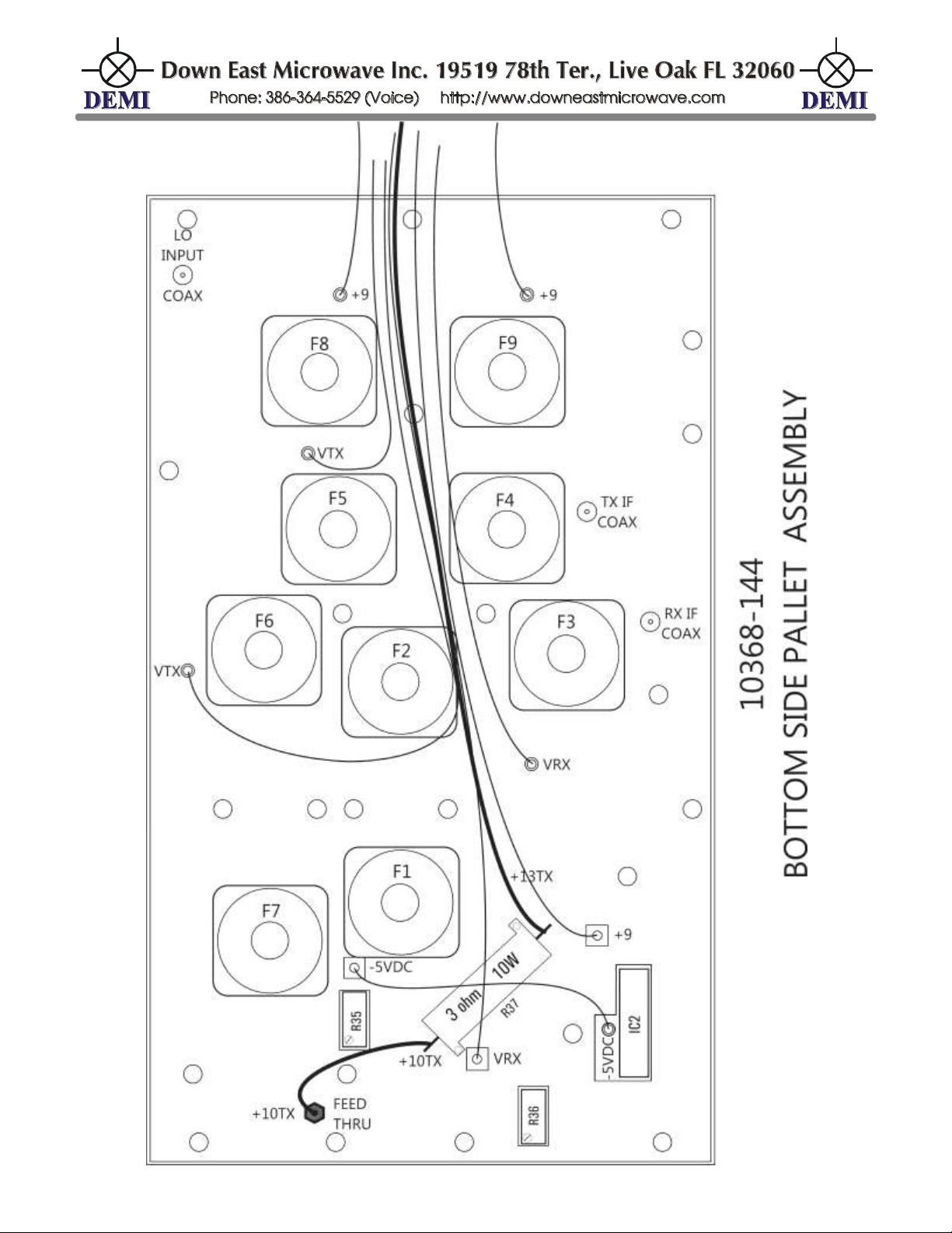
Install the 4-40 feed thru connector as shown on the bottom side pallet drawing (the filter
side off the pallet). The pin will come through the board near C31. Solder it to the pad and with an
ohm meter, verify it is not shorted to ground. Now, take the time to clean any excess flux off the
complete assembly with any cleaner you desire. It doesn't need to be "Spotless" just not coated
with excess flux.
10. With the clean pallet assembly, clear the foil in the mounting holes of IC1. Then, review the
FMM 5061LV pictorial for pin numbers and apply a very thin light of thermal compound to IC1
being careful not to smear any on the circuit board. Install with 3-48 screws. Be sure of the
alignment, tighten the screws and then solder the leads. The Copper foil will stretch enough and
conform to the installation. Now Fabricate the Ferrite bead jumper and install between both Drain
pins (4 and 6) keeping it as short as possible as shown on the component placement document
[23].
/Kits/10368-144CK_RevG.doc 7 Rev. G 5/9/2023
FMM 5061LV
11. Install the rear panel to the PCB by first prepping two SMA connectors so that the Teflon will
not interfere with the circuit board [24]. Insert the SMA connectors through the connector panel
and using the panel as a guide, trim the excess Teflon with a sharp knife flush with the panel.
Make a clean, square cut. Now trim the center pins to 1/16" extending from the Teflon. Attach the
SMA connectors to the panel with four of the #3-48 x 3/16” screws. Then attach the panel to the
pallet with five 3-48 x 3/8” screws. Look for any gaps or bulges between the pallet and the panel.
If so, remove panel and re-trim excess circuit board without cutting into the foil. Tighten the 5
screws evenly and be sure the cut center pins do not interfere with the circuit board. If needed,
dis-assemble and re-trim the Teflon on the connectors or the PCB and try again to obtain a perfect
fit. A complete flush connection of the pallet to the panel is the most important part of this kit.
TX
RX
PTT +13.8VDC AUX
GND
IF
PCB
Aluminum
Plate
Pipe Caps
10 MHz
Insert all of the 8-32 feed thru caps with a #8 ground lug on each by bending them in a right
angle for latter attachment. Then install two BNC connectors. Be sure to install the lock washer/
ground lug on the BNC connectors with the lugs positioned towards the RF connectors [25]. Then
Solder the SMA center pins.
12. All of the coax connections need to be made next. Start by cutting two 7” pieces (RXIF and
TXIF) and one 4" piece (LOIN). The best way of making this coax assembly will result in
something that looks like the next diagram. Start by removing approximately ¾” of the outside
jacket. Tin solder the entire exposed shield. Place the Rivet in position and solder in place. Try to
keep the coax in the center of the rivet while the solder cools. Now with a #22 wire stripper,
remove the shield that is below the rivet. The wire striper should score the shield if it is tinned and
you will be able to “Snap” off the shield. Then with a #28 wire striper, remove the insulation off the
center conductor. Leave a small amount of insulation as shown in the diagram below. Tightly wrap
the exposed center conductor and lightly tin the end. Be sure not to let the solder expand the
diameter of the center conductor and /or wick off [26].
3
2
16
5
4

/Kits/10368-144CK_RevG.doc 8 Rev. G 5/9/2023
1/4”
3/16”
1/16”
Insulation
Conductor
Prepped Coax details.
Once the coax is prepped, do a trial fit. Insert the center conductor through the hole in the
pallet and then through the hole in the PCB (either RXIF, TXIF or LOIN). The reason in making the
center conductor so long is so you have a guide for insertion. Fit the brass rivet into the pallet
hole. If it fits to tight (solder build up), scrape or file down the rivet’s high spot and try again.
Notice the tapped hole located close to the rim of the rivet. Insert a 4-40 x 3/16” screw and tighten.
The head of the screw should compress down on the rivet rim and hold it in place. Do not over
tighten [27].Then do the same for the other coaxes. After all coax is installed, cut off the excess
center conductor and solder it to the circuit. When complete install D1 and D2 on the RXIF and
TXIF. Be very careful with the lead alignment of the diodes.
13. On the HP version only as shown on the bottom side pallet drawing, install R35, R36 and
IC2 through the pallet into the board. Cut off excess leads. Then install the 3.3 ohm 10 Watt
resistor with two 3-48 x 3/16" screws. Now using the supplied #26 Teflon wire, cut, strip and tin the
ends of a 2.5" wires and connect it to both -5VDC points. All wires come in through the back of the
pallet through the 1/8” holes [28]. They are soldered to the circuit board where indicated on the
bottom side assembly diagram. They are the via holes with an "X". They can solder to any part of
the circuit board attached to the via.
The rest of the #26 wiring is labeled VRX, VTX, and +9 on both transverters.
Pass one end of the wire through the pallet in all of the indicated holes shown on the bottom
assembly document and solder. Cut, strip, and tin as before then insert one end of it through the
hole and solder to the board. After routing the wires as shown, cut them so they extend a
minimum of 3.5" past the end of the pallet.
Connect the +10TX connection from the feed thru to the10 watt resistor with a 1” #22 wire
and connect a 9” #22 wire to the other end of the 3.3 ohm resistor.
Wire the three rear panel feed through as follows. The center is connected to a 11" of #22,
the other two are connected to a 11" of #26. All wires should be routed as shown on the bottom
assembly [41].
14. Install all of the filter hardware now. The screw heights may be pre-set for tuning.
Examine the next pictorial. Set the 4-40 brass screws and stainless locking nuts to approximately
all the same height of 0.150”. The lock nuts should be "snug" but not locked.
Nut
0.150”

/Kits/10368-144CK_RevG.doc 9 Rev. G 5/9/2023
Re-inspect all solder connections. Touch up what is questionable. Now review the test
procedure before proceeding. Using the assembled unit for a “Dry Run” may clarify some of the
testing requirements that may have been in question when first read.
DC Testing:
1. With an Ohmmeter, check all resistors and wire connections for shorts or opens. Then
check the RXIF and TXIF cables for shorts. If all testing of the MMIC leads was a “Go” in
assembly step #8 the transverter is ready for DC and RF testing.
2. The MMICs, U1 –U8, if working correctly, will draw current. This current drain will cause a
voltage drop across the resistor network. With a +9 VDC supply, the total resistance in the bias
networks of all but the U8 MMIC (U1 in the low power Transverter) should be approximately 80 -
90 Ohms. With + 9VDC applied to the network the voltage drop should be approximately 5.3 volts.
This means U1 –U8 should have +3.5 - 4.0 VDC on the output lead and +2.5 VDC on the input
lead. The input lead voltage may vary up or down as much as 0.5 VDC or more. Apply +9VDC to
each stage in order and check the voltages on the leads of the MMICs. If large discrepancies
occur, check the bias resistors for correct value. If a MMIC does not draw current, it is dead (very
Rare!) or the resistor network is open. If it drops voltage down to less than 1 VDC, its leads are
shorted. Seek the problem out and repair. Now test in the following order: The LO stage, U6-U8,
the TX stage, U3–U5, and the RX stage to U1-U2 only. Do not apply voltage to the +VRX wire
attached to LNA section in the HP version
+9VDC
+2.5VDC
36
51
+3.5VDC
Input
DC Input
U4
Resistor Network with Voltage Points
U1 in the Low power transverter is different. The output lead should measure between +6
and +7 VDC. If it is over 7.2 VDC, remove bias immediately and check the bias resistors for
proper value. If the values are correct, R19 may need to be adjusted up in value. If it is less than
+5.5 VDC, the MMIC may be oscillating which could be caused by the filter not being tuned yet.
Place your finger on the input of the MMIC to verify if the voltage changes in an upward direction.
If the voltage measured is less than +2VDC on the output lead, it may have a solder short under
either lead. Check and repair.
3. If you have the HP version transverter, the LNA/PA section should be tested by verifying the
operation of IC2 first. Apply 9 VDC to the +9 and check for –5V (and it may be as low as –.7 VDC)

/Kits/10368-144CK_RevG.doc 10 Rev. G 5/9/2023
where indicated on the PCB. If OK, verify that the -5 V is on Pin 1 of IC1. If not adjust R35 to
obtain a maximum negative voltage. If -5 V cannot be obtained, examine the circuit for defects.
Check the LNA section by verifying a negative voltage on both Q1 and Q2 gates or inputs.
The voltage is limited by D2 and R4 and will not exceed -0.8VDC (or less than negative 1 volt) but
could be Zero volts. Adjust R36 so the both voltages are around -0.350 VDC. If it will not adjust,
seek the issue. It is either a short or open somewhere.
If OK, check the +5 V where indicated. It may be as high as +7.5 VDC. If OK install R8 and
R18 then connect +9VDC to the VRX wire that connects to R13 and R15. Measure the voltage at
the flag by R22 and adjust R36 to obtain between +2.0 and +2.2 VDC. Then verify approximately
the same on the flag by R19. Remove the VRX voltage when complete. The DC testing is
complete.
LO Testing:
The testing procedure will describe operation for 10368 MHz RF frequency with a 144 MHz
IF. It assumes the DIGILO will be used as the 3408 MHz oscillator. If a 145 MHz IF is desired,
select the correct DIGILO frequency. See its Chart. If anything other than a 2M IF frequency
range is desired, you may select any DIGILO frequency that will be multiplied by 3 to produce the
correct final LO frequency including an IF in the 70 cm band. Slight adjustment other than what is
detailed in this procedure may be required and RF test equipment such as a Spectrum Analyzer
may be required.
1. Connect a trimmed SMA connector to the 10224 TEST POIT. Be sure that it is a flush
mount [29].Verify that
C47 is in the test position
(C47A on the component
diagram). Install the
DIGILO as shown right by
installing two 4-40 x 1/4"
HEX standoffs and lock
washers in the pallet with
two 4-40 x 3/16" screws
for the board. Connect
the LO input to the RF
OUT of the DIGILO by
soldering the coax. Make
this coax connection as
short as possible [40].
The 10 MHz input is not
required for testing. Set
the correct jumpers (if not
done previously) by
shoring all 6 positions
except #4 for 10368 = 144
MHz. If you desire anything different, make the selections on the DIGILO now. Make the DC
connection to the DIGILO's +V with a 3" length of #26 wire [39].
2. Position the transverter so the LO Multiplier filter adjustment screws are easily accessible.
Connect a RF power-detecting device to the 10224 test point. It is preferred that this is a milliwatt

/Kits/10368-144CK_RevG.doc 11 Rev. G 5/9/2023
power meter but a diode detector may be used for peaking. Apply +9VDC to the DIGILO and the
two +9 wires on the transverter. If the screws are pre-adjusted correctly, some output power
should be detected. Adjust F9 first for maximum power. Use very slight adjustments (1/2 turn
maximum each way to find peak) while maintaining lock nut pressure to ensure the contact of the
screw to the pipe cap. Be careful of downward pressure with adjustment tools on the filter when
adjusting. Lock the nut into position when peak is found. Then adjust F8 for maximum power
using the same technique. Lock the nut when peaked. If using a detector diode you can only peak
it and on to step 2 of the RF test procedure. If using a milliWatt power meter, power should be
between + 3 and +10 dBm. Greater than is OK, less than is not. If test is OK, remove +9VDC and
go on to step 2. If the LO power is low, check the following in this order: Low DC Voltage, High
DC voltage (over +10VDC). Incorrect bias on U6 - U8, or C47 not in the test position "A". Low
level from DIGILO (coax short on either board). Also, revaluate the coax length between the
DIGILO and transverter. It is sensitive to length. As short as possible is required. If the LO power
is still below +3dBm, a snow flaking may be required in the coax input to the transverter. A simple
probing or touching will verify this. Add if required. Then consider the filters being tuned
incorrectly (wrong starting point). Incorrect probe length, probe missing, or probe shorted to
ground. Suspect defective MMIC last if voltages are correct. Always question your construction.
When test is complete, remove the SMA test connector and reposition C47 to the "B" position.
3. Further testing of
the transverter can be
completed to verify tune
up and operation. Both
the TXIF and the RX IF
cable can be temporally
connected to the BNC [43]
connectors and the tune
up procedure that is
described in the Testing:
may be followed except
the individual TXON and
RXON voltages are
applied as in the
DC Testing:section. For
the purest, this is the best
method to tune up the RX
section. This will allow the
ability to do any trimming
or snow flaking to optimize
the performance nut---
very little can be accomplished if the transverter is assembled correctly. But if you have a Noise
figure meter, the Gain and Noise Figure can be optimized. Connect the IF coax as show and test
and tune as specified in the test section. Then when complete, follow the next steps to complete
the assembly. If you decide to test and align the TX side, do not drive the TX mixer with more than
+10dBm.

/Kits/10368-144CK_RevG.doc 12 Rev. G 5/9/2023
4. For the complete testing of the transverter unit, the complete enclosure assembly should be
finished. Start by examining the two enclosure halves. Notice that in one half, there are four taped
holes. This is the transverter side. Install the microwave absorber in the bottom of the enclosure
as shown away from the end with the tapped holes [30].
Then unbolt the DIGILO and install the pallet assembly in the housing using the two 4-40 x 9/16”
screws and 1/8 spacers that are on the pallet. Remove the nuts and insert the pallet in the
enclosure being sure not to pinch any wires. Seat the pallet in place and start the screws. Now
start the two flat head panel screws (black in color). When everything lines up and you are sure
about the spacers being in place, tighten all four screws.
5. Install two 4-40 standoffs with split lock washers in the two remaining holes that are in the
transverter side of the enclosure. Make them snug but do not over tighten. The threads are
Aluminum. Now refer to the Installation section of the TC assembly document (pre assembled
earlier) and proceed with the installation. Be sure of your IF configuration and continue to the next
step below after completion [31].
6. If you are assembling the standard unit, the wire from the 3 ohm, 10-watt resistor should be
connected to the +13TX via on the TC board. Re-check all connections and verify that there are
no lose wires, if so identify and connect if needed. Check all mounting hardware and connectors
to be sure nothing is lose.
Testing:
1. Start by getting the same equipment ready that was used for the LO testing. Preset the IF
pots on the TC board by turning the TXIF counter clockwise and the RXIF clockwise. Connect
13.8VDC to the transverter and switch the power on. The green LED should light. If you connect
an external 10 MHz source, the Loc light should change to Green. If not it should be Red [32].
Check voltages on the TC board. There should be +9VDC on the VRX and the +9 points. There
should also be +13.8VDC where indicated on the TC. Now toggle the TC board by activating the
PTT circuit. The relay will click and the TX LED will light. VRX drops to zero volts and the VTX will
now be +9VDC and the +13TX will measure the transverter's input voltage.
2. Even though the fixed attenuator has been predetermined, for initial testing, the TXIF pot
should be adjusted to the maximum attenuation position (full counter clockwise). If you don’t,
excessive drive may produce spurious signals and make aligning the TX chain more difficult.
Connect a RF power detector to the TXRF port of the transverter after verifying the correct
attenuation for the version of transverter you have. Position the transverter so the filter
adjustments are accessible [33]. Key the PTT circuit and apply the 144 MHz TX signal to the
transverter. If the adjustment screws of the filters were pre-set, monitor the power detector and
adjust F4, F5, F6 and F7 if you have the standard version in order. Start by turning them IN, 1/8 of
a turn at a time maintaining lock nut pressure. Power should be detected eventually. When power
is detected, remove the 144 MHz IF signal to verify that the detected signal vanishes. You may
also want to adjust the TXIF pot on the TC board to verify operation. If the power doesn’t change,
you have tuned the filters to the LO frequency. If so, continue adjusting the screws 1/8 turn at a
time in the same IN direction until the next power peak is detected. Verify that it is the desired
signal by removing the 144 MHz IF signal. When you are sure you have the desired signal, peak

/Kits/10368-144CK_RevG.doc 13 Rev. G 5/9/2023
all filters one at a time starting with F5. After each filter is peaked, remove the 144 MHz IF signal
and re-verify that the detected signal vanishes. Final output power should be the limit of the
version transverter you have at the desired IF drive level. Toggle the PTT with the IF drive off and
check for oscillations. If none are detected, proceed to the RX testing.
If output power is less than specified, check the following in this order: Low or High voltage.
Verify that the DIGILO is connected to +9VDC. Check C47 to verify it is installed in the "B" position
(need to remove pallet to check this). IF drive power level either too low or too high or wrong
configuration on the TC. Is the IF coax cable short or open? Is C45 (LP) or C48 (standard)
damaged from the connector installation? Filter Probes (length, shorted, missing?). D3 blown
from excessive drive. Suspect defective MMIC last if their voltage is correct. Always Question
Construction! AND the 3 watt MMIC is never bad unless installed backwards!!
3. To test the 10368 RX, a signal source at the desired receive frequency is required. This
may be a signal generator, a harmonic from a transmitted signal source, or a on the air signal
transmitted from a 10.368 GHz transmitter. The IF port should be connected to a 144 MHz
receiver with an “S” meter, though a low level power meter, spectrum analyzer, noise figure meter
or service monitor may be used. The transmitted signal from the transverter should not be used
because of the use of the same IF frequency. It would be very difficult to determine what was the
desired signal versus the radiated 144 MHz signal being detected in the IF receiver, no matter
what level it was. At the factory, a 10368 MHz signal generator set for -30 dBm for the LP and
–50dBm for the standard version and is injected directly into the RXRF port of the transverter then
adjusted for maximum gain into a 144 MHz receiver. Then we test and optimize it with a noise
figure meter [34].
Your actual testing and alignment starts with generating a 10368 MHz signal and detecting
it on a 144 MHz receiver through the RXIF connector on the transverter. Be sure that the 10368
RX port is terminated with a 50 ohm device while adjusting the filters. If connecting a signal
generator directly to the RX port, do not exceed -30 dBm. A signal source higher than that will
compress all of the gain stages, possibly generate harmonics, and make alignment difficult. With
the DC power applied to the transverter, adjust F2 and F3 filters (and F1 if you have the standard
transverter) by turning the screws IN to maximize the IF level signal strength. Adjust 1/8 of a turn
at a time while maintaining lock nut pressure. Keep adjusting until peaked. When complete, lock
the nuts. The LNA bias adjustment should not be adjusted unless you are testing the transverter
with a noise figure meter and then in conjunction with additional filter tuning.
If RX gain is less than expected, check the following in this order: Low or High voltage.
Verify if the RXIF gain control is at minimum or the RXIF gain stage on the TC board, if installed, is
working correctly. Verify the input signal level. If it is too high, it could cause harmonics in the
Q1/Q2 stage allowing the misalignment of the filters. Is Q1/Q2 oscillating? Is the IF coax cable
short or open? Is C44 (LP) or C28 (standard) damaged from the connector installation? Filter
Probes (length, shorted, missing?) Is D1 blown from excessive drive during the TX test while not
keying the PTT line? This would also cause damage to the RXIF Gain stage but suspect defective
MMIC on the Transverter board last if the voltages are correct. Always Question Construction!
Completion:
When you become satisfied with the RF operation of the 10368-144, you need to install the
External 10 MHz. coax to the DIGILO and wire it's LOC detect line to the "IN" via on the TC board
located next to the ON/OFF switch. Then test by connecting a external 10 MHz source and verify
that the LOC led changes from RED to GREEN.
Now, you may want to bundle all of the control wires and coaxes together to make a neat
appearance (see next picture) [35]. It is not necessary, but it will contain the wires to make closing
/Kits/10368-144CK_RevG.doc 14 Rev. G 5/9/2023
the enclosure easier. Do a final check on the TX and RX IF levels and if you are satisfied, close
the enclosure and bolt it with the four remaining flat-head screws. Be sure not to pinch any wires
or coax and re-test the transverter after closing.
This completes the assembly and testing of the 10368-144. You now have enough
knowledge of how this assembly works that implementing it into a complete working system should
not be a technical problem. Remember that the unit is designed to operate from a +13.8VDC
source but any voltage between 11 and 16.5 VDC will work making it perfect for portable
operation. You may wish to test this before going portable.
The LP versions receive conversion gain is limited and may require some additional
amplification. To overcome your IF switching scheme insertion loss when interfacing the
transverter with a 144 MHz transceiver, you may want to install the MMIC in the TC board. If the
transverter is to be used in a high performance terrestrial or EME set up, a Low Noise Amplifier
should be considered [36]. If so, additional filtering and isolation may be required and/ or the use
of the RX OPT may need to be omitted. If a higher power amplifier is added, consider a additional
filter and/or isolator [37]. Also consider some attenuation if using a high gain TWT amplifier for +5
dBm may be too much driving power.
The standard version only needs a SMA TR switch to make it a top-notch portable rig mated
to a modest size antenna that will produce Hill top DX! Both units can be interfaced with any 2M
transceiver in its standard form if it doesn't exceed 10 watts. Higher output power transceivers are
not recommended unless modified or adjusted to prevent damage. Addition of external power
amplifiers and LNA’s can be accomplished with the AUX output of the transverter or by
implementing a sequencing scheme. Remote location mounting is possible with this unit in its
stock form. It would just need to be installed in a weatherproof enclosure.
Conclusion:
We hope you had fun with this kit and that you enjoy many hours of operation with your
completed transverter. Please take time to read the papers published by W1GHZ (N1BWT) for
other operation tips and suggestions including antenna designs and a similar 5760 MHz
transverter design. Good luck with the DX and have fun!
NOTICE:
This equipment is to be used solely by licensed amateur radio operators within the
specifications and guidelines governed by their licensed agreements.
/Kits/10368-144CK_RevG.doc 15 Rev. G 5/9/2023
This product should not be thrown away. Please dispose any components or equipment
properly. By reusing, returning or using proper collection points which are designated for it.
10368-144LP Transverter Board Parts List
All components are Surface Mount. All resistors are 1206 size unless indicated. All capacitors are
1206 size except for 1.0pF are 55mil ATC. All others are as indicted. Any substation of values or
types is at users own risk.
C3 1.0 pF
C29 1.0 pF
C44 1.0 pF
R12 51 or 100(LP)
R34 36
C5 0.1F
C30 0.1F
C45 1.0 pF
R14 36
R 35 100
C8 0.1F
C32 100 pF
C46 5 pF (0805)
R20 51
R38 short or 51(LP) (0805)
C9 1000 pF
C33 100 pF
C47 1.0 pF
R23 36Not in LP
U1 N6 or MGA86576 (LP)
C10 1.0 pF
C34 0.1F
D1 HSMS8202
R25 51
U2 N6
C14 1.0 pF
C37 1.0 pF
D3 HSMS8202
R26 36
U3 N6
C15 100 pF
C39 1.0 pF
R1 51
R27 75
U4 N6
C17 0.1F
C40 0.1F
R2 51 (0805)
R29 51
U5 N6
C20 0.1F
C41 1.0 pF
R5 36
R30 36
U6 N6
C22 100 pF
C42 0.1F
R6 36
R31 51
U7 N6
C24 1.0 pF
C43 100 pF
R7 51
R33 51
U8 N6
10368-144 3 watt version additions.
All chip resistors are 1206 size unless indicated. All 1.0pF capacitors are ATC 55mil. 4.7F is a
tantalum and the white band indicates positive polarity. Any substation of values or types is at
users own risk.
C1 4.7F
C21 100pF(0805)
C49 0.1F (0805)
R8 0
R22 51(0805)
C2 4.7F
C23 0.1F (0805)
C50 4.7F
R9 0
R24 15(0603)
C4 4.7F
C25 0.1F (0805)
D2 MMBD914
R10 470
R28 51(0805)
C6 0.1F(0805)
C26 1.0 pF
FB1 Ferrite Bead
R11 240
R32 51(0805)
C7 4.7F
C27 1.0 pF
IC1 FMM5061VF
R13 5.1K
R35 200Pot
C11 100pF(0805)
C28 1.0 pF
IC2 NMA0505S
R15 5.1K
R36 1KPot
C12 100pF(0805)
C31 4.7F
Q1 CE3512K2
R16 51(0805)
R37 3, 10 W
C13 100pF(0805)
C35 0.1F (0805)
Q2 CE3512K2
R17 470
VR1 78M05
C16 100pF(0805)
C36 1.0 pF
Q3 MMBT3904
R18 220
C18 0.1F (0805)
C38 0.1F (0805)
R3 0
R19 51(0805)
C19 0.1F (0805)
C48 1.0 pF
R4 5.1K
R21 51(0805)
10368-144LP board and enclosure hardware Parts List
7 1/2” Pipe Cap
8 4-40 locknuts
20 silver pins
1 machined 1/4” plate
22 4-40 x 3/16
5 3-48 x 3/8”
3’ RG-188 coax
3 SMA connector
6 3-48 x 3/16”
8 4-40 x 3/8” brass
3’ # 28 Teflon wire
2 BNC connector
2 4-40 x 3/8”
1 # 4 Ground Lug
1 SPDT switch
2 Machined End Plates
2 4-40 x 9/16
4- #4 split washers
3 8-32 feed thru
8 Flat head screws
3 4-40 x 1/4”
2- #4 x 1/8” spacer
4 1/8” x 3/16” rivets
1 Hole plug
2 4-40 nuts
41/4” threaded standoff
LNA and Power Amplifier Section Hardware
/Kits/10368-144CK_RevG.doc 16 Rev. G 5/9/2023
4- 3-48 x 3/16”
2- 4-40 lock nuts
4- silver pins
2- 4-40 x 3/8” Brass
2 - 1/2” Pipe caps
8- 4-40 x 3/16
24” #22 Teflon wire
1- 4-40 feed-thru
C45
C39 C40 C43
R31 R30
U3
F6
U4
F5
U5
F4
C29 C30 C33
R25 R26
C41 C42
R33 R34
D3
D1
R2
F3
U2
F2
U1 C44
R38
(Add for Standard
Version)
R23
R7
R6
C8 C10
C22 C17 C14
C47A/B U6
F9
U7
F8
U8
C3
R1 R5 R14 R20 R27 R29
C5 C9 C15 C20 C24 C32 C34 C37
C46
LO IN
10224MHz TP
+9
VRX
RX IN
RX IF
TX IF
VTX
VTX
TX OUT
10368-144LPrC TRANSVERTER SCHEMATIC
(Short for Standard Version
51ohm (0805) for LP Version)
R12
C49

/Kits/10368-144CK_RevG.doc 17 Rev. G 5/9/2023

/Kits/10368-144CK_RevG.doc 18 Rev. G 5/9/2023
/Kits/10368-144CK_RevG.doc 19 Rev. G 5/9/2023
/Kits/10368-144CK_RevG.doc 20 Rev. G 5/9/2023
This manual suits for next models
1
Other demi Media Converter manuals


Popular Media Converter manuals by other brands


Crestron
Crestron DigitalMedia DM-NVX-350C quick start guide

Coltene
Coltene BioSonic S1 owner's guide

TR-Electronic
TR-Electronic Profibus 582 Series Assembly instructions

Baumer
Baumer HOG 9 Mounting and operating instructions

Altronix
Altronix NetWaySP8A installation guide

Sony
Sony BKSI-2020 installation manual