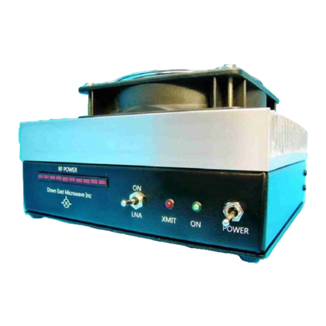
demi 1296-144 K User manual

/Kits/1296-144CK.doc 1 8/15/2011
DEM Part Number 1296-144 PCB, K and CK
23 cm Transverter PCB, Board Kit, and Complete Kit
Specifications
Frequency range:
1296 MHz. = 144 MHz.
Noise Figure and Gain:
<1.5 dB NF, > 17 dB Gain with >+5dBm IP3 Input
Power Output:
3 watts. Lower levels with different configurations
TXIF Drive level:
1 mW to 10 Watts maximum dependant on IF configuration.
DC Power requirements:
13.8 VDC nominal. 11 to 16.5 VDC operational.
DC Current drain:
500 mA to 2.5 Amps depending on output power level.
Operational Overview
The DEM 1296-144 is a 23 cm to 144 MHz transmit and receive converter. It has a linear
output power of approximately 3 watts and may be achieved with as little as 10 mW or a maximum
of 10 W of IF drive with the correct IF configuration. The highlight of this transverter is the receive
section. The design uses a PHEMT that has a high-pass tuned input circuit biased for High IP3
output performance. It is followed by two 3 pole helical filters, a high output IP3 MMIC gain stage,
and a high level mixer with a IP3 output of +30 dBm. This design provides a sensitive low noise
receiver with superior out of band signal rejection that will tolerate IP3 input signals > +5 dBm!
Other improvements over the previous versions of 1296 transverters are in the Local Oscillator
and TX section. The base oscillator of the local oscillator circuit is housed in a shielded enclosure
on the circuit board. This shield coupled with the higher frequency base oscillator operation, (192
MHz), reduces the amount of spurious output while providing greater temperature stability. The
transmit section has improved filtering to eliminate all other spurious emissions. The DEM 1296-
144 has a built in transmit / receive relay on the RF side with provisions for external switching for
adding a high power amplifier or preamplifier to your 23 cm system. The 144 MHz IF levels and
options are adjustable on both transmit and receive with a dynamic range of approx. 25 dB. This
is useful for adjusting your maximum output power and setting the "S" meter level on your IF
receiver. The IF connections are via BNC connectors. Options have been provided for a key line
input PTT-H (+1 to 15 VDC) or PTT-L (a closure to ground) and auxiliary contacts on either
transmit or receive with a common line for many applications. The control, power, and auxiliary
connections are via RCA jacks. The 23 cm connectors are Type 'N' or SMA if separate TX and RX
ports are chosen. The 1296-144 is housed in our standard 4.125" x 1.875" x 7.75" extruded
aluminum enclosure that matches all of our other microwave transverters.
General Information
The detailed technical design information is posted in the library section of the Down East
Microwave Web site. The paper stresses the receiver’s immunity to out of band signals and
covers the design stage by stage. The 1296-144 kits and PCB are supplied with a schematic and
component placement diagram. The PCB is made of 0.062” thick Fiberglass G10 material. It has
plated 1 oz. copper with plated through ground Vias and will only require a general understanding
of the circuit design accompanied by good construction practices to produce a great working
transverter. The circuit board alone may be assembled and used in many different configurations.
It is perfect for the experimenter in the 23 cm band and requires very little microwave expertise.
The PCB by itself doesn’t require external mechanical support but will require a special
mounting technique. Down East Microwave will guaranty the performance of our circuit board
with your configuration but will not repair any transverters built from the 1296-144PCB unless

/Kits/1296-144CK.doc 2 8/15/2011
all components used are specified on thecomponent list that accompanies the PCB when
purchased!
For a higher probability of success, and 100% support of Down East Microwave Inc., we
recommend at the minimum, using the 1296-144K. The K (kit version) includes the PCB and all
components required to produce a low transmit level 23 cm transverter. If higher output power is
required, you may simply order the hybrid power module that the circuit was designed for but
physical mounting may be difficult due to components located on both sides of the circuit board.
For this reason, if you wish a 3 Watt unit, we recommend using the complete kit version. The
1296-144CK (complete kit) includes the board kit and the hybrid power module along with all the
necessary hardware, connectors and enclosure. Also included in the CK is a special mounting
plate that allows the mounting of the assembled PCB and hybrid module into the enclosure
provided. The circuit board mounting plate is machined so that the helical filters, PCB, local
oscillator shield, the hybrid power module, and all external DC and RF connectors are mounted
together as a complete assembly before installing in to the enclosure. This plate is the key to the
maximum reliability of the transverter (heat transfer and spurious oscillations) and allows complete
alignment before final assembly into the enclosure.
Circuit Description
A local oscillator of 192.00 MHz is multiplied X 6, filtered, and amplified to the +17 dBm
level then is injected into a high level mixer. In receive, the 23 cm signal enters through either the
RX port or the common antenna port. It is amplified by a high level, tuned input PHEMT low noise
amplifier that has approximately 16-17 dB of gain with <1.0 dB noise figure. The input circuit is
designed to attenuate all signals out side of the desired 23 CM band. The amplified signal then
passes through a 3 pole helical filter that allows approximately 30 MHz. of amplified bandwidth.
This signal is then amplified by a high level MMIC before being filtered by the next 3 pole helical
filter that restricts the receivers operation to a narrow segment of the 23 CM amateur band. This
signal enters the high level mixer and exits the IF port passing through a VHF low pass filter and
optional IF gain stage with a variable attenuator. Then depending on the configuration, it will pass
through the IF switch or not before becoming available to the 28 MHz. receiver.
On transmit, it is a reverse process. The 2 meter transceiver applies a signal of up to 10
watts of drive and it is then attenuated and filtered before entering into the mixer. The 23 cm
transmit signal then exits the mixer and is filtered by the 3 pole helical before being passed
through the transmit gain stages. It is then amplified up to approximately +15 dBm before it is
filtered again to narrow the pass band energy. At this point the signal can be used as is or be
amplified up to the 3 watt level before either exiting the TX port or the common antenna port.
Other LO input, RF and IF frequency schemes may be used with the 1296 transverter such
as our other 28 MHz IF versions or the 1268/9 transmit converters. Simply do the math. There
are a few limiting factors for different frequencies of operation. The IF will operate on any
frequency between 28 and 188 MHz. With the correct LO filters. The RF filters will cover the whole
23 cm band. The LO filters in this kit will not tune to a 28 MHz IF range. All filters included in the
kit may need to be re-tuned or replaced and the levels will need to be checked. Therefore, if
attempting a large frequency change or using an odd IF frequency, is not recommended unless
you have a known signal source and a spectrum analyzer to determine your desired outcome of
the transverter.
For a more detailed circuit description about any component or circuit in particular, or if you
have questions about a desired scheme, we recommend you contact Down East Microwave
before proceeding with a modification to the kit.

/Kits/1296-144CK.doc 3 8/15/2011
Assembly Tips
It is recommended to read the entire document before you begin to assemble the kit, but
the following few paragraphs is a compilation of assembly techniques used and required to
assemble this kit. These various assemble techniques will be used for more than one component
and may determine the outcome of this kit. Review the examples shown and become familiar with
the components described in the text.
Soldering surface mounted active components
The dots or angle cut leads on the MMICs IC1-IC3, IC5-IC7 are as shown on the
component placement diagram and determine their correct orientation. IC10 is a 3 leaded package
with a solder tab. Its orientation is shown on the component placement diagram. The MMIC’s must
be positioned correctly prior to soldering. Removing a MMIC without damage is difficult. The
PHEMT Q3 has a wide lead for one of the source leads. (See figure 1B) Leads on all active
surface mounted components should be somewhat flat against the mounting surface, if they are
not, a small tool such as a small bladed screw driver can be used to flatten them before attempting
to solder (See Figure 2). After verifying that the leads are flat to the surface, you will be ready to
solder.
1. To begin to solder, pick one pad on the circuit board that you wish to attach the active
device to. Without the component in place, heat one side of the mounting area and Tin the area by
flowing a small amount of solder on it. Allow it to cool.
2. Align the desired component on the circuit board based on the placement diagram. While
holding the component in place, apply heat to the tinned pad and re-flow the existing solder until
the component lead “drops” into the solder. Allow to cool and observe the alignment of all of the
leads.
3. If the alignment is acceptable, solder the remaining leads. You need enough solder to
cover the lead and mounting surface of the entire lead length. (See Figure 2 shaded areas) If
necessary, re-solder the original lead.
03
Input Lead is
angle cut
S
D
G
S
ATF34143
Figure 1A Figure 1B
PCB Trace
Leads flat to trace, 4 places
Some spring back is OK
Solder shown in shaded areas
Solder full length of lead, 4 places
Typical side view of four leaded surface mounted device, lead bending close to body.
Figure 2

/Kits/1296-144CK.doc 4 8/15/2011
Soldering surface mounted passive components such as chip resistors and capacitors:
1. Determine the component mounting position based on the assembly diagram.
2. Without the component, tin one of the mounting pads not shared by another component.
(Flow a small amount of solder on it)
3. After cooling, place the component in the correct position per the assembly diagram, it
should now have one end over the tinned area.
4. Holding the component in place with tweezers or other soldering aid, heat the tinned area
and allow the solder to flow around the component. Remove the heat.
5. Once solidified, remove holding tool and heat and flow solder to the other side of the
component only if it is not shared by a second component. If so, solder the component that
shares the pad first. You are done! See examples in figure 3.
Circuit board
Correct
Incorrect
Solder Fillet
Incorrect Component
Placement
Figure 3. Proper SMD Assembly.
Soldering leaded components (resistors, capacitors, diodes, and inductors) :
Depending on your available tools, you can solder your transverter's leaded components
from either the top or bottom of the PCB. It is suggested for the home assembler to use a method
that is comfortable. A simple holding vise can be utilized to allow the components to be 'dropped
in' from the top side and soldered on this side without flipping over the assembly. As an alternate
method, you can insert one component at a time in the correct mounting location and gently push
down to the circuit board, while holding the component, flip over the circuit board and bend the
leads over in opposite direction to hold the component in place. Although this is the most reliable
method, there are some drawbacks if the component must be removed when the PCB is installed
in the enclosure.
Some leaded components may need to be surfaced mounted either on one or more leads.
If this is the case, the leads need to be pre-formed before soldering. If you see a leaded
component on the component placement diagram without a circle at the end of the lead such as
R25 and C49, those leads will need to be surfaced mounted as shown in the drawings below. DO
NOT install any leaded components in the ground via holes if it is shown as a surface mount lead.
The PCB mounts to a pallet and if there is any solder or extended lead interference, the PCB will
not be flush with the pallet.
Leads soldered to PCB surface
Circuit Board Surface
This end soldered to PCB surface
Circuit Board Surface
Figure 4
.
Some inductors are pre-formed and some will need to be formed such as L1. It is
suggested that the coils be formed on the supplied wooden dowel. Winding coils is not an exact
science and you should not be intimidated by it. Using the enamel wire supplied, extend about ¼"
in a perpendicular direction off of the dowel and wind the wire around it, counting each revolution
as one turn. When the total number of turns is completed (see the component list) cut the wire an
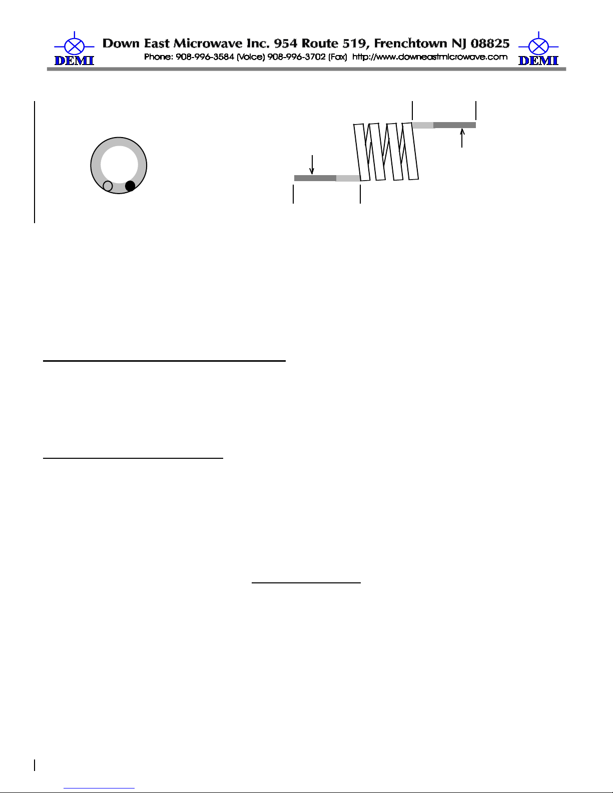
/Kits/1296-144CK.doc 5 8/15/2011
additional ¼" beyond the dowel. Form the two ¼" leads so they are pointing in the direction as
shown in Figure 5.
End view of formed coil
Top view of normally formed coil, (4 turns shown)
1/4"
1/4"
Solder Tinned Area
Solder Tinned Area
Figure 5.
Dress the turns together if they are out of shape from winding, remove the coil from the
dowel. The coil forming is complete! To ensure a positive solder connection, the ¼" leads should
be solder tinned as follows. With a solder iron, flow a pool of solder on the tip. Place the desired
end of enamel wire in the pool of solder. It may take a few seconds depending on the iron
temperature, but the red enamel will melt and be replaced with a solder tinning. Also tin L5. It is
pre-wound.
Rework of soldered components if needed
The easiest method to rework soldered components is to employ a de-soldering braid that
is specifically designed for this purpose. It can be purchased at most electronics component
distributors. Place the de-soldering braid on the lead that you are removing and apply heat to it.
Without excessive pressure the solder will flow into the braid leaving the lead or component
ready to be removed.
Printed Circuit Assembly Notes
Your kit is provided with easy to read component placement diagram that details every
components placement and the reference designators that correspond to the provided component
list (Bag 1 - Bag 4). Each side of the printed circuit board (PCB) is also shown to eliminate mirror
image assembly errors. The top and bottom side assembly operation should always begin by
aligning the PCB outline with the out line of the component placement diagrams. The top side of
the circuit board is the side with the printed lettering on it. Most of the soldering will be done on the
top side. Again, when soldering on the ground plane, be sure that solder does not flow and pool on
the bottom side of the PCB.
Start the Assembly
This is a basic assembly instruction document. Every filter has been installed and tested in
the circuit board. Adjustment should not be required. As of now, this kit is for a average to
experienced RF circuit builder. To align this kit, it will only require a volt meter, a 23 CM signal,
and a power meter that will measure up to 5 watts maximum. If you have access a frequency
counter, a signal generator, and a mW power meter it would be a plus. Please note that this
document assumes the Complete Kit. If you have purchased the 1296-144K, only use construction
details that pertain to the circuit board.
Inventory the parts list. Every part in this kit is important and should be identified. Bag 1
contains resistors, Bag 2 contains capacitors, Bag 3 are the inductors and Bag 4 are the
semiconductors and relays. The filters are listed on the components list but are installed. Take
your time to get familiar with the kit contents and verify it is complete. There are extra chip
components packed in the vials, so no need to count them. Just verify that the value is included.
This manual suits for next models
2
Other demi Media Converter manuals
Popular Media Converter manuals by other brands
H&B
H&B TX-100 Installation and instruction manual

Bolin Technology
Bolin Technology D Series user manual
IFM Electronic
IFM Electronic Efector 400 RN30 Series Device manual

GRASS VALLEY
GRASS VALLEY KUDOSPRO ULC2000 user manual

Linear Technology
Linear Technology DC1523A Demo Manual
Lika
Lika ROTAPULS I28 Series quick start guide
Weidmuller
Weidmuller IE-MC-VL Series Hardware installation guide
Optical Systems Design
Optical Systems Design OSD2139 Series Operator's manual

Tema Telecomunicazioni
Tema Telecomunicazioni AD615/S product manual
KTI Networks
KTI Networks KGC-352 Series installation guide

Gira
Gira 0588 Series operating instructions
Lika
Lika SFA-5000-FD user guide
