Densei-Lambda ZWS150PAF Series User manual


- 2 -
DENSEI-LAMBDA
ZWS150PAF Series
INSTRUCTION MANUAL
1-2. ZWS150PAF/J
1 L: AC Input terminal (pin 1 of CN1)
Live line (fuse in line)
2 N: AC input terminal (pin 3 of CN1)
Neutral line
3 FG: Input terminal FG (pin 5 of CN1)
Safety earth (Frame Ground)
Connect to safety ground of apparatus
or equipment.
4 FG: Frame Ground (Connected to pin 5
of CN1)
Must be connected to electrically safety
ground of apparatus or equipment by
electrically conductive spacers. The
mounting surface of the spacer should be
within MAX 8mm.
5 CN2: ON/OFF control terminal (primary circuit)
See NOTE A
6 +: +Output terminal
7 - : - Output terminal
8 V.ADJ: Output voltage adjust trimmer (VR51)
The output voltage rises when a trimmer is
turned clockwise.
9 CN52: ON/OFF control terminal (secondary circuit)
(For power supply output on and off control
with an external signal.)
*Input & Output connector ( J.S.T )
(also for option model /JL,/JA)
Connector Housing Terminal Pin
Input (CN1) B3P-5-VH VHR-5N SVH-21T-P1.1
Output (CN51) B6P-VH VHR-6N SVH-21T-P1.1
*Output Current of each connector pin must be less than 5A.
*Hand Crimping Tool : YC-160R ( J.S.T )
*CN2 is normally shorted by JM-2W-96 ( J.S.T )
See NOTE A
Connector Housing Terminal Pin
B2B - XH - AM XHP - 2 BXH - 001T - P0.6
or SXH - 001T - P0.6
N
OTE A: For COVER & CHASSIS type (MODEL: ZWS150PAF/JA), remote ON/OFF control cannot be used.
*Connector for Remote ON/OFF control: CN2
,
CN52
*Hand Crimping Tool: YC-110R (J.S.T) or YRS-110 (J.S.T)
(J.S.T)

- 3 -
DENSEI-LAMBDA
ZWS150PAF Series
INSTRUCTION MANUAL
1-3. ZWS150PAF/T
1 L: AC Input terminal L (M4 screw)
Live line (fuse in line)
2 N: AC input terminal N (M4 screw)
Neutral line
3 FG: Input terminal FG (M4 screw)
Safety earth (Frame Ground)
Connect to safety ground of apparatus
or equipment.
4 FG: Frame Ground
Must be connected to electrically safety
ground of apparatus or equipment by
electrically conductive spacers. The
mounting surface of the spacer should be
within MAX 8mm.
5 CN2: ON/OFF control terminal (primary circuit)
See NOTE A
6 +: +Output terminal (M4 screw)
7 - : - Output terminal (M4 screw)
8 V.ADJ: Output voltage adjust trimmer (VR51)
The output voltage rises when a trimmer is
turned clockwise.
9 CN52: ON/OFF control terminal (secondary circuit)
(For power supply output on and off control
with an external signal.)
See NOTE A
* Input & Output connector ( EMUDEN )
(also for option model /TL,/TA)
*CN2 is normally shorted by JM-2W-96 ( J.S.T )
Connector
Input (CN1) T6957-A
Output (CN51) T7094-A
Connector Housing Terminal Pin
B2B - XH - AM XHP - 2 BXH - 001T - P0.6
or SXH - 001T - P0.6
N
OTE A: For COVER & CHASSIS type (MODEL: ZWS150PAF/TA), remote ON/OFF control cannot be used.
*Hand Crimping Tool: YC-110R (J.S.T) or YRS-110 (J.S.T)
*Connector for Remote ON/OFF control: CN2
,
CN52(J.S.T)

- 4 -
DENSEI-LAMBDA
ZWS150PAF Series
INSTRUCTION MANUAL
1-4. ZWS150PAF/S
1 L: AC Input terminal L (M4 screw)
Live line (fuse in line)
2 N: AC input terminal N (M4 screw)
Neutral line
3 FG: Input terminal FG (M4 screw)
Safety earth (Frame Ground)
Connect to safety ground of apparatus
or equipment.
4 FG: Frame Ground
Must be connected to electrically safety
ground of apparatus or equipment by
electrically conductive spacers. The
mounting surface of the spacer should be
within MAX 8mm.
5 CN2: ON/OFF control terminal (primary circuit)
See NOTE A
6 +: +Output terminal (M4 screw)
7 - : - Output terminal (M4 screw)
8 V.ADJ: Output voltage adjust trimmer (VR51)
The output voltage rises when a trimmer is
turned clockwise.
9 CN52: ON/OFF control terminal (secondary circuit)
(For power supply output on and off control
with an external signal.)
See NOTE A
*Input & Output connector ( EMUDEN )
(also for option model /SL,/SA)
*CN2 is normally shorted by JM-2W-96 ( J.S.T )
Connector
Input (CN1) T6969-A
Output (CN51) T7093-A
Connector Housing Terminal Pin
B2B - XH - AM XHP - 2 BXH - 001T - P0.6
or SXH - 001T - P0.6
N
OTE A: For COVER & CHASSIS type (MODEL: ZWS150PAF/SA), remote ON/OFF control cannot be used.
*Hand Crimping Tool: YC-110R (J.S.T) or YRS-110 (J.S.T)
*Connector for Remote ON/OFF control: CN2
,
CN52(J.S.T)

- 5 -
DENSEI-LAMBDA
ZWS150PAF Series
INSTRUCTION MANUAL
2. Terminal Connecting Method
Pay attention to the input wiring. If it is connected to
wrong terminal, the power supply will be damaged.
• Input must be off when making connections.
• Connect FG terminal of input connector and mount-
able FG to ground terminal of the equipment.
• Output current of each connector pin must be less
than 5A. ( Except /T, /S models which M4 screw is
used. )
• The output load line and input line shall be separated
and twisted to improve noise sensitivity.
• Remote ON/OFF control lines shall be twisted or use
shielded wire.
• Use the input/output connector housing, terminal pin
as specified in outline drawing. Also, use recom-
mended crimping tool.
Connector housing and terminal pin is not included
with this product.
• When connecting or removing connector, do not ap-
ply stress to PCB.
ZWS150PAF
ZWS150PAF/J

- 6 -
DENSEI-LAMBDA
ZWS150PAF Series
INSTRUCTION MANUAL
ZWS150PAF/T
ZWS150PAF/S

- 7 -
DENSEI-LAMBDA
ZWS150PAF Series
INSTRUCTION MANUAL
3. Explanation of Functions and Precautions
3-1. Input Voltage Range
Input voltage range is single phase 85 ~ 265VAC ( 47 ~
63Hz ) or 120 ~ 370VDC. Input voltage which is out of
specification may cause unit damage. For cases where con-
formance to various safety specs(UL,CSA,EN) are re-
quired, input voltage range will be 100 ~ 240VAC
( 50/60Hz ).
3-2. Output Voltage Range
V.ADJ trimmer(VR51) that is nearby to output connector
is for output voltage adjustment within the range of speci-
fications. To turn the trimmer clockwise, the output volt-
age will be increased. Note over voltage protection (OVP)
function may trigger if the output voltage is increased ex-
cessively.
3-3. Inrush Current
This series has used Power Thermistor to protect the cir-
cuit from Inrush Current. Please carefully select input
switch and fuse in cases of the high temperature and re-
input the power.
3-4. Over Voltage Protection ( OVP )
The OVP function ( Inverter shut down method, manual
reset type ) is provided. OVP function operates within the
range of OVP specification.When OVP triggers, the out-
put will be shut down. The input shall be removed for a
few minutes, and then re-input for recovery of the output.
OVP setting is fixed and not to be adjusted externally.
3-5. Over Current Protection ( OCP )
Constant current limiting, automatic recovery. OCP func-
tion operates when the output current exceeds OCP speci-
fication. The output will be automatically recovered when
the overload condition is cancelled. Do not operate over-
load or dead short conditions for more than 30 seconds,
which could result in damage or insulation failure.
3-6. Over Temperature Protection ( OTP )
For /OTP, /JOTP, /TOTP, /SOTP models, OTP circuit is
built into the power supply to prevent power supply from
damage when ambient temperature over the specification.
3-7. Output Ripple & Noise
The standard specification for maximum ripple value is
measured according to measurement circuit specified by
JEITA-RC9131. When load lines are longer, ripple be-
comes larger. In this case, electrolytic capacitor, film ca-
pacitor, etc. might be necessary to use across the load ter-
minal. The output ripple cannot be measured accurately if
the probe ground lead of oscilloscope is too long.
Oscilloscope
Bandwidth : 100MHz
INPUT
L +
-
P.S. C2 C3
Load
1.5m 50ΩCable
150m
m
R : 50
Ω
C1 : 4700pF Film Capacitor
C2 : 100uF Electrolytic Capacitor
C3 : 0.1uF Film Capacitor
+
FG R
C1
N
3-8. Series Operation
For series operation, either method (A) or (B) is possible.
Method ( A )
Output
Terminal
Output
Terminal
Power
Supply
Load
Method ( B )
Output
Terminal
Output
Terminal
Power
Supply
Loa
d
Loa
d
3-9. Parallel Operation
(A) To increase the output current is not possible.

- 8 -
DENSEI-LAMBDA
ZWS150PAF Series
INSTRUCTION MANUAL
Load
Output
Terminal
Output
Terminal
Power
Supply
(B) To use as Back-up Power Supply
1. Set power supply output voltage higher by the for-
ward voltage drop(VF) of diode
2. Adjust the output voltage of each power supply to
be the same.
3. Use within the specifications for output voltage and
output power.
Output
Terminal
Output
Terminal
Load
Power
Supply
3-10. Peak Output Current
For ZWS150PAF series, the peak output current should
satisfy the conditions below:
1)Should not exceed the rated peak current in the
specifications.(eg. 12A for ZWS150PAF-24)
2)Duty cycle of the peak output current should be < 35%,
and operating time of peak output current is less than 10
seconds. If the power supply is operated under convec-
tion cooling, and ambient exceeds 50oC, the following
operating period for peak current is recommended.
Ambient Temperature ( C) Peak current operating time
-10 ~ +50 C within 10 seconds
+50 C onwards within 5 seconds
3)The relation between peak output current with maximum
average output current is defined as below:
Ip
0A
Im
Ip = Peak output current
Im = Minimum output current
D = Duty cycle, τ/T
τ= Peak output current operating time
T = Period
Io = Maximum allowable average output current of speci-
fications (Io should be average load after derating at
various mounting and ambient temperature)
Formula:
ZWS150PAF: 1.4 Io2> Ip2D + Im2(1-D)
Example I : For ZWS150PAF-24 at Ta =60 C,Mounting A,
Max Io =4.41A (after 70% Derating)
1.4 Io2> Ip2 D + Im2(1-D)
(A): In case of Im =0, Ip =12A,
D<18.9%
(B): In case of Im =2A, Ip =12A,
D<16.6%
Example II : Following table illustrate some peak load op-
eration examples for ZWS150PAF-24.
Please note that the actual Io in peak load operation is low .
3-11. Remote ON/OFF Control
Remote ON/OFF control (CN2,CN52) function is avail-
able. Using this function allows the user to turn the output
on and off without having to turn the AC input on and off.
Remote ON/OFF control can be used by following 2 modes.
However, for Cover and Chassis type (eg. ZWS150PAF/A,
/JA, /TA, /SA) cannot be used.
Max allowable
average load after
derating by various
Mounting and Ta :
Examples of peak load
derating, calculated by
above formula
Actual
Io
Average Load(%) Io(A) Ip (A)max D max Im (A) Io(A)
100% 6.3
90% 5.67
80% 5.04
70% 4.41
60% 3.78
50% 3.15
40% 2.52
30% 1.89
20% 1.26
10% 0.63
12 35.0% 2.83
12 31.3% 0
12 24.7% 0
12 18.9% 0
12 13.9% 0
12 9.7% 0
12 6.2% 0
12 3.5% 0
12 1.5% 0
12 0.4% 0
6.04
3.75
2.96
2.27
1.67
1.16
0.74
0.42
0.18
0.05
o
o
o
T
τ
o

- 9 -
DENSEI-LAMBDA
ZWS150PAF Series
INSTRUCTION MANUAL
Using CN2
It is controlled by short or open between +R & -R of CN2.
CN2 is provided in the primary circuit for ON/OFF control
by means of a switch or other device. When using this con-
nector, which is considered to be electrically connected to
the mains input voltage, all the requirements of EN60950
must be met with respect to the connector, wiring and
switch etc.
In particular:
1) Basic insulation must be provided between the
ON/OFF control circuit and earth.
2) Reinforced insulation must be provided between the
ON/OFF control circuit and any secondary circuit or
accessible part.
3) Wiring must be routed such that damage to the insula-
tion of the wire or additional sleeving cannot occur.
4) The switch must meet requirements for reinforced in-
sulation from the ON/OFF control circuit to actua-
tor/ac-cessible parts.
[CN2] The control mode is shown below.
+R & -R Terminal condition Output condition
Short ON
Open OFF
*Using CN52
At first, remove short piece of CN2.
It is controlled by the voltage applied to +R and –R. This
circuit is in the Secondary ( output ) side of the power sup-
ply unit. Do not connect in the Primary ( input ) side. And
this circuit is isolated from the output by a photo-coupler.
Power
Supply
1kΩ
-R
+R
R
SW
E
CN52
[CN52] The control mode is shown below.
+R & -R terminal condition Output condition
SW ON (Higher than 4.5V) ON
SW OFF (Lower than 0.8V) OFF
External voltage level: E External resistance: R
4.5 ~ 12.5VDC No required
12.5 ~24.5VDC 1.5kΩ
3-12. Isolation Test
Isolation resistance between output and FG (Chassis) shall
be more than 100MΩat 500VDC. For safety operation,
voltage setting of DC isolation tester must be done before
the test. Ensure that the it is fully discharged after the test.
Output – FG (Chassis)
500VDC 100MΩor more
AC(L)
AC(N)
+R(CN52)
-R(CN52)FG
+
-
Isolation
Tester
3-13. Withstand Voltage
This series is designed to withstand 3.0kVAC between in-
put and output, 2.0kVAC between input and FG (Chassis)
and 500VAC between output and the FG (Chassis) each
for 1 minute. When testing withstand voltage, set current
limit of the withstand voltage test equipment to 20mA
( Output - FG (Chassis) : 100mA ). The applied voltage
must be gradually increased from zero to the testing value
and then gradually decreased for shut down. When timer is
used, the power supply may be damaged by high impulse
voltage at timer switch on and off. Connect input and out-
put as follows.
Input ~ Output (dotted line )
3kVAC 1min. ( 20mA )
Input ~ FG (Chassis) (solid line )
2kVAC 1min. ( 20mA )
AC(L)
AC(N)
+R(CN52)
-R(CN52)
FG
+
-
Withstand
Voltage
Tester

- 10 -
DENSEI-LAMBDA
ZWS150PAF Series
INSTRUCTION MANUAL
Output ~ FG (Chassis)
500VAC 1min. ( 100mA )
AC(L)
AC(N)
+R(CN52)
-R(CN52)
FG
+
-
Withstand
Voltage
Tester
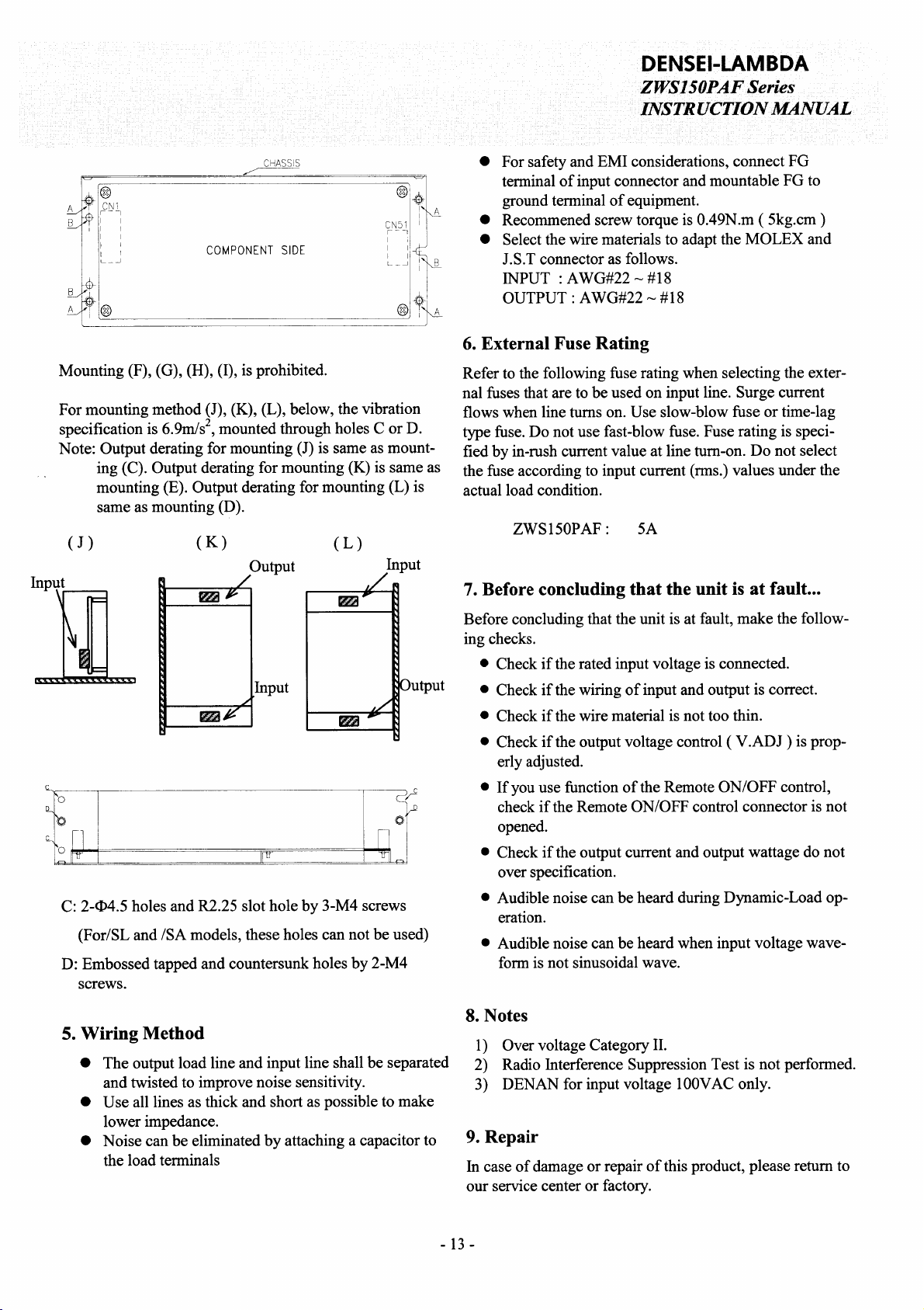
4. Mounting Directions
4-1. Output Derating according to the Mounting Di-
rections
Recommended standard mounting method is ( A ). Method
( B ), ( C ), ( D ), ( E ) are also possible. Mounting (F), (G)
are prohibited. Please do not use installation method ( F ),
where the PCB will be on the top side and heat will be
trapped inside the unit. Refer to the derating below. In the
following derating curve, average load(%) is percent of
maximum output load (both Maximum Output Current and
Maximum Output Power in specifications). Do not exceed
the load deratings.
PCB type
( A )
With chassis, with chassis&cover type
( B )
( C )
( F )
Prohibit
Standard Mounting
( D )
( E )
( A )
Standard Mounting ( B )
( C ) ( D )
( E ) ( F )
Prohibit
( G )
Prohibit
Co
m
po
n
e
n
t
Input
In
p
ut
Input
Output
Out
p
ut
In
p
ut
Com
p
onent
Input
Input In
p
ut
Output
Out
p
ut
In
p
ut
( H )
Prohibit
( I )
Prohibit

- 11 -
DENSEI-LAMBDA
ZWS150PAF Series
INSTRUCTION MANUAL
Output Derating
• Convection cooling
PCB type and with chassis type
0
20
40
60
80
100
-10 0 10 20 30 40 50 60
Ambient Temperature (°C)
Average Load (%)
Convection Average Load (%)
Mounting
Ta A B C D E
-10~ 40°C 100 100 100 100 100
50°C 100 100 80 80 80
55°C 85 85 70 70 70
60°C 70 70 60 60 60
With chassis and cover type
0
20
40
60
80
100
-10 0 10 20 30 40 50
Ambient Temperature (°C)
Average Load (%)
Convection Average Load (%)
Mounting
Ta A B C D E
-10~ 15°C 100 100 100 100 100
20°C 100 100 95 100 95
30°C 100 80 80 80 80
40°C 80 65 65 65 65
50°C 65 50 56 50 56
• Forced air cooling
PCB type and with chassis type
0
20
40
60
80
100
-10 0 10 20 30 40 50 60 70
Ambient Temperature (°C)
Average Load (%)
Forcedair Average Load (%)
Mounting
Ta A,B,C,D,E
-10~ 60°C 100
70°C 70
With chassis and cover type
0
20
40
60
80
100
-10 0 10 20 30 40 50 60
Ambient Temperature (°C)
Average Load (%)
Forcedair Average Load (%)
Mounting
Ta A,B,C,D,E
-10~ 50°C 100
60°C 70
*Recommended minimum air velocity : 0.7m/s ( Measured
at component side of PCB, air must flow through compo-
nent side).As a reference for forced Air Cooling, let air flow
so that the transformer T1 core temperature is lower than
85°C.
Mounting (A),(B)
Mounting (C),(D),(E)
Mounting
(A),(B),(C),(D),(E)
Mounting (A)
Mounting (B),(D)
Mounting (C),(E)
Mounting
(A),(B),(C),(D),(E)

- 12 -
DENSEI-LAMBDA
ZWS150PAF Series
INSTRUCTION MANUAL
Test point T1
PCB
(CORE)
R7
4-2. Mounting Method
PCB type
Please use the mounting hole (4 holes of φ3.5) and insert
the spacer (MAXφ8.0)of height over 8mm to lift the unit.
Also use all 4 mounting holes for the unit installation. The
vibration spec is the value taken when the unit is raised by
8mm spacers.
Note: For cases where the unit is often under vibration
condition, fix with isolated spacer (non conductive), at the
5th hole, near C6 on the PCB.
The 5th hole diameter: Φ3.5mm
PCB thickness: 1.6mm
Maximum spacer outer diameter: Φ7mm
Example:
Please leave 4mm space from the surfaces and leave
4mm space from the sides of PCB, especially from the
solder surface, 8mm space is necessary. If the space is
not enough, the specification of insulation and withstand
voltage will not be satisfied.
FG should be connected to the earth terminal of the appa-
ratus. If not, the EMI noise and output noise will increase.
Hatching area is maximum permissible area of metal part
for mounting.(9mm from each PCB corners)
For chassis option /L, chassis & cover option /A
Recommended mounting by following holes A or B, to
meet 19.6m/s2 vibration specification.Mounting direction
(F) & (G) is prohibited as shown in section 4-1. The power
supply can be mounted through holes A or B.
A: Embossed tapped and countersunk holes by 4-M4
screws
B: Φ4.5 holes and R2.25 slot hole by 3-M4 screws (For
/SL and /SA models, these holes can not be used)
This manual suits for next models
8
Table of contents


