DG USB3D-IP User manual

dg_usb3.0_dev_ip_demo_instruction_en.doc
15 May 2015 Page 1
USB3D
USB3DUSB3D
USB3D-
--
-IP (USB3.0
IP (USB3.0IP (USB3.0
IP (USB3.0-
--
-Device function IP) demo manua
Device function IP) demo manuaDevice function IP) demo manua
Device function IP) demo manua
Rev 1.3E / 15 May, 2015
This document describes USB3D-IP (USB3.0 device function IP-Core) eva uation procedure using A tera
eva uation board (Cyc oneIV GX board, Cyc oneVE board, and ArriaV GX starter board) or Xi inx
eva uation board (SP605, ML605, KC705, and ZC706 board) and USB3.0 adapter board with eva uation
sof-fi e or bit-fi e
1
11
1.
..
.Eva uation Environment
Eva uation EnvironmentEva uation Environment
Eva uation Environment
This demo design operates under fo owing environment shown at
Figure 1.
..
.
1
11
1-
--
-1
11
1A tera Environment
A tera EnvironmentA tera Environment
A tera Environment
For A tera USB3.0 Device-IP eva uation, user must arrange fo owing environment.
•A tera eva uation board (Cyc one IV GX board in this examp e)
•USB3.0 adapter board from DesignGateway [Part# AB08-USB3HSMC]
•USB3.0 A to A cab e attached with adapter board.
•A tera sof-fi e down oad too (programmer) and NiosII conso e.
•Host PC with USB3.0 port. (PCIe extension USB3.0 host card is a so avai ab e, however, such PCIe
extension host card is sensitive to ana og characteristics such as error occurrence at some PCIe s ot
position. And PCIe extension host card cannot provide enough transfer performance when PCIe
interface is 1- ane and not GEN2 but GEN1 speed because GEN1 1- ane PCIe I/F imits its
performance to 2.5Gbps=200Mbyte/s at maximum.)
Figure
Figure Figure
Figure 1
11
1: A tera demo environment for USB3D
: A tera demo environment for USB3D: A tera demo environment for USB3D
: A tera demo environment for USB3D-
--
-IP eva uation
IP eva uationIP eva uation
IP eva uation
(Notes) Eva uation sof-fi e has 1-hour time imit operation after FPGA configuration.

dg_usb3.0_dev_ip_demo_instruction_en.doc
15 May 2015 Page 2
1
11
1-
--
-2
22
2
Xi inx
Xi inxXi inx
Xi inx
Environment
EnvironmentEnvironment
Environment
For Xi inx USB3.0 Device-IP eva uation, user must arrange fo owing environment.
•Xi inx eva uation board (SP-605 in this examp e)
•USB3.0 adapter board from DesignGateway [Part# AB07-USB3FMC]
•USB3.0 A to A cab e attached with adapter board.
•Xi inx bit-fi e down oad too (iMPACT) and seria conso e such as Teraterm.
•Host PC with USB3.0 port. (PCIe extension USB3.0 host card is a so avai ab e, however, such PCIe
extension host card is sensitive to ana og characteristics such as error occurrence at some PCIe s ot
position. And PCIe extension host card cannot provide enough transfer performance when PCIe
interface is 1- ane and not GEN2 but GEN1 speed because GEN1 1- ane PCIe I/F imits its
performance to 2.5Gbps=200Mbyte/s at maximum.)
Figure
Figure Figure
Figure 2
22
2: Xi inx d
: Xi inx d: Xi inx d
: Xi inx demo environment for USB3D
emo environment for USB3Demo environment for USB3D
emo environment for USB3D-
--
-IP eva uation
IP eva uationIP eva uation
IP eva uation
(Notes) Eva uation bit-fi e has 1-hour time imit operation after FPGA configuration.
dg_usb3.0_dev_ip_demo_instruction_en.doc
15 May 2015 Page 3
2
22
2.
..
.Eva uation procedure
Eva uation procedureEva uation procedure
Eva uation procedure
2
22
2-
--
-1
11
1A tera E
A tera EA tera E
A tera Eva uation Procedure
va uation Procedureva uation Procedure
va uation Procedure
For A tera USB3.0 Device-IP eva uation, fo ow eva uation procedure be ow.
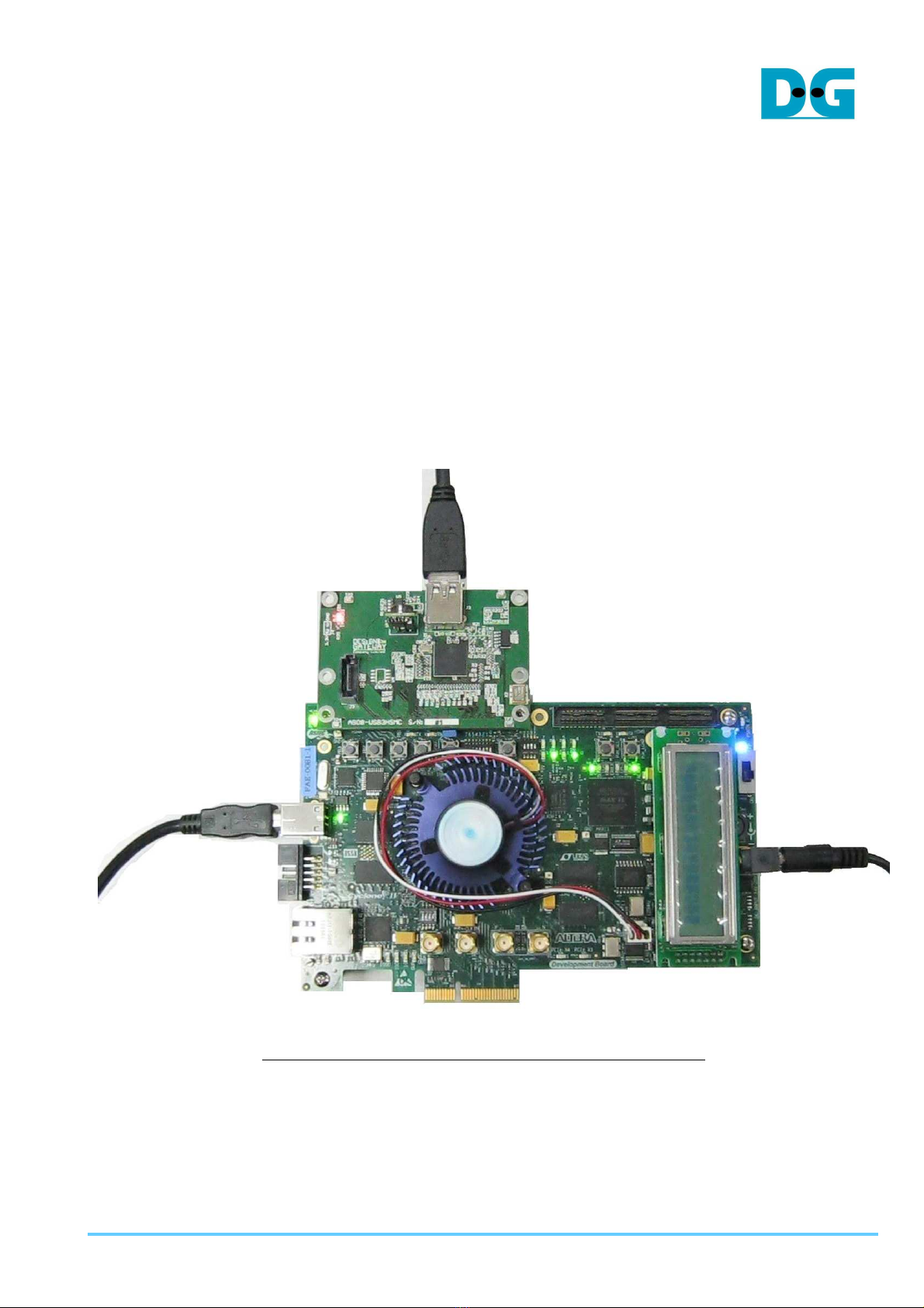
•Check that both A tera board (Cyc oneIV GX/Cyc oneVE/ArriaV GX starter board) and adapter
board are powered off.
•Connect USB Cab e to USB connector on A tera board (J4 for Cyc oneIV GX board/J10 for
Cyc oneVE board/J14 for ArriaV GX starter board) for JTAG programming and JTAG UART
operation.
•Set HSMC interface vo tage of Cyc oneIV GX board to 2.5V. (Short J3 header. Refer to Cyc oneIV GX
board manua for more detai .)
•Connect adapter board (AB08-USB3HSMC) to HSMC connector.
•Confirm that JP1 on the adapter board is not jumped (OFF).
•Connect USB3.0 AtoA cab e with USB connector on the adapter board.
•Connect opposite side of USB3.0 AtoA cab e to the USB3.0 connector of the Host PC.
Figure
Figure Figure
Figure 3
33
3: Adapter board connection to Cyc oneIV GX
: Adapter board connection to Cyc oneIV GX : Adapter board connection to Cyc oneIV GX
: Adapter board connection to Cyc oneIV GX board
boardboard
board

dg_usb3.0_dev_ip_demo_instruction_en.doc
15 May 2015 Page 4
Figure
Figure Figure
Figure 4
44
4: Adapter board connection to Cyc oneVE board
: Adapter board connection to Cyc oneVE board: Adapter board connection to Cyc oneVE board
: Adapter board connection to Cyc oneVE board
Figure
Figure Figure
Figure 5
55
5: Adapter board connection to ArriaV GX starter board
: Adapter board connection to ArriaV GX starter board: Adapter board connection to ArriaV GX starter board
: Adapter board connection to ArriaV GX starter board

dg_usb3.0_dev_ip_demo_instruction_en.doc
15 May 2015 Page 5
•Power up a boards, run ALTERA Programmer on the PC, and down oad eva uation sof-fi e to the
FPGA. After down oad finish, c ose Programmer software. (At this timing, (FPGA operation is
a ready running and FPGA is waiting JTAG UART output.)
•Run nios2-termina from “ALTERA NIOS2 Command She ” as be ow Figure 6.
Figure
Figure Figure
Figure 6
66
6: start nios2
: start nios2: start nios2
: start nios2-
--
-termina
terminatermina
termina
•When JTAG UART starts its operation, it shows message as Figure 7. If nios2-termina cannot start
or this message is not appeared, check USB cab e or down oad settings of Programmer.
Figure
Figure Figure
Figure 7
77
7: Device operation start message
: Device operation start message: Device operation start message
: Device operation start message
dg_usb3.0_dev_ip_demo_instruction_en.doc
15 May 2015 Page 6
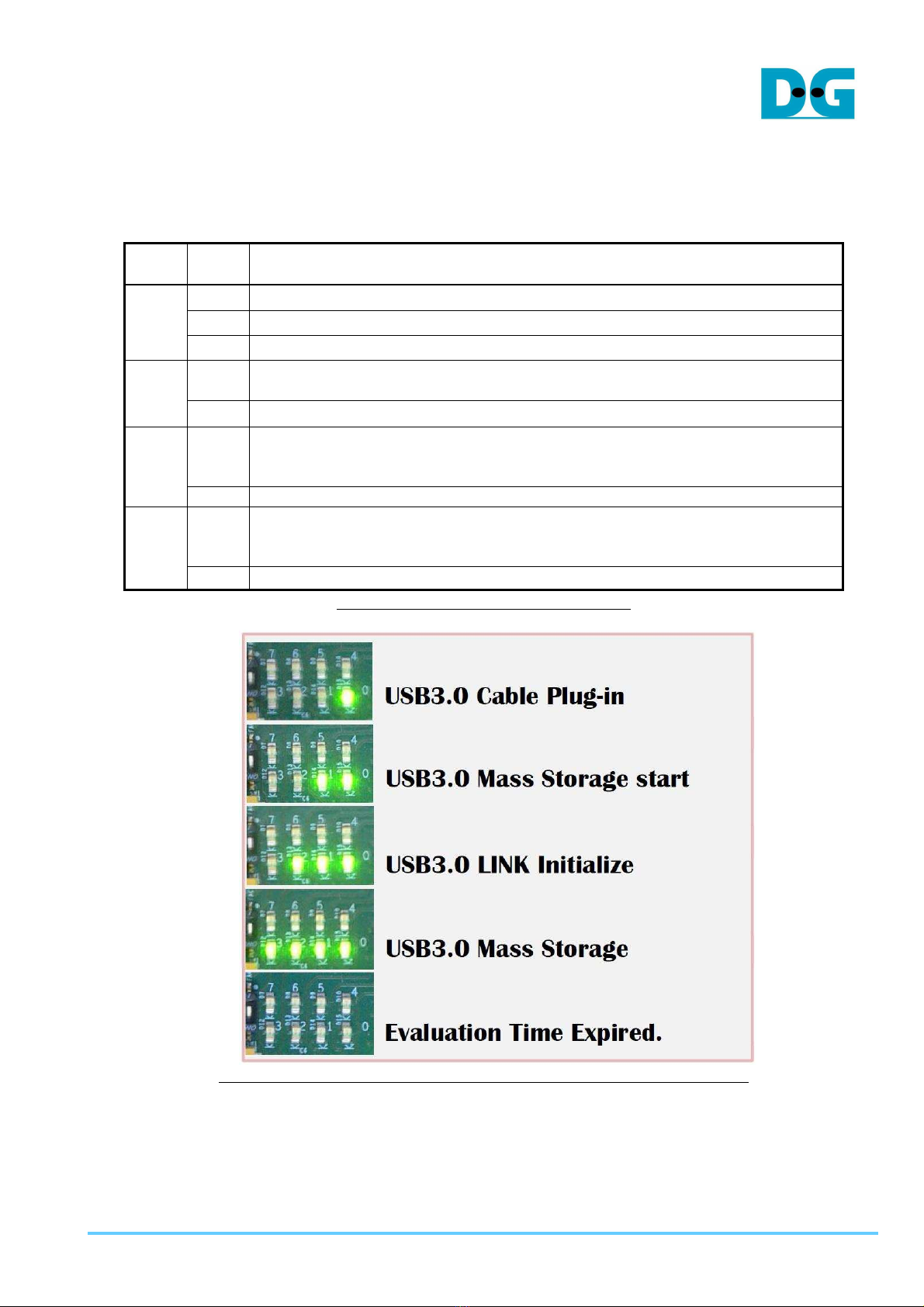
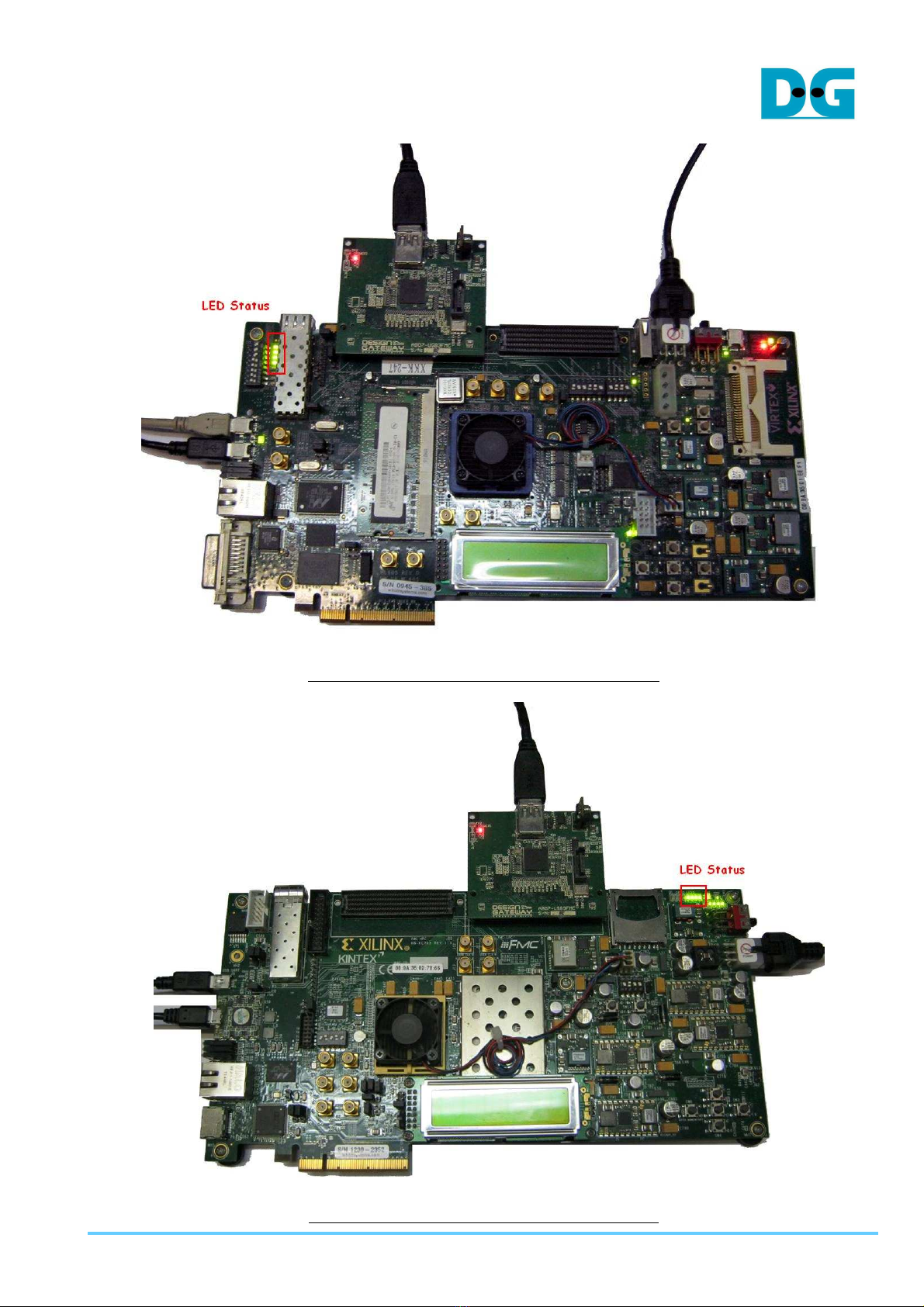
•After sof-fi e down oad finish and JTAG UART operation start, check USER_LED0-3 status near by
HSMC connector on the A tera board. See Tab e 1 for LED definition. Note that LED0 b inks and
other LEDs are OFF when USB cab e is unp ugged. When USB cab e is connected again, LED wi
change its state as shown in Figure 8.
LED
LEDLED
LED
Statu
StatuStatu
Statu
s
ss
s
Description
DescriptionDescription
Description
LED0
OFF
A tera
FPGA configuration is not comp eted.
B ink
VBUS is not detected. USB cab e is not p ugged correct y for examp e.
ON
USB cab e is p ugged correct y and FPGA detects VBUS presence.
LED1
OFF
USB
3.0 Mass Storage C ass operation is not started yet.
A tera board might have prob em such as memory initia ization fai .
ON
USB3.0 Mass Storage C ass operation is started successfu y.
LED2
OFF
Cannot initia ize USB3.0 LINK process.
Check HSMC connection of the demo board.
Check that USB3.0 cab e is the demo board attached cab e.
ON
USB3.0 LINK initia ization comp eted successfu y.
LED3
OFF
USB3.0 Mass Storage C ass detection by HostPC is not comp eted.
It is possib e that signa qua ity prob em exists in the host USB3.0 adapter or
device driver has some prob em.
ON
USB3.0 Mass Storage C ass detection by HostPC is comp eted successfu y.
Tab e
Tab e Tab e
Tab e 1
11
1: LED definition of A tera board
: LED definition of A tera board: LED definition of A tera board
: LED definition of A tera board
Figure
Figure Figure
Figure 8
88
8: USB3.0 dev
: USB3.0 dev: USB3.0 dev
: USB3.0 device operation LED
ice operation LEDice operation LED
ice operation LED0
00
0-
--
-LED3
LED3LED3
LED3
status on
status on status on
status on A tera
A teraA tera
A tera
board
boardboard
board
※ A LED wi be OFF when 1-hour time imitation is expired.
dg_usb3.0_dev_ip_demo_instruction_en.doc
15 May 2015 Page 7
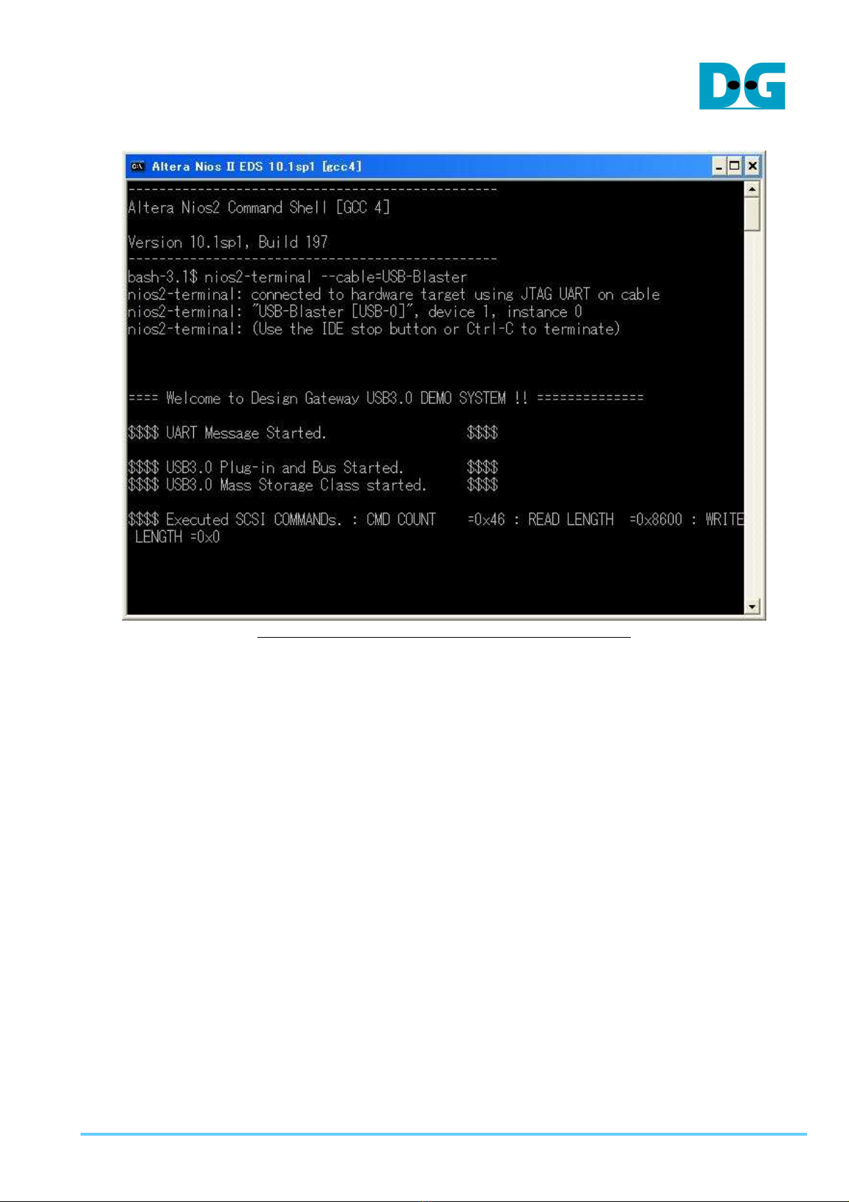
•After FPGA operation starts, at east fo owing Figure 9 message wi appear on the seria conso e.
Figure
Figure Figure
Figure 9
99
9: Mass Storage C ass operation start message
: Mass Storage C ass operation start message: Mass Storage C ass operation start message
: Mass Storage C ass operation start message
dg_usb3.0_dev_ip_demo_instruction_en.doc
15 May 2015 Page 8
2
22
2-
--
-2
22
2Xi inx
Xi inxXi inx
Xi inx
E
EE
Eva uation Procedure
va uation Procedureva uation Procedure
va uation Procedure
For Xi inx USB3.0 Device-IP eva uation, fo ow eva uation procedure be ow.
•Check that both Xi inx board (SP605/ML605/KC705/ZC706 board) and adapter board are powered
off.
•a) SP605/ML605: Connect USB mini-cab e#1 to USB mini-connector on Xi inx board (J4 for
SP605/J22 for ML605) for JTAG programming.
b) KC705/ZC706: Connect USB micro cab e to USB micro connector on Xi inx board (U29 for
KC705/U30 for ZC706) for JTAG programming.
•Connect USB mini-cab e#2 to USB mini-connector on Xi inx board (J23 for SP605/J21 for ML605/J6
for KC705/J21 for ZC706) for seria conso e I/F on HostPC.
•Confirm that FMC interface vo tage is 2.5V, and then connect adapter board (AB07-USB3FMC) to
the FMC-LPC connector on Xi inx board.
•Confirm that JP1 on the adapter board is not jumped (OFF).
•Connect USB3.0 AtoA cab e with USB connector on the adapter board.
•Connect opposite side of USB3.0 AtoA cab e to the USB3.0 connector of the Host PC.
Figure
Figure Figure
Figure 10
1010
10: Adapter board connection to SP605
: Adapter board connection to SP605: Adapter board connection to SP605
: Adapter board connection to SP605
dg_usb3.0_dev_ip_demo_instruction_en.doc
15 May 2015 Page 9
Figure
Figure Figure
Figure 11
1111
11: Adapter board connection to ML605
: Adapter board connection to ML605: Adapter board connection to ML605
: Adapter board connection to ML605
Figure
Figure Figure
Figure 12
1212
12: Adapter board connection to KC705
: Adapter board connection to KC705: Adapter board connection to KC705
: Adapter board connection to KC705

dg_usb3.0_dev_ip_demo_instruction_en.doc
15 May 2015 Page 10
Figure
Figure Figure
Figure 13
1313
13: Adapter board connection to ZC706
: Adapter board connection to ZC706: Adapter board connection to ZC706
: Adapter board connection to ZC706
•Power up a demo device, run seria termina (TeraTerm for examp e) and set fo owing
communication parameter
Baud Rate = 115,200 Data = 8bit Stop Bit = 1 Parity = None
•a) Start iMPACT and down oad eva uation bit-fi e to FPGA.
b) For ZC706 board on y, set SW11=”00000” to configure PS from JTAG, and set SW4=”01” to connect
JTAG to USB-to-JTAG interface, as shown in Figure 14 and Figure 15. After that, open ISE
command prompt and run bat fi e to down oad bit-fi e and e f-fi e to FPGA, as shown in Figure 16.
Figure
Figure Figure
Figure 14
1414
14: SW11 setting on ZC706 board
: SW11 setting on ZC706 board: SW11 setting on ZC706 board
: SW11 setting on ZC706 board
Figure
Figure Figure
Figure 15
1515
15: SW4 setting on ZC706 board
: SW4 setting on ZC706 board: SW4 setting on ZC706 board
: SW4 setting on ZC706 board

dg_usb3.0_dev_ip_demo_instruction_en.doc
15 May 2015 Page 11
Figure
Figure Figure
Figure 16
1616
16: Run bat fi e to program bit and e f fi e on ZC706 board
: Run bat fi e to program bit and e f fi e on ZC706 board: Run bat fi e to program bit and e f fi e on ZC706 board
: Run bat fi e to program bit and e f fi e on ZC706 board
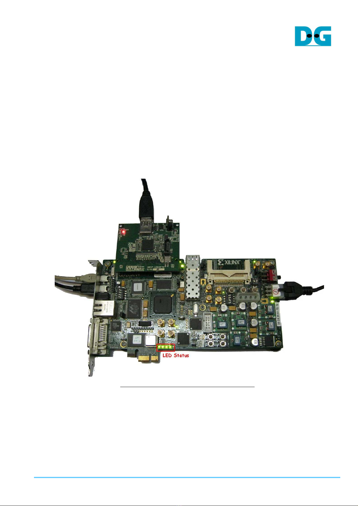
•After bit-fi e down oad finish, check GPIO_LED0-3 status on Xi inx board. See tab e-2 for LED
definition. Note that LED0 b inks and other LEDs are OFF when USB cab e is unp ugged. When
USB cab e is connected again, LED wi change its state as shown in Figure 17.
LED
LEDLED
LED
Light
LightLight
Light
Description
DescriptionDescription
Description
DS3
/LED0
OFF
SP
-
605 FPGA con
figuration is not comp eted.
B ink
VBUS is not detected. USB cab e is not p ugged correct y for examp e.
ON
USB cab e is p ugged correct y and detects VBUS presence.
DS4
/LED1/
R
OFF
USB3.0 Mass Storage C ass operation is not started yet.
SP-605 board might have prob em such as memory initia ization fai .
ON
USB3.0 Mass Storage C ass operation is started successfu y.
DS5
/LED2/C
OFF
Cannot initia ize USB3.0 LINK process.
Check FMC connection of the demo board.
Check that USB3.0 cab e is the demo board attached cab e.
ON
USB3.0 LINK initia ization comp eted successfu y.
DS6
/LED3/L
OFF
USB3.0 Mass Storage C ass detection by HostPC is not comp eted.
It is possib e that signa qua ity prob em exists in the host USB3.0 adapter or
device driver has some prob em.
ON
USB3.0 Mass Storage C ass detection by HostPC is comp eted successfu y.
Tab e
Tab eTab e
Tab e-
--
-2:
2: 2:
2: LED
LEDLED
LED
definition of SP605 board
definition of SP605 boarddefinition of SP605 board
definition of SP605 board
Figure
Figure Figure
Figure 17
1717
17: USB3.0 device operation LED status on SP605 board
: USB3.0 device operation LED status on SP605 board: USB3.0 device operation LED status on SP605 board
: USB3.0 device operation LED status on SP605 board
※ A LED wi be OFF when 1-hour time imitation is expired.
dg_usb3.0_dev_ip_demo_instruction_en.doc
15 May 2015 Page 12
•After FPGA operation starts, at east fo owing Figure 18 message wi appear on the seria conso e.
(same meaning of DS4). If Figure 18 message does not appear, check seria (USB mini) cab e as we as
seria communication parameters.
Figure
Figure Figure
Figure 18
1818
18: Device operation start message
: Device operation start message: Device operation start message
: Device operation start message
•When communication with HostPC is successfu y started, fo owing Figure 19 message wi appear
on the seria conso e (same meaning of DS6).
Figure
Figure Figure
Figure 19
1919
19: Mass Storage C ass operation start message
: Mass Storage C ass operation start message: Mass Storage C ass operation start message
: Mass Storage C ass operation start message
dg_usb3.0_dev_ip_demo_instruction_en.doc
15 May 2015 Page 13
3
33
3.
..
.Demo operation examp e
Demo operation examp eDemo operation examp e
Demo operation examp e
•The demo design emu ates genera USB removab e drive so that user can check same functions and
operations. However, the demo design has fo owing imitation.
(1) The demo design uses on-board 128Mbytes DDR memory and assigns 127Mbytes as a storage
memory space.
(2) Because storage memory is vo ati e, stored data on the DDR memory wi be disappeared when
power is off and user must execute format after every power cyc e.
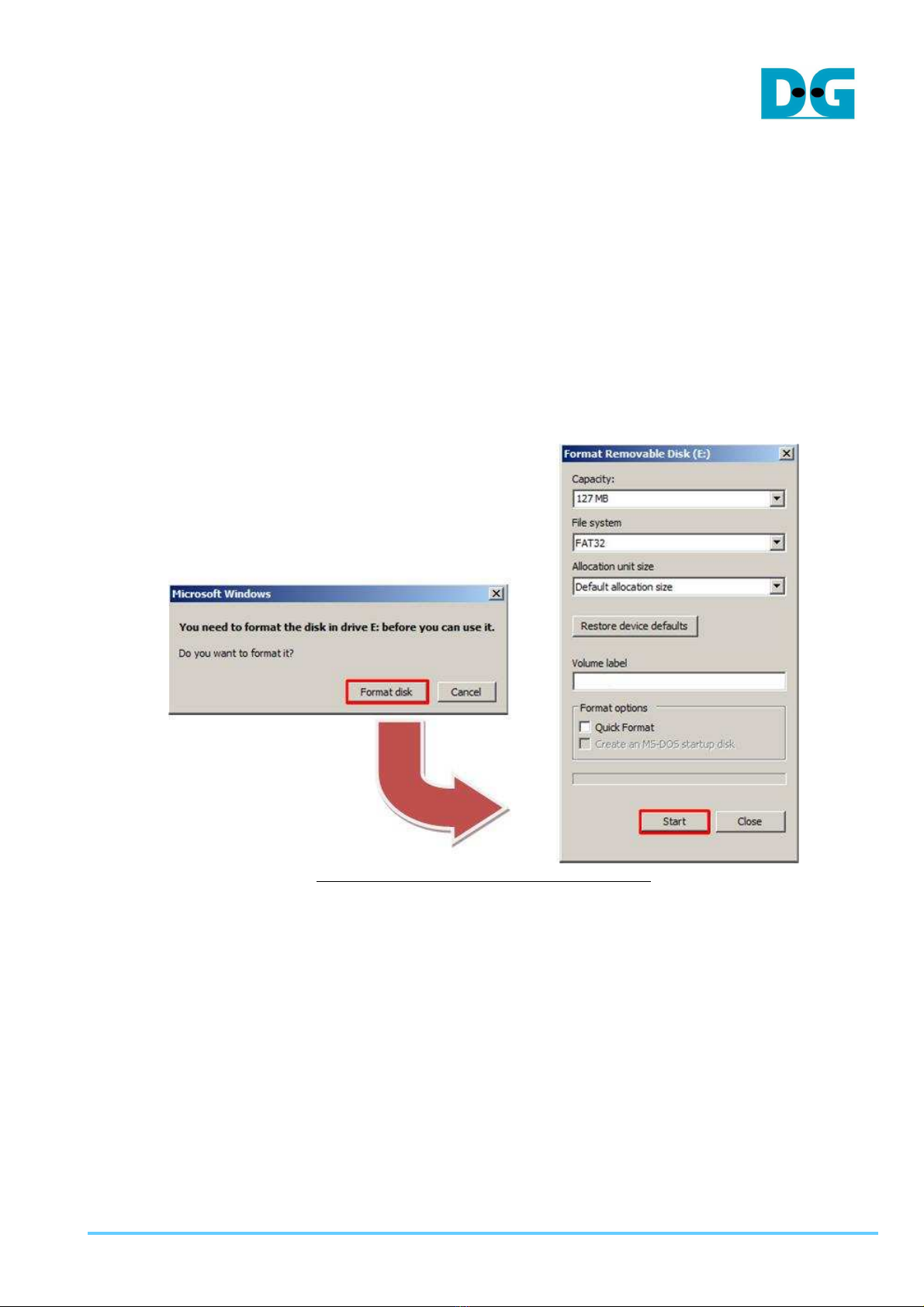
1. Windows on the HostPC wi first y request format after power cyc e of demo design.
So user must execute norma format operation.
If Windows does not show message, then execute format manua y, however in this case, enough
care must be taken not to format incorrect drive.
DesignGateway is not responsib e for any troub e or prob em caused by such incorrect operation.
DesignGateway is not responsib e for any troub e or prob em caused by such incorrect operation.DesignGateway is not responsib e for any troub e or prob em caused by such incorrect operation.
DesignGateway is not responsib e for any troub e or prob em caused by such incorrect operation.
Figure
Figure Figure
Figure 20
2020
20:
: :
: Execute format to the demo drive
Execute format to the demo driveExecute format to the demo drive
Execute format to the demo drive

dg_usb3.0_dev_ip_demo_instruction_en.doc
15 May 2015 Page 14
2. Device Manager
User can confirm by the device manager of Windows that demo drive is recognized as an USB
mass storage device.
Figure
Figure Figure
Figure 21
2121
21: Mass Storage USB Device detected from Device Manager
: Mass Storage USB Device detected from Device Manager: Mass Storage USB Device detected from Device Manager
: Mass Storage USB Device detected from Device Manager
3. Copy & Paste
User can execute fi e or fo der Copy&Paste to the demo drive for examp e.
Note that drive capacity is imited to 127Mbytes on y.
Figure
Figure Figure
Figure 22
2222
22: Copy & Paster
: Copy & Paster: Copy & Paster
: Copy & Paster
dg_usb3.0_dev_ip_demo_instruction_en.doc
15 May 2015 Page 15
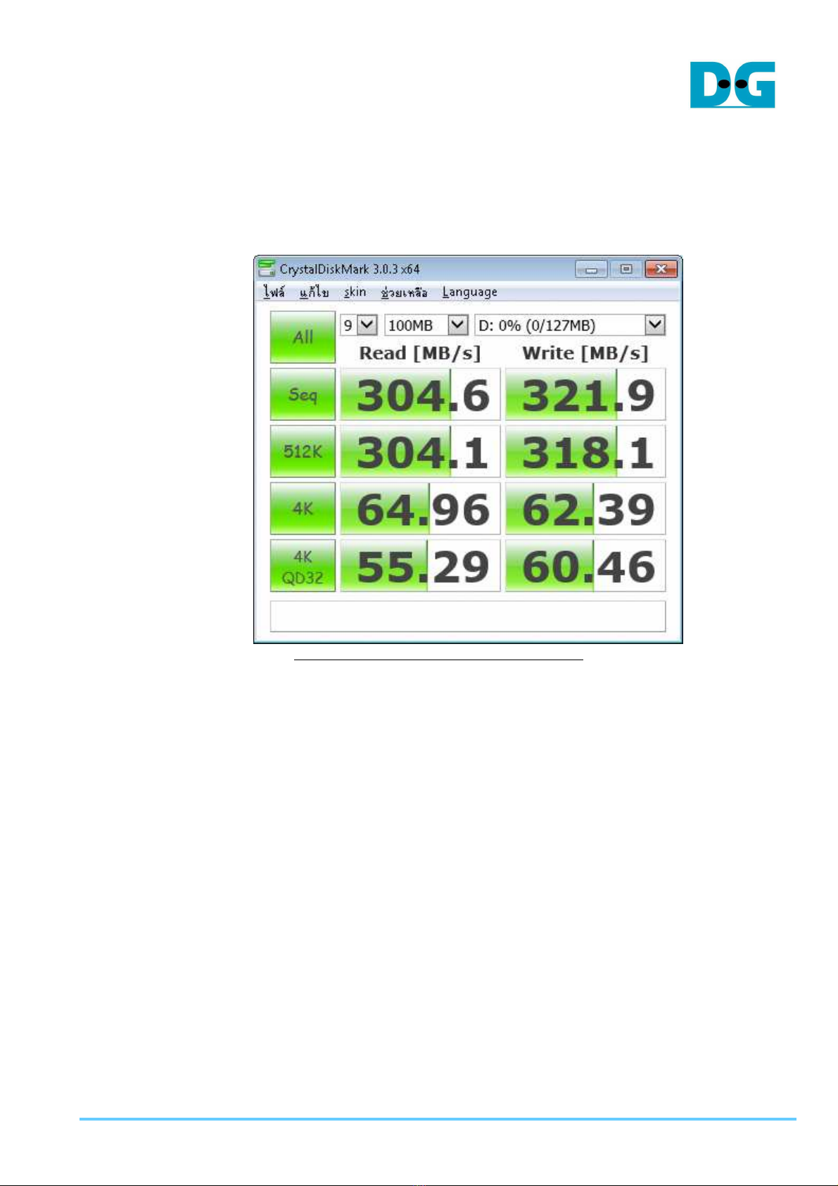
4. Benchmark test
User can execute benchmark test to check performance.
Note that if HostPC performance is poor (for examp e of 1- ane PCIe adapter usage or PCIe is
GEN1 case), demo drive cannot provide USB3.0 performance. Rea transfer performance depends
on OS type on the HostPC, CPU performance, and/or PCIe bus speed of the USB3.0 adapter card.
Figure
Figure Figure
Figure 23
2323
23: Benchmark test resu t examp e
: Benchmark test resu t examp e: Benchmark test resu t examp e
: Benchmark test resu t examp e
5. P ug-out and P ug-in
The demo drive can execute p ug-out and p ug-in operation as a removab e disk.
Take enough interva s between p ug-out and p ug-in for correct operation.
If user execute p ug-in immediate y after p ug-out, HostPC may not detect USB3.0 device
correct y.

dg_usb3.0_dev_ip_demo_instruction_en.doc
15 May 2015 Page 16
4
44
4.
..
.
Revision History
Revision HistoryRevision History
Revision History
Revision
Date
Description
1.0
18
-
Ju
-
2012
Re ease
Eng ish version.
1.1E
04
-
Mar
-
2015
Merged both A tera and Xi in
x into one document
1.2E
09
-
Mar
-
2015
Updated Figure
-
15 by the atest test resu t
1.3E
15
-
May
-
2015
Add board support
Copyright: 2012 Design Gateway Co,Ltd.
Table of contents
Other DG Motherboard manuals


