EEZ H24005 Instruction Manual

EEZ PSU H24005 Building Instructions (r5B9)
Work in progress – please note that some of issues discussed below is fixed in r5B10 and newer revi-
sions
•PCB assembly
•Enclosure and wire harness
•Firmware uploading
1. PCB assembly
The PSU has four PCBs where SMT parts are used to the greatest extent Only connectors and few
specialized parts (e g power resistor, PCB mounted AC/DC adapter, post-regulator's power mosfet,
etc ) are THT
SMT parts are selected to be easily mounted with hand soldering and assistance of magnifying glass
with light or low magnification microscope In general, a magnification of x8 to x10 should be more then
appropriate for this task Almost all passive components are of 0805 size and never smaller then 0603
Selected IC packages are SOIC, TSOP, TSSOP and similar that have exposed pins (i e no QFN or
BGA package are selected)
Only two ICs (IC1, IC16) that has exposed power tab cannot be simply mounted with soldering iron and
need hot air soldering station That requires different skills but one can find many useful videos on the
Internet with instructions how to do that efficiently at home without use of e g stencil and reflow owen
1.1. Re uired tools
•Soldering iron with conical sloped tip example
•Hot air soldering station example
•Solder wire 0 25 mm example, and 0 7 mm example (optionally solder paste, for ICs with
1
Fig 1: Stacked assembled EEZ PSU H24005 in acryl and metal enclosures

EEZ PSU H24005 building instructions (r5B9)
exposed power tabs but take into account that its shelf life is very limited even when
refrigerated, therefore use small package, example)
•Solder wick / desoldering braid example
•Flux example
•Magnifying glass with light (desktop magnifier with backlight) example or microscope example
•Self-locking tweezers example
•Set of tweezers example1, example2
•Isopropyl alcohol example and paper wipes example for cleaning
•PCB holder example
1.2. Test and measurement e uipment
The basic tool used for measurement is an oscilloscope But, if assembling is performed carefully, that
no single mistake has been done, (e g wrong part value or place, etc ) a simple DMM will be enough to
check basic functionality
During testing and taking measurements please take into account that channel’s negative output
(OUT-) is NOT on ground potential Therefore if you are using multichannel oscilloscope without iso-
lated channels (that is default!) you cannot concurrently connect test probe ground of one channel to
the PGND and another one to OUT- That will interfere with normal operation of CC control loop (IC7,
IC8) because the current sense resistor (R69) will be shorted in that way
1.3. Where to start?
The total number of parts that have to be soldered is almost 800 On the first sight that can easily dis-
courage many, but it's not so bad First, two most demanding PCBs for power boards are identical and
you can try to assemble it side by side following steps mentioned below The AUX PS is the simplest
one but also has AC mains section that require additional care when operating Finally, physically the
biggest one – Arduino Shield is modestly populated but also carry extra parts such as TFT touch-screen
display, Arduino board, binding posts, etc that dictate some other set of assembling rules
A good start could be to check that all parts from the consolidated BOM are available and sorted by
type and values and can be easily accessible As you have probably already learned, simple SMT parts
with 2-3 terminals (passives, diode, transistors) can be easily lost even if you have well arranged and
clean benchtop Therefore instead of crying for lost one, simply order few parts more and take another
one when previously selected was just gone That issue is present with both self-locking and regular
tweezers
There is a few methods of storing and sorting SMT parts like small part snapboxes, envelopes etc
Each of them is valuable as far as it can reduce possibility of replacing one part mistakenly with an-
other That is especially important for ceramic capacitors (MLCCs) that do not carry value marks
A discipline of selecting a single value at the time (even in larger quantity) and placing them on proper
places is of a paramount importance to ensure that PCBs are assembled correctly and will work prop-
erly
When needed tools, bare PCBs and SMT parts are on disposal, one important task still remain before
we can start with PCB assembling – it's how to identify part value since PCB's silkscreens (top and bot -
tom) only carry reference designators (i e R , C , IC , etc )
If you are using Eagle then open .brd file and when populating top layer make sure that among other
layers 21, 25, and 27 are visible (see Top assembly selected layers png) For assembling bottom layer
set layers 22, 26, and 28 as visible (see Bottom assembly selected layers png)
The freeware edition of Eagle also allows you to open brd file and switch layers on and off
When installation of the Eagle is not an option, you can use the following images:
•AUX PS r5B9 assembly (top layer) png
•AUX PS r5B9 assembly (bottom layer) png
•Arduino shield r3B4 assembly (top layer) png
•Arduino shield r3B4 assembly (bottom layer) png
•Power board r5B9 assembly (top layer) png
•Power board r5B9 assembly (bottom layer) png
Above mentioned order of PCBs is not mandatory for assembling process but represents a logical se-
quence since AUX PS is required for powering Arduino shield and Arduino shield is required for control-
ling Power boards Suggested order is also sorted by PCB complexity starting with the simplest one
If not otherwise specified, we'd like to recommend that parts are soldered in the following order on the
2
EEZ PSU H24005 building instructions (r5B9)
same layer:
•Small SMT parts (e g passives, diodes, transistors, etc )
•SMT ICs
•Bulk SMT parts (elco capacitors, power inductors, mosfets and diodes) and
•THT parts (connectors, switches, chokes, etc )
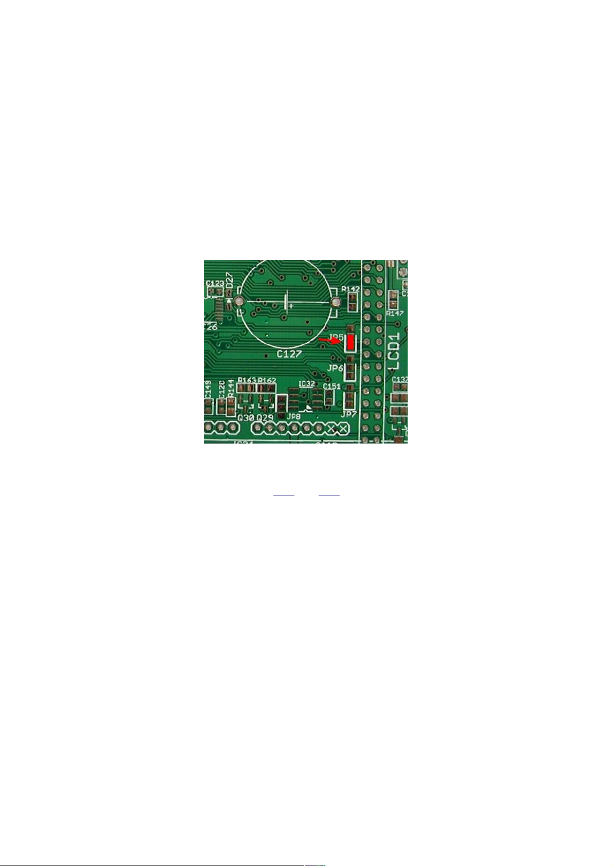
1.4. Default jumper positions
For various reason on few places on the PCBs a jumpers section are used where zero-ohm resistor is
used to define signal path Some of them define behavior of the circuits (e g JP5, JP6, and JP7) and
when wired in wrong way or left unpopulated that can create some difficulties and the firmware could
not control it properly To simplify a whole assembly process a clear mark is added next to zero-ohm re-
sistor default position that should insure a proper functionality with current firmware revision On the pic-
ture below above mentioned jumper sections are shown and red rectangle indicate the place for zero-
ohm resistor that is in line with “U” shaped mark
1.5. AUX PS r5B9 assembling
Schematic for this board is shown on sheets 6/12 and 7/12 We'd like to recommend the following steps
for assembling this board:
•+5 V power supply built around IC16
•Fan control (Q22, X6)
•AC input terminal and protection
•Soft start/stand-by (Q20, Q21, OK1, OK2)
•AC/DC module (TR2) and
•Ethernet and USB terminals (X7, X11)
The IC16 is one of the few parts that require hot air soldering because of exposed power tab placed be-
neath its plastic body It has to be mounted in that way to establish a solid electrical and thermal bond
with exposed copper on the PCB's top layer Otherwise, a permanent damage may occur or erratic op-
eration Due to that this part should be mounted first When that is done we can proceed with comple-
tion of +5 V power supply section The X5 connector has to be mounted after surrounding SMT parts
(D21, R130, R131) otherwise it could be difficult to mount them without damaging X5 by touching it un -
intentionally with soldering iron body or tip
When this section is finished and ready for testing do not solder TR2 since it's huge and could make
mounting of surrounding parts afterward almost impossible Instead, use external regulated 12 V supply
and connect it properly on its terminal 9- and +7 If everything is soldered correctly, a regulated +5 V will
appear on X5 pin 10 (+) and 9 (-)
Now we can proceed with fan control Keep in mind to mount THT part at the end (X6) Testing of this
section has to be postponed until Arduino Shield is assembled Also, it will require preparation of fan ca-
ble which comes without connector
AC input terminal and protection section contains only THT parts that can be carefully soldered on the
bottom layer
3
Fig 2: Zero-ohm jumpers markings

EEZ PSU H24005 building instructions (r5B9)
Soft start/stand-by triacs Q20 and Q21 are sharing the same heatsink KK1 mounted on its opposite
sides using single screw and nut (Fig 3) They can be mounted on before soldering Another possibility
is to solder heatsink first and then mount on each side a triac and then solder their terminals Take care
that power resistor R107 is of proper type (wirewound) and power rating
Finally, place TR2 as the latest part on the top PCB layer Now it's possible to test once again +5 V
power supply by carefully applied AC mains on the X4 pin 1, 2 and 5
On the bottom layer only two parts have to be mounted – Ethernet (X7) and USB (X11) terminals If you
got customized enclosure with pre-drilled holes on its rear panel, we recommend to mount the PCB on
the rear panel first (using 14 mm spacers) and then solder that terminals That will insure that every-
thing fits perfectly
1.6. Arduino Shield r3B4 assembling
There is no recommended order in which sections on this PCB should be soldered One possibility is to
simply follow the order of sheets in consolidated schematics related to this board (sheet 8/12, 9/12,
10/12, 11/12, and 12/12) and to leave the following parts for the end:
•Power relays (K_SER, K_PAR) due to their dimensions
•Super capacitor (C127) for RTC backup
•Push-in connectors (X12, X14) especially if you'd like to follow suggestion to adjust its distance
from the front panel as described below
•40-pin connector (LCD1) for the TFT touch-screen display
•Front panel power switch (SW1)
The revision r3B4 has few issues that we didn't spot before it went into manufacturing but fortunately all
of them can be easily fixed
Red LED polarity
Let's starts with the simplest one which is related to chosen red color LEDs that are located on the
PCB's bottom layer Polarity marking on the PCB is not in line with HSMH-C170 specification Therefore
you simply need to rotate it while soldering
4
Fig 3: Q20 and Q21 shares the same heatsink

EEZ PSU H24005 building instructions (r5B9)
Output capacitors mounting
We are using SMT EEEFK1J220P (22 μF) as output capacitors (C106, C111) that are wider in diameter
than THT UPW1J150MED (15 μF) initially specified The SMT pads provided on that positions are also
for SMT capacitors smaller in diameters Regardless of that, mentioned type can be easily mounted by
simply bending its terminals when it becomes a THT Now, holes for a THT part can be used for solder-
ing
Additional output capacitors
An additional capacitor is recommended on the power output A ceramic 1 μF, 50 V capacitor is used
and damped with 1 Ω resistor They should be placed as close as possible to the output binding post
holes but there is no predicted place for that on this PCB revision Nevertheless it's simple to add them
as it is shown on Fig 5 (Note: Place for this RC pair is added in r5B10)
When lower output ripple is needed it’s possible to mount an elco polymer (e g OS-CON 18 μF, 50 V)
type of capactitor on the opossite PCB side as shown on Fig 6 (Note: Place for this capacitor is added
in r5B12, and above mentioned RC pair is marked as optional)
5
Fig 4: Red LEDs incorrect markings on the Arduino Shield bottom layer
Fig 5: Additional channel's output RC circuit

EEZ PSU H24005 building instructions (r5B9)
Ethernet connector position
The Ethernet connector (X18) is not properly positioned – it is too close to the CH1's heatsink Due to
that it is not possible to insert Ethernet cable that connect output terminal on the rear panel (via X8 on
the AUX PS board)
A right angle connector has to be used as specified in the BOM But, when such connector type is used
(see Fig 7), there is no possibility to put a screw to fix TFT touch-screen display on the lower left corner
viewed from the display's back (or lower right corner viewed from the display's front)
Fortunately that is not a big issue since display still can be fixed on all four corners with 11 mm spacers
and that will provide enough mechanical strength required to withstand finger pressure on that part of
the display (Fig 8)
6
Fig 7: Ethernet header on the Arduino shield
Fig 6: Mounting of elco capacitor between output terminals
EEZ PSU H24005 building instructions (r5B9)
Push-in connectors distance adjustments
Distance between rear side of the front panel and the Arduino Shield PCB is defined by TFT display that
is approx 18 mm:
•5 mm display thickness
•1 5 mm display PCB thickness
•11 mm spacer between display and plastic washer (defined by LCD1 connector height) and
Height of the push-in connectors (X12, X14) is 14 mm and when they are soldered directly on the PCB
they will be 4 mm apart from the front panel surface That does not mean that their pins are not accessi-
ble It's more a question of visual appearance and you can fix that with modified cheap DIL16 sockets
You need to cut them horizontally and insert each half separately since distance between push-in con-
nector's rows is different You also need to adjust their height to 4 mm (usually that is about 5 mm) That
can be done in a matter of minute using a piece of sandpaper
Insert push-in connectors into modified sockets before soldering To improve mechanical strength you
can also apply e g hot glue
Keep in mind that X12 and X14 have to be mounted on the bottom side of the PCB:
7
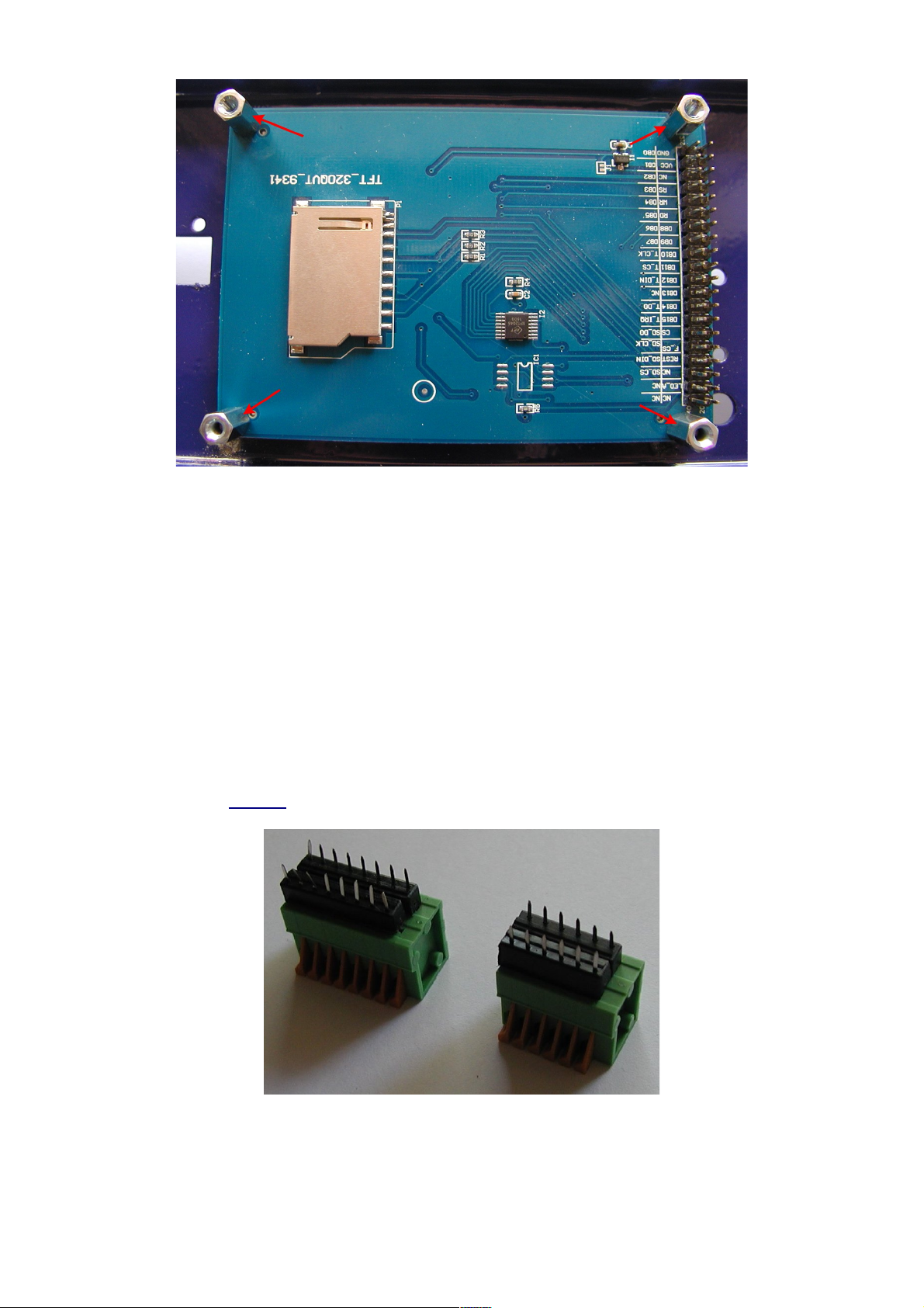
Fig 8: TFT touchscreen display rear view
Fig 9: Push-in connectors with extensions
EEZ PSU H24005 building instructions (r5B9)
The end result looks like this:
When all SMT parts are mounted, followed by THT parts, we can solder few parts mentioned on the be-
ginning:
•The power relay now should not interfere with mounting of any surrounding parts
•The super capacitor is polarized as elco capacitors or battery cell Check its terminals polarity
twice before mounting!
•If push-in connectors X12 and X14 is not inserted into sockets, as it's suggested above, then we
can now proceed with their soldering on the bottom side of the PCB
•TFT touch-screen display connector (LCD1) has to be soldered on the bottom side too If we
want to be completely sure that it's aligned with display, we can mount display on the
customized enclosure first, then insert 40-pin connector on display's header, and finally place
the PCB on top of display Use plastic washer between 11 mm spacers and PCB and another
one between PCB and M3 mounting screw We have to check alignment of the PCB with output
binding posts holes and when everything is in place 40-pin connector can be soldered
•Finally, we can mount power switch (see Fig 12) Once again, it's recommended to see how it's
aligned with the corresponding hole on the enclosure's front panel first, then adjust its position
and start with soldering
8
Fig 10: Push-in connectors mounted on the Arduino shield
Fig 11: Front panel with push-in connectors mounted

EEZ PSU H24005 building instructions (r5B9)
When all parts are mounted and PCB is properly cleaned, an Arduino Due board can be installed It has
to be loaded with appropriate firmware (M2 or newer) that is configured to work with this board revision
Use its USB named Programming port for firmware upload
If everything is assembled correctly and firmware is successfully uploaded, the welcome screen should
appear after reset or new power on The firmware will proceed with self-test and check peripherals and
channels as defined in conf.h, or override with parameters in the user_conf.h file
The AUX PS module r5B9 has mistakenly connected pin 1 of the USB header to the USB cable There -
fore even if the PSU is completely switched off, the Arduino shield will be powered from the external
source if USB cable is connected The easiest way to fix that issue is to detach pin 1 (red) wire and in -
sulated it as shown on the Fig 13
1.7. Power board r5B9 assembling
According to the number of components and functionality, the Power board is the most complex part of
this PSU We'd like to recommend assembling of this board in the following steps:
•Power pre-regulator
9
Fig 13: USB cable hack
Fig 12: Power switch mounting

EEZ PSU H24005 building instructions (r5B9)
•Bias power supply
•Post-regulator
After each section is completed, perform simple testing described below before continuing with the as-
sembling
WARNING: Never apply DC input (+48 V) when AC/DC module is powered on (e.g. connecting ca-
ble manually to the X1 connector). That could generate spikes (due to L1) up to 100 V high that
can easily destroy on-board SMPS controllers (LTC3864 and LM5574)!
Power pre-regulator
The power pre-regulator circuit is shown on Sheet 1/12 We recommend you to start with IC1 that, as in
case of IC14, require soldering of exposed thermal pad A hot air soldering station instead of soldering
iron should be used here This section also require soldering on the PCB’s bottom side (L1 and X1)
That should not be a problem if you are using PCB holder If you choose to supply Power board with AC
instead of DC input, follow Hack #1
Once again, keep in mind to mount all smaller parts first and than continue with bulky one such as L2,
C18, C16, etc
When everything is in place, you can proceed with basic testing Since the board is not fully assembled,
it cannot be done without some tricks The first possible obstacle to check if pre-regulator works prop-
erly is existence of Q3 that is used to enter 100% duty cycle when the pre-regulator is bypassed The
IC1 is then effectively switched off and instead of switching frequency a DC signal will be present on Q1
gate (hence the name 100% duty cycle) But, we’d like to test in this step if switching works or not We
have two possibilities here:
•To apply +5 V (use some external source in this stage) to Q3 gate by soldering a thin wire e g
used for wire wrap to that position or locate pin 13 on IC9 (see Sheet 4/12) and do the same or
•simply place zero-ohm resistor on position R13 Note: don’t forget to remove it before start
testing the Post-regulator section and IC9 is mounted
Before we can apply input power we need to provide some signal on trace OUT+ The easiest way is to
locate any of pins 23 to 26 on X3 connector Do not solder X3 connector in this stage because you’ll
have difficulty with mounting surrounding parts like e g R95, R105, C84, Q19, etc
Again, an external regulated source is needed We can use the same +5 V used to turn on Q3 or some-
thing else with output of up to +40 V In fact, we can start testing by simply connecting OUT+ to the
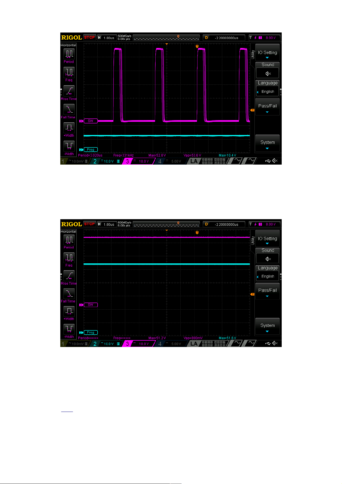
ground If OUT+ is grounded we can check with the scope two points to see if pre-regulator works:
First is “hot-spot” (SW, magenta trace) where Q3 drain, power inductor L2 and D5 cathode are con -
nected Use x10 probe There is also a place for additional R4 and PCB test point ( example) on the
PCB where you can hook probe securely Another test point is PREG_OUT (Preg, cyan trace), output
from the power pre-regulator
Fig 14 shows measurement when +OUT is set to 0 V (grounded) Its output voltage will vary depending
on connected load and difference between post-regulator output, and power pre-regulator output Men -
tioned voltage difference could be about +6 5 V for no load to less then +3 V for full load of 5 A Fig 15
is another example without load when +5 V is used for pre-regulator’s output voltage programming
(measured PREG_OUT is +10 8 V)
10

EEZ PSU H24005 building instructions (r5B9)
Please note that in both cases the SW signal looks erratic but that is only because no load is con-
nected On Fig 16 is shown characteristic switching pattern when load is connected (e g power resis-
tor of 10 Ω)
11
Fig 14: Pre-regulator measurements, +VOUT = 0 V (grounded, no load)
Fig 15: Pre-regulator measurements, +VOUT = 5 V, no load is connected
EEZ PSU H24005 building instructions (r5B9)
Finally on Fig 17 is shown what will happen if Q3 is not turned on The IC1 will enter 100% duty cycle
because chosen values for voltage divider in feedback loop (R12, R15) are set well over pre-regulator
input voltage to 56 V while input voltage is not higher then 50 V
If you’d like to test this scenario be sure that no load is connected, otherwise a Q1 SOA could be easily
exceeded that can damage Q1 permanently (with unknown consequences for IC1 too)
The so-called Low noise mode of operation when pre-regulator works with 100% duty cycle will remove
from channel’s output hard to filter switching noise But working in that mode puts real limitation in out-
put power and if the PSU will be used for application where higher output ripple can be easily tolerated
it’s possible to disable that option by removing Q3 and mount permanently zero-ohm resistor on posi-
tion R13
Bias power supply (switching pre-regulator and LDOs)
The sheet 2/12 has to be followed for bias power supply circuit assembling It does not require any spe-
cial instructions and when everything is in place we can proceed with basic testing Please note that
power pre-regulator will be now also powered and make sure that no load remains connected on the
PREG_OUT from the previous testing Obviously, the first thing that we can test are output voltages on
points +V (IC2), -V (IC3) and +5V (IC5) They should to be within 5 % tolerance +5 V, -5 V and +5 V
Another two points of interest are SW (IC4) and PWRGOOD (IC5) The good place for probing SW sig-
nal is pin 1 on TR1 or D10 cathode Fig 18 shows typical waveform on that point:
12
Fig 17: Pre-regulator in 100% duty cycle, without load connected
Fig 16: Pre-regulator measurements, +VOUT = 5 V with load connected

EEZ PSU H24005 building instructions (r5B9)
It’s interesting to see how the PWRGOOD relates to change of input voltage That signal will be actively
monitored with MCU and it will push the PSU into Stand-by mode as soon as possible when its
changed from high to low level Fig 19 and Fig 20 shows transition while input power is applied and re-
moved
13
Fig 18: Bias pre-regulator SW output
Fig 19: PWRGOOD signal transition (Power on)

EEZ PSU H24005 building instructions (r5B9)
Post-regulator
The post-regulator circuits can be found on Sheets 3/12, 4/12 and 5/12 The power mosfet (Q4) require
special attention It’s THT part and before soldering we have to bend its terminals as is shown on Fig
21
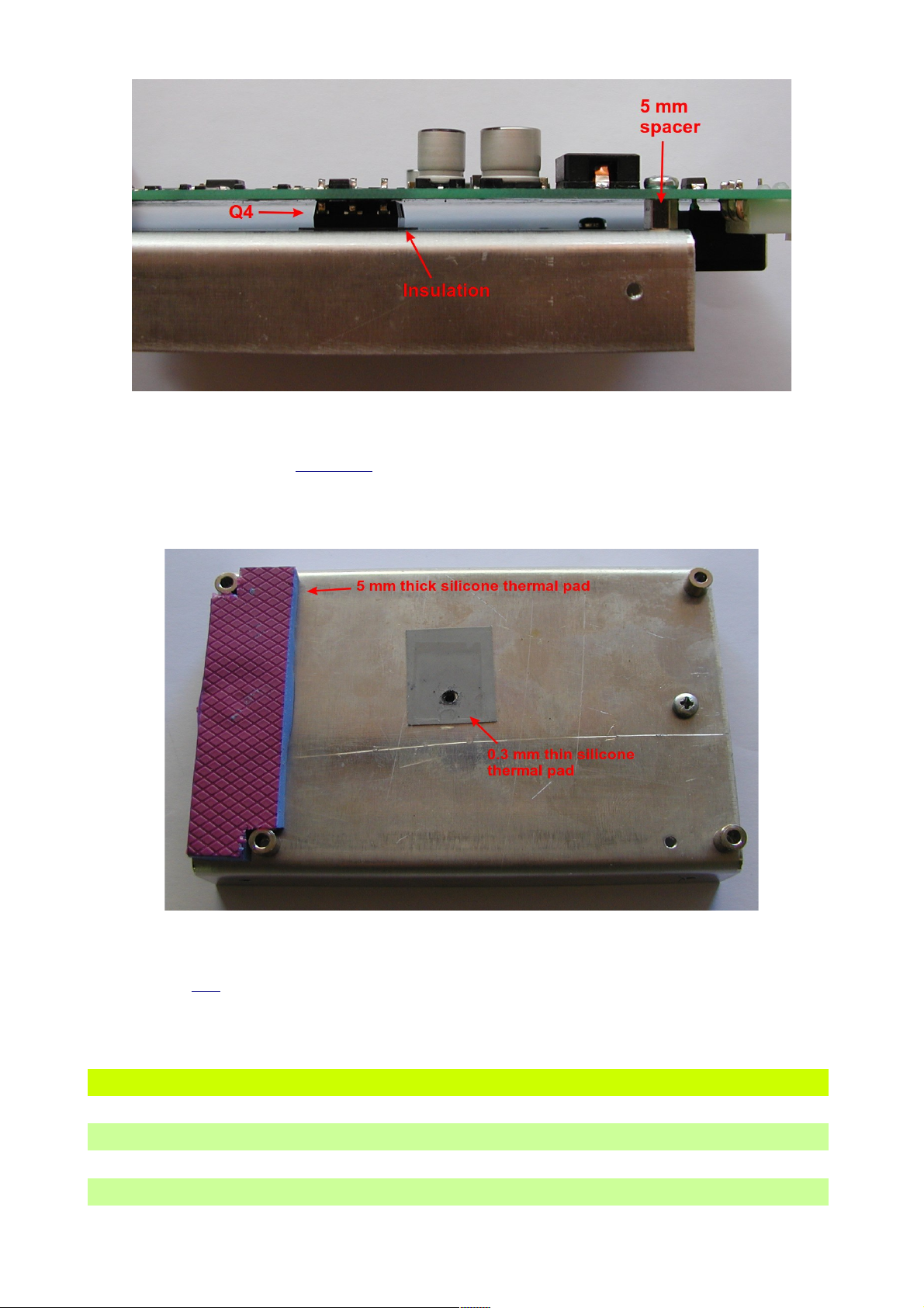
The Q4 has to be mounted on PCB’s bottom layer, and if EEZ H24005 customized enclosure is used,
please ensure that distance between its surface area and PCB bottom side is 5 mm The easiest way to
accomplish that is to mount PCB on the heatsink (Fig 22) using spacers, then mount Q4 (do not forget
insulation!), fix it with M3 screw and then start with its soldering
14
Fig 20: PWRGOOD signal transition (Power off)
Fig 21: Q4 preparation for mounting
EEZ PSU H24005 building instructions (r5B9)
It is highly recommended that below power pre-regulator section a piece of 5 mm thick silicone thermal
pad is mounted (search e g AliExpress) Channel temperature that is measured with NTC1 can be low-
ered in that way significantly With e g 20 mm wide pad (Fig 23) it’s possible to achieve 6 oC tempera-
ture drop on the max load Lowering temperature will also affect cooling fan operation which will work
with lower speed and makes it quieter
Do not use conductive thermal pad (e g aluminium block with PCB side insulated) since it will drasti-
cally increase EMI!
When everything is mounted, you can check few points before connecting it with the Arduino Shield that
is required for controlling the Power board:
Signal Value location Comment
+VREF +2 5 V IC10 Define overall precision
+OUT around zero Pin 23-26, X3
CV_ACTIVE +5 1 V (logical high) R88/R92 CV mode active (if U_SERVO is negative)
CC_ACTIVE +0 6 V (logical low) R101/R104
15
Fig 22: PCB side view with Q4 mounted on heatsink
Fig 23: Silicone thermal pads

EEZ PSU H24005 building instructions (r5B9)
POST_OE +4 67 V (logical high) R56 Output is disabled
U_SERVO -1 1 V D15 cathode
I_SERVO +0 28 V D17 cathode
Corrections
During the assembly and testing two issues are found on this board that will require PCB modifications
Fortunately both can be done without considerable effort or special skills The simpler one is related to
radiated EMI One of the PCB’s mounting holes is wired to the protective earth potential and the
mounted heatsink for the Q4 become also on that potential when it’s fixed on the PCB Our intention
was to attenuate EMI in that way, but the end results is quite contrary when the Power board is
mounted into metal (conductive) enclosure! It seems that in that way a whole enclosure is earthed not
on one but on three different point (one close to the AC inlet and two via above mentioned wiring of the
heatsink) and that generate ground loops
If you are going to use metal enclosure, it is advisable to simply cut the earth trace that leads to the
mounting hole which is near L2 power inductor as shown on Fig 24 Use miniature drill with a diamond
mill (example) for that
Another issue is connected with selection of the voltage programming source that in our case can be in-
ternal (DAC output, IC11) or external signal input (+2 5 V full scale) available via miniature push-in con-
nectors located on the Arduino Shield (X12, X14) Due to the mistake on PCB layout only internal pro-
gramming (that is default) is possible To overcome this issue we need to cut U_SET_OUT trace that
goes to R52 and connect it to R81 (Fig 25)
16
Fig 24: Earth PCB trace cut

EEZ PSU H24005 building instructions (r5B9)
A thin wire (e g for wire wrap) about 5 mm long is needed to be soldered (Fig 26, pos A) and PCB
trace has to be cut (Fig 26, pos B)
2. Enclosure and wire harness
The next step when all PCB modules are assembled and tested should be wiring and placing it into en -
closure The customized metal enclosure manufactured by Varisom has the following elements (Fig
27):
•Top and bottom plate with ventilation holes
•Front panel for TFT touch-screen display, binding posts, push-in connectors, light pipes
(example) for LEDs, etc
•Rear panel for AC inlet, USB, Ethernet, cooling fan and AUX PS module mounting holes
•Two set of three U-shaped aluminium heatsink with Power module mounting holes
•Mounting rail for AC/DC power modules and
•Mounting rail for TFT touch-screen display (wasn’t shipped with prototype!)
17
Fig 25: Voltage programming selection schematic modification
Fig 26: Voltage programming PCB modification

EEZ PSU H24005 building instructions (r5B9)
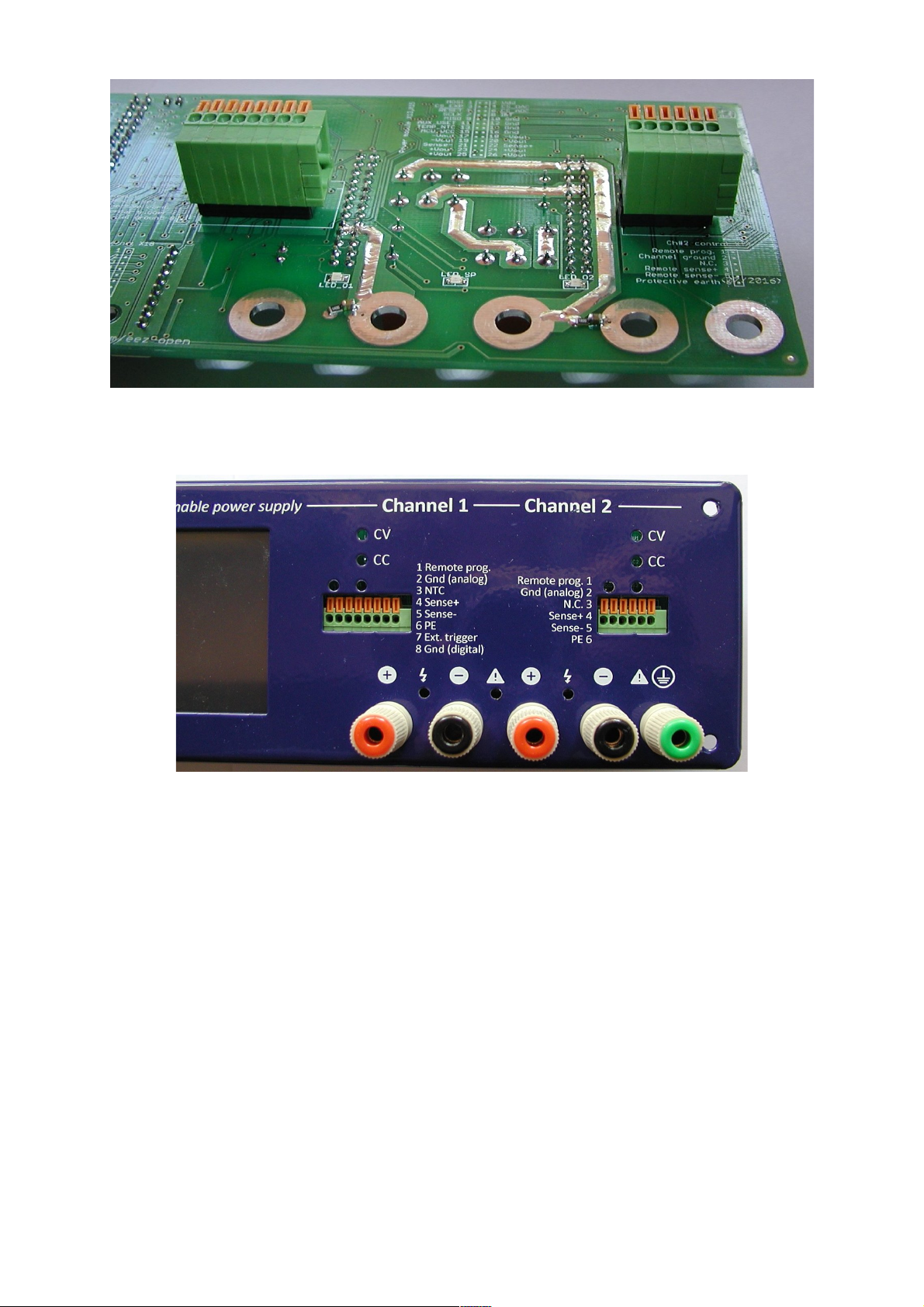
The Arduino Shield is mounted directly on the enclosure front panel and it’s fixed on nine positions: five
binding posts and four TFT touch-screen display spacers All LED indicators are mounted directly on
the PCB bottom layer a light pipes has to be added that their lights can be visible on the surface of the
front panel Since no separators between LEDs exists for better effect we masks each light pipe with
black heat shrink tube as shown in Fig 28
18
Fig 27: Customized metal enclosure
Fig 28: Front panel rear detail with masked light pipes and binding posts

EEZ PSU H24005 building instructions (r5B9)
Fig 29 shows block diagram that could help to get an idea how wiring looks like
The wire harness specification is available in separate section (link) that also include BOM Two cables,
one for USB connection between Arduino board and AUX PS module, and another IDC 10-pin flat cable
for powering Arduino shield are possible to get as already assembled All other cables has to be cut to
the size and equip with appropriate connectors Genuine crimping and wire cutting tools are expensive
and if you already don’t have them a fine alternative could be the following:
•Jokari No 20050
•Engineer Crimper with No 12 and No 13
Above mentioned specification is just an example how wire harness can be done, and one is free to use
wires of different type and length but with equal or bigger diameter and voltage rating for power paths
It’s also recommended to connect protective earth to the single point on the metal enclosure as shown
in Fig 30 Make sure that ring terminal has good electric contact with enclosure by using externally ser-
rated washer (example) Earthing requirement could vary from country to country therefore please
check what is applicable in your case
19
Fig 29: Block diagram

EEZ PSU H24005 building instructions (r5B9)
2.1. AC input selection
AC mains voltage defines what type of AC/DC modules or mains power transformer can be used for
powering the Power boards That also dictate fuse ratings and you can experiment with different fuse
types and ratings depends of selected AC/DC module or mains transformer In general the fuse current
rating has to be twice higher for 115 Vac then 230 Vac We are using 4 A (example) for two LRS-150-48
modules (max combined output power is 320 W and with listed 90 % power efficiency min 3 13 A is re-
quired) Two fuses are needed if AC IEC inlet such as Schurter 4304 6090 is used
20
Fig 30: Earth connection
Table of contents


.png)
.png)
.png)
.png)
.png)
.png)