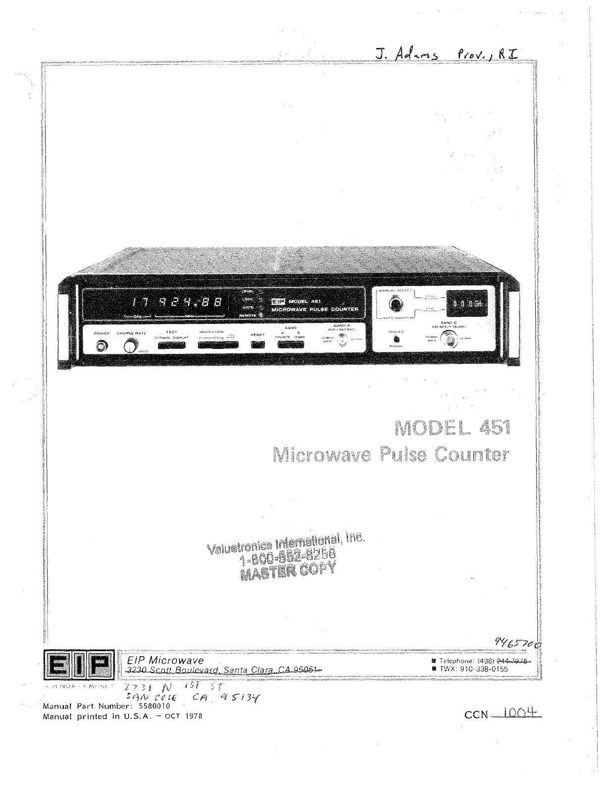
EIP 451 User manual
1
.
.
.
ure
P
ING1 MOLO.L. 451
1,mcfroyvmea PIA-5
71'6
6
P
,
1 .1tokApi
91
,
6.5
--,
e
(i'y
Telephone: ;=
j9I 1
7
.4
X :
910-338-0 I
Elf' Microwave
C
1
arq
-
CA
-
95064-
i
Manual Part Number: 5580010
Manual printed in U.S.A. — OCT 1978
CCN
Or)q-

MANUAL CHANGE INFORMATION
MODEL 451
At EIP we continually strive to keep up with the latest electronic developments by adding
circuit and component improvements to our instruments as soon as they are developed
and tested.
Sometimes, due to printing and shipment requirements, we cannot get these changes im-
mediately into printed manuals. As a result, your instrument may contain some or all of
the changes listed below.
PAGE NUMBER:
0-3.
A109
7,5K.
caler (5500079), Change R33 to 7,5K, 1/4 W.
Change R34 to 10K, 1/4 W.
.0-5.
A111 BCD Output/Remote Prog., Signal from P1 pin 15 to AS should be inhibit.
3-1.
Paragraph 3-8, line 4, should read "925 MHz - 18 GHz, or Band A (Option P2) for frequencies".
3-1.
Paragraph 3-15, last line should read "produce 1.5V at the INPUT INHIBIT thus enabling the 451".
8-7.
Al Basic Counter, Change FAN part number to 5000151.
8-7.
AMica.
ontrol (2020074), Change C5 to Mica, 200 pF, part number 2250009.
Add CR18, General Purpose diode, part number 2704154.
Delete R20.
8-8, A107 Power Supply (2020077), Change Cl to part number 2200016.
Change C5 to part number 2200018.
A106 High Frequency (2020081), Change R47 to part number 4130999.
8-9.
A107 Power Supply (2020077) Change R20 to part number 4130999.
8-9
A109 Prescaler (2020079) Change R33 to 4130752.
Change R34 to 4010103.
9-5.
A100, (5500070) Rear panel MIN PRF switch should be labeled 0 (not ON) and 50 Hz (not OFF). The blue
and green wires from J1 should be transposed so the green wire goes to 0.
9-9.
A103 Cou
U17.
hain schematic (5500083-A) U16, U17, and U18 - change pin 14 to pin 1.
9-13. A104 Control (5500074-0), Change C5
to 200
pF.
Replace R20 with CR18 (anode side to ground).
C2 should.be 6.3
V.
9-15.
A105 Gate Generator, Signal from P1M
to.
U14C pin 2 should be clo
(5500077).
.
9-19. A107 Power Supply (5500077), Change Cl value to 9500 uF .25V.
Change C5 value to 44,000 uF .15V.
Change 1920 to 5.6K, 2%.
9-33, A203 Converter Sequencer schematic - delete line between U7 pin 3 and U9 pin 2.
-add line bet
03.n U9 pin 2 and U4 pin 1.
-change 03, now shown as NPN, should be PNP,
-change C4 to .005 value.
4-1,
Paragraph 4-4, line 6 should read " 100us (or 1 ms)."
8-12. A204 IF Processor (2020094) - Note the following part number changes.
C25 is 2150003 R41 is 4130151
C33 is 2150003 R43 is 4130431
R32 is •4130431
R44 is 4130221
R34
is 4130271
R76 is 4130471
R35 is 4130221
.1
and make the following changes to your
R41 is now 150 ohm, 2%
R43 is now 270 ohm, 2%
R44 is now 220 ohm, 2%
R76 is now 470 ohm, 2%
9-35. A204 IF Processor (5500094) - Change the revision letter to
schematic diagram.
C25 is now .01µF
C33 is now .01µF
R33 is now 430 ohm. 2%
R34 is now 270 ohm. 2%
R35 is now 220 ohm. 2%
1-2. Table 1-1, Specifications
,
General. Gate error (max) should read "± 1§),014-1z." for Band A and "± 40kHz" for Band B.
PIN - .03
- .03
6-5. Paragraph 6-21, item b., (3) should read "'Adjust A106R60 per paragraph 6-21a (2)."
7-1. Paragraph 7-10, C. (b), last sentence should read "For 100 ns wide pulses. error should be less than 1.42 MHz,
7-2. Paragraph 7-10. 0 (51, last sentence should read "For 100 ns wide pulses, error should be less than 1.42 MHz.
Paragraph 7-11, C, add the following sentence, "Gate error should be less than 570 kHz.
9-5, A100 Counter Interconnect (5500070) - Delete Gate Mod switch that was connected to J1 pin 1 and 2 on the rear panel.
Delete modulation trace that runs from J1 pin 1 to High Frequency XA106 Pin 15,
9-15. A105 Gate Generator, J1 should read BAND B THRESHOLD and J2 should read BAND A THRESHOLD.
9-17. A106 High Frequency, R47 should be 18 ohm nom.,
2%, S.A.T.
9-29, A202 YIG Control, Add US Inverter Gate , pin 11 (in)/10(out) from P1 pin 7, 40 kHz Clock signal to
U4 pin 14,
EFIROR DAC ENABLE, at U6 pin 2 should be ERROR DAC ENABLE.
ERROR DAC STJ
-
P
-
,at U6 pin 11 should be ERROR DAC STEP.
CERTIFICATION
EIP Microwave certifies that this instrument was throroughly inspected and
tested, and found to be in conformance with the specifications noted herein
at time of shipment from factory .
WARRANTY
EIP Microwave warrants this counter to be free from defects in material and
workmanship for one year from the date of delivery. Damage due to accident,
abuse, or improper signal level, is not covered by the warranty. Removal,
defacement, or alteration, of any serial or inspection label, marking, or seal,
may void the warranty. EIP Microwave will repair or replace at its option,
any components of this counter which prove to be defective during the warranty
period, provided the entire counter is returned PREPAID to EIP or its authorized
service facility. In-warranty counters will be returned freight prepaid; out-of-
warranty units will be returned freight COLLECT . No other warranty other than
the above warranty is expressed or implied.
ASSISTANCE
For assistance, contact the EIP representative in your area, or EIP Microwave.
iii

TABLE OF CONTENTS
PARA-
GRAPH
TITLE
PAGE
SECTION 1 - GENERAL INFORMATION AND SPECIFICATIONS
1-1
Description
1-1
1-9
Instrument Identification
1-i
1-11
Specifications
1-1
SECTION 2 -- INSTALLATION
2-1
Unpacking
2-1
2-4
Installation
2-1
2-6
Incoming Operational Check
2-1.
SECTION 3 - OPERATION
3-1
Introduction
3-1
3-3
Controls, Indicators and Connectors
3-1
3-5
Numerical Display Brightness Adjustment
3-1
3-7
Operation in the Automatic Mode
3-1
3-10
Operation in the Manual_ Mode
3-1
3-12
Externally Enabled Operation
3-1
3-14
Input inhibit Requirements
3-1
3-16
Pulse Profile Measurements
3-1
3-18
Dynamic Characteristics of Time Varying Signals
3-4
3-20
Multiple Pulse Signal Measurements
3-4
3-22
Timing Considerations
3-4
3-24
Accuracy
3-5
3-23
Time Base Errors
3-5
3-31
Averaging Error
3-5
3-33
Gate Error
3-6
3-35
Techniques For Improving Accuracy
3-6
3-37
Time Base Calibration
3-6
3-39
Long Term Averaging
3-6
3-41
Gate Error
3-6
SECTION 4 - GENERAL THEORY OF OPERATION
4-1
General
4-1
4-8
Microwave Converter
4-1
4-18
350 MHz Direct Counter
4-3
4-23
Gate Generator
4-4
4-27
Accuracy
4-4
An Introduction to YIG Filters
4-5
SECTION 5 - MAINTENANCE & SERVICE
5-1
General
5-1
5-3
Fuse Replacement
5-1
5-5
Air Circulation
5-1
5-7
Counter Servicing
5-1
5-8
Recommended Service Procedure
5-1
5-9
Servicing Precautions
5-I
.
5-10
Factory Service
5-1
5-12
TROUBLESHOOTING
5-2
5-13
Malfunction at Turn-On
5-2
5-15
Failure to Indicate All Zeros
5-2
5-17
Malfunction in Self Test
5-2
iv

TABLE OF CONTENTS (Continued
PARA-
GRAPH
TITLE
PAGE
SECTION 5 (CONTINUED)
5-19
Malfunction in Band A (Option P2)
5-2
5-21
Malfunction in Band B
5-2
5-23
Module Failure Verification
5
-
3
5-24
Source/Amplifier Power Output Check
5-3
5-25
Source/Amplifier. Spurious Signal Check
5-3
5-26
Front End Check
9-3
5-27
Mixer Check
5-3
5-28
PIN
Limiter/Attenuator Check
5-3
5-29
YIG Comb Generator Check
5-4
5-30
IF Processor Check
5-5
SECTION 6
-
ADJUSTMENTS & CALIBRATION
General
6-1
6-3
Generating and Measuring Narrow RF Pulses
6-1
6-8
Power Supply Adjustment
6
-
3.
6-10
Time Base Calibration
6
-
1.
6-12
RTO Calibration Procedure
6-3
6-13
TeX() Calibration (Option P1)
6-3
6-18
TCXO Calibration Procedure
6
-
3
6-19
Band A (Option P2) Adjustments
6-3
6-20
Band B Adjustments
6
-
3
6-21
High Frequency (A106) Adjustment
6-5
SECTION 7 - PERFORMANCE TESTS
7-1
General
7
-
1
7-3
Variable Line Voltage
7-1
7-5
Recommended Test Equipment
7-1
7-7
PERFORMANCE TESTS
7
-
1
7-8
Range, Sensitivity, and Minimum Pulse Width - Band A (Option P2)
7
-
1
7-9
Range, Sensitivity, and Minimum Pulse Width - Band B
7-1
7-10
Gate Error - Band A (Option P2)
7-1
7-11
Gate Error - Band B
7-2
7-12
Rear Panel Output Levels
7-2
7-13
Rear Panel Input Inhibit Levels
7-2
SECTION 8 - PARTS LISTS
8-1
General
8-1
8-3
List of Tables
8-1
8-4
To Order Replacement Parts
8-1
SECTION 9
-
CIRCUIT SCHEMATICS S DESCRIPTIONS
-
COMPONENT LOCATORS
9
-
1
General
9
-
1
SECTION 0
-
OPTIONS
0-2
Option P1 - TCXO
0-1
0-4
Option P2 - Prescaler
0-1
0-6
Option P3 - Rear Panel Inputs
0-1
0-8
To Field Change Band B to Rear Input
0
-
1
0-9
To Field Change Bands A and B to Rear Input
0-1
0-10
Option P4 BCD Output/Remote Programming
0-1
0-12
BCD Outputs
0-1
0-15
YIG Preset
0-1
0-17
Remote Programming
0-1
LIST OF TABLES
TABLE
TITLE
PAGE
1-i,
Specifications
1-2
3-1
Front Panel Controls, indicators and Connectors
3-2
3-2
Rear Panel Controls and Connectors
3-3
5-1
Recommended Test Equipment
5-4
8-1
Reference Designators and Abbreviations
8-1
8-2
List of Manufacturers
8-2
8-3
Master Parts List
8-3
8
-
4
Replaceable Parts List
8-7
9
-
6A
Control Sequence
9-11
9-15A
Converter Sequence Functions
9-31
0-1
Pin Assignments - BCD Output/Remote Programming (Option P4)
0-4
vi
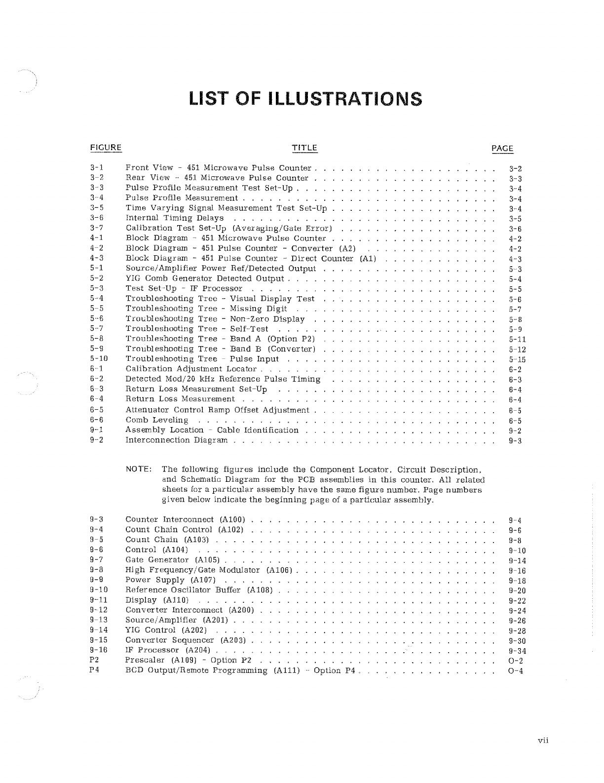
LIST OF ILLUSTRATIONS
FIGURE
TITLE
PAGE
3-1
Front View - 451 Microwave Pulse Counter
3-2
3-2
Rear View -- 451 Microwave Pulse Counter
3
-
3
3-3
Pulse Profile Measurement Test Set-Up
3-4
3-4
Pulse Profile Measurement
3-4
3-5
Time Varying Signal Measurement Test Set-Up
3-4
3
-
6
Internal Timing Delays
3-5
3-7
Calibration Test Set-Up (Averaging/Gate Error)
3-6
4-1
Block Diagram - 451 Microwave Pulse Counter
4
-
2
4-2
Block Diagram - 451 Pulse Counter - Converter (A2)
4-2
4-3
Block Diagram - 451 Pulse Counter - Direct Counter (A1)
4-3
5-1
Source/Amplifier Power Ref/Detected Output
5
-
3
5-2
YIG Comb Generator Detected Output
5-4
5
-
3
Test Set-Up - IF Processor
5-5
5-4
Troubleshooting Tree - Visual Display Test
5-6
5-5
Troubleshooting Tree - Missing Digit
5-7
5-6
Troubleshooting Tree - Non-Zero Display
5
-
8
5-7
Troubleshooting Tree - Self-Test
5-9
5-8
Troubleshooting Tree - Band A (Option P2)
5
-
11
5-9
Troubleshooting Tree - Band B (Converter)
5-12
5-10
Troubleshooting Tree - Pulse Input
5-15
6-1
Calibration Adjustment Locator
6-2
6-2
Detected Mod/20 kHz Reference Pulse Timing
6-3
6-3
Return Loss Measurement Set-Up
6-4
6-4
Return Loss Measurement
6-4
6
-
5
Attenuator Control, Ramp Offset Adjustment
6
-
5
6-6
Comb Leveling
6-5
9-1
Assembly Location - Cable Identification
9-2
9-2
Interconnection Diagram
9-3
NOTE: The following figures include the Component Locator, Circuit Description,
and Schematic Diagram for the PCB assemblies in this counter. All related
sheets for a particular assembly have the same figure number. Page numbers
given below indicate the beginning page of a particular assembly.
9-3
Counter Interconnect (A100)
9-4
9-4
Count Chain Control (A102)
9-6
9-5
Count Chain (A103)
9
-
8
9-6
Control (A104)
9-10
9-7
Gate Generator (A105)
9-14
9-8
High Frequency/Gate Modulator (A106)
9-16
9-9
Power Supply (A107)
9-18
9-10
Reference Oscillator Buffer (A108)
9-20
9-11
Display (A110)
9-22
9-12
Converter Interconnect (A200)
9-24
9-13
Source/Amplifier (A201)
9-26
9-14
YIG Control (A202)
9-28
9-15
Converter Sequencer (A203)
9-30
9-16
IF Processor (A204)
9-34
P2
Prescaler (A109) - Option P2
0-2
P4
BCD Output/Remote Programming (A111) Option P4
0-4
vli

SECTION 1
GENERAL INFORMATION & SPECIFICATIONS
1-1. DESCRIPTION
1-2, The MP Model 451. Microwave Pulse Counter auto-
matically and directly measures the frequency of pulse
modulated microwave signals between 300 MHz - 18 GHz.
Pulse widths can be as narrow as 100 nanoseconds, with
no minimum or maximum pulse repetition frequency limits.
1-3. The 451 also measures the frequency of CW micro-
wave signals. and carrier signals with FM modulation up
to 40 MHz peak-to-peak deviation at 10 MHz modulation
rates. No manual switching is required to measure CW or
pulsed frequencies — the counter will automatically mea-
sure either type of signal. Sensitivity is -10 dBm
,
to 10
GHz; -5 dBm to 18 GHz. A built-in limiter provides over-
load protection of up to 1 watt peak from 925 MHz - 18 GHz.
1
-
4. All front panel controls except SAMPLE RATE are
externally programmable, One input to the counter (Band
B) accepts signals over the range of 925 MHz - 18 GI-1z,
Option P2 provides a second input (Band A) to cover the
range of 300 MHz - 950 MHz.
1-5. The display on the 451 Counter provides a direct
readout of the measured frequency over the entire oper-
ating range of the counter with 10 kHz resolution. The
counter also includes automatic suppression of leading
zeros, except during a no signal input condition.
1-6. The frequency readout of the 451 is displayed in a
fixed position format that is conveniently sectionalized in
GHz and MHz. Gate times are 100 us and 1 ms.
1-7. For applications where less resolution is required,
pushbutton display blanking (RESOLUTION) is provided
to simplify the readout.
1-8. To assure trouble-free performance, the 451 Pulse
Counter is completely solid-state. For ease of repair and
maintenance, the major portion of the counter circuitry is
contained on plug-in printed circuit boards or in easily
removed modules. Special test points allow monitoring of
critical circuit functions,
1-9. INSTRUMENT IDENTIFICATION
1-10. The 451 Pulse Counter is identified by two number
sets: the Model and Configuration Control Number (e .g:
451
-
CCN1001), and a specific Serial Number (e.g: 12345).
Both sets of numbers should be mentioned in any corre-
spondence or parts orders relating to the counter,
1-11. SPECIFICATIONS
1-12. Model 451 Microwave Pulse Counter specifications
are given in Table 1-1,
1-1
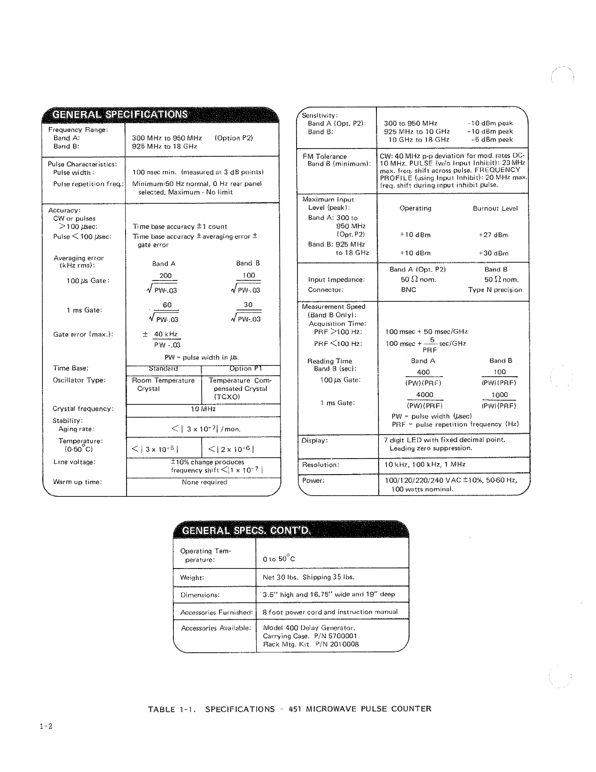
GENERAL SPECS,
coNro
0 to 50
°
C
Net 30 lbs. Shipping 35 lbs.
Weight:
Dimensions:
3.5" high and 16.75" wide and 19" deep
Accessories Furnished:
8 foot power cord and instruction manual
I
,
„...., ...„
Accessories Available:
Model 400 Delay Generator.
Carrying Case. P/N 5700001
Rack Mtg. Ka. P/N 2010008
TABLE 1-1. SPECIFICATIONS - 451 MICROWAVE PULSE COUNTER
GENERAL SPECIFICATIONS.
Frequency Range:
Band A:
Band B:
300 MHz to 950 MHz
(Option P2)
925 MHz to 18 GHz
Pulse Characteristics:
Pulse width:
Pulse repetition freq.:
100 nsec mm. (measured at 3 dB points)
Minimum-50 Hz normal, 0 Hz rear panel
selected, Maximum - No limit
Accuracy:
CW or pulses
>100 bisec:
Pulse <100 psec:
Averaging error
(kHz rmsl:
100 gs Gate:
1 ms Gate:
Gate error (max.):
Time Base:
Oscillator Type:
Crystal frequency:
Stability:
Aging rate:
Temperature:
(0-50 C)
Line voltage:
Warm up time:
\---
Time base accuracy ±1 count
Time base accuracy ± averaging error ±
gate error
Band A
selected.
100
ni
200
PW-.03
VPW-.03
. _
60
30
Al PW-.03
±
40 kHz
Ai PW-.03
width in /15.
PW -.03
PW - pulse
Standard
Option P1
Room Temperature
Crystal
Temperature Corn-
pensated Crystal
(TCX0)
10 MHz
< I 3 x 10
-7
1 /mon.
<I 3 x10
-5
1
<1 2 x 10
-6
1
±10% change produces
frequency shift <VI x 10
-7
1
None required
Sensitivity:
Band A (Opt. P2):
Band B:
300
to 950 MHz
-10 dBm peak
925 MHz to 10 GHz
-10 dBm peak
10 GHz to 18 GHz
-5 dBm peak
FM Tolerance
Band B (minimum):
CW: 40 MHz p-p deviation for mod. rates DC-
10 MHz. PULSE (w/o Input Inhibit): 20MHz
max. freq. shift across pulse. FREO.UENCY
PROFILE (using input Inhibit): 20 MHz max.
freq. shift during input inhibit pulse.
Ma
ximum Input
Level (peak):
Band A: 300 to
950 MHz
(Opt.P2)
Band B: 925 MHz
to 18 GHz
Operating
Burnout Level
+10 dBm
+27 dBm
+10 dBm
+30
dBm
Input Impedance:
Connector:
Band A (Opt. P2)
Band B
50
2
nom.
50
2
nom.
BNC
Type N precision
Measurement Speed
(Band B Only):
Acquisition Time:
PRE >100 Hz:
PRF <100 Hz:
Reading Time
Band B (sec):
100
ps
Gate:
1 ms Gate:
100 msec + 50 msec/GHz
100 msec + —
5
sec/GHz
PRF
Band A
Band B
400
100
(PW)(PRF)
(PWI(PRF)
4000
1000
(PW)(PRF)
IPW)(PRF)
PW
-.
pulse width (11sec)
PRF --- pulse repetition frequency (Hz)
Display:
7 digit LED with fixed decimal point.
Leading zero suppression.
Resolution:
10 kHz, 100 kHz, 1 MHz
Power:
100/120/220/240 VAC ±10%, 50-60 Hz,
100 watts nominal.
1-2

FRONT PANEL
Controls:
Sample Rate/Hold:
Test-200 MHz:
Display Test:
Resolution:
1 ms Gate:
Band Select (A or 13):
Varies display reading time from 0.1 sec/
reading to 10 sec/reading. "Hold" displays
last reading.
Displays 200 MHz internal test frequency.
Tests all LED numeral se
position.
(1 MHz, 100 kHz, 10 kHz):
Sets display
resolution.
Selects 1 ms gate.
Switch selects either Band A (Opt. P2) or
Band B input.
Auto/Manual (Band B):
Auto Mode:
Manual Mode:
Band B searches upward for input signal be-
ginning 100 MHz above preset number.
Inhibits search.
Signal must lie between
100 MHz and 325 MHz above preset
number.
Thumbwheel Switch
(Band B):
Auto
inhibit.
Manual Mode:
Sets start point of frequency sweep (100
MHz above preset number.)
Sets operating frequency range (100 MHz
to 325 MHz above preset number.)
Indicators:
LeveI:
Lock:
Gate:
Remote:
Reduce Signal
(Band B):
Indicates
sufficient input level.
Indicates signal acquired.
Indicates
measurement in process.
Indicates Remote Programming (Option
P4
Or
PS)
active.
Indicates excess signal level.
Connectors:
Band A input:
BkHz.
B input:
Type BNC female - 300 to 950 MHz
(Option P2)
Type N precision female - 925 MHz to
18 GHz
Controls:
Power input:
Power module containing AC connector,
fuse, and voltage control for 100, 120,
220, or 240 VAC.
Storage (On/Off):
Normally on. In off position,
display up-
dates
continuously during measurement
cycle.
Min. PRF = (50 Hz/
0):
Normally
in
50 Hz position. In 0 position,
allows measurements of very low
PRF
signal.
Connectors:
10 MHz reference
output:
1 V peak-to-peak min. into 50
2
Gate Output:
-0.5v min. into 50
2
corresponding to
counter gate.
Signal Threshold
Output:
-0.5v min. into 50
2
corresponding to
signal exceeding threshold.
Inhibit Input:
ECL high (-0.9v) inhibits. ECL low (-1.7v)
enables. From
50 CZ
source, 0 volts will
inhibit,
-
1v
will enable.
Input impedance: 50
2to -2 volts.
MODEL / OPTIONS:
Model 451
Microwave Pulse Counter
P1:
TCXO - temperature compensated crystal
oscillator
P2:
Band
A:
300 -
950
MHz
P3:
Rear panel inputs: Band A and B
P4:
BCD output/remote programming
Remote programming: provides rear
panel programming of all front panel
controls except SAMPLE RATE.
Requires ground contact closure; one
control line per function (T
2
L and DTL
compatible).
Digital output:
7 data digits in parallel
form. 1-2-4-8 "1" state positive.
P5
GPIB: System interface per IEEE STD
488-1975.
----)
TABLE 1
-
1 (Continued) SPECIFICATIONS
-
451 MICROWAVE PULSE COUNTER
1-3

SECTION 2
INSTALLATION
2-1. UNPACKING
2-2. The EIP Model 451 Microwave Pulse Counter arrives
ready for operation. Carefully inspect the shipping carton
before opening for any evidence of visible or concealed
damage. If any seems apparent, ask that the shipper's
agent be present when the counter is unpacked.
2-3. Remove the packing carton and supports, being
careful not to scar or damage the counter. Make a com-
plete visual inspection of the counter. checking for any
damage or missing components. Check that all switches
and controls operate mechanically. Report any damage
to EIP immediately.
2-4. INSTALLATION
2-5. There are no special installation instructions for
the 451 Pulse Counter. The unit is
a
self-contained bench
or rack mounted instrument. which only requires connec-
tion to a standard, single-phase, 100/120 or 220/240 volt,
50-60 Hz power line for operation. CAUTION: Check cur-
rent rating of counter fuse and voltage range PC board in
power module (on rear panel of counter) before applying
power to the counter, Module PC board should show the
correct nominal line voltage when installed in the module.
2-6. INCOMING OPERATIONAL CHECK
2-7. The following procedure outlines an operational
check of the counter which may be conducted without
special tools. signal generators, or test equipment. The
internal Time Base Clock is used as the input signal to
the Direct Counter, therefore it cannot check the opera-
tion of the Band A Prescaler or the Band B Converter.
a. Turn counter POWER switch off. Check fuse rat-
ing and card in power module (see paragraph 2-5),
b.
Connect counter power cord to the voltage source
specified in paragraph 2-5. The ground terminal on
the power cord plug should connect to a reliable earth
ground.
c.
Press POWER switch (on front panel) to turn
counter on. The counter display should light, and the
internal cooling fan should operate.
d.
Partially depress either of the two RESOLUTION
switches and release it. so neither switch remains in
the depressed position. All digits in the display should
indicate "0" (zero).
e.
Depress the front panel 200 MHz TEST switch. The
display should indicate "200.00" (200 MHz). Note that
the two leading zeros are blanked (not lit).
f.
Blank the 10 kHz digit by pressing the right hand
RESOLUTION switch.
g.
Depress the 200 MHz TEST button again. The dis-
play should indicate "200,0".
h.
Test both RESOLUTION switches. Note that the dig-
it immediately above the switch, and any digit to the
right will be blanked.
i.
Unblank all display digits (see "d" above).
j.
With no input signal, the entire display should show
all zeros in both positions of the BAND switch.
k.
Depress the DISPLAY TEST switch. All display dig-
its should show "8" (all segments of each digit lighted).
1. This completes the counter operational check.
SECTION 3
OPERATION
WARNING
DO NOT APPLY A SIGNAL EXCEEDING
THE MAXIMUM INPUT SPECIFICATION
TO ANY INPUT. EXTENSIVE DAMAGE
NOT COVERED BY THE WARRANTY
WILL OCCUR, EVEN IF THE COUNTER
IS TURNED OFF, OR APPEARS TO BE
INOPERATIVE.
3-1. INTRODUCTION
3
-
2.
The Model 451 Microwave Pulse Counter has three
principle modes of operation: automatic, manual, and ex-
ternally enabled. This section will describe each of these
modes, and will provide information
on
timing considera-
tions and instrument accuracy.
3
-
3.
CONTROLS, INDICATORS AND CONNECTORS
3-4. Front panel controls, indicators and connectors are
shown in Figure 3-1 and described in Table 3-1, Rear
panel controls and connectors are shown in Figure 3-2
and described in Table 3-2,
3
-
5.
NUMERICAL. DISPLAY BRIGHTNESS ADJUSTMENT
3
-
6. Apparent brightness of the light-emitting-diode
(LED) numerical display may be varied by adjustment of
potentiometer A102R35. (R35 is located near the top front
of PC Board A102, and is accessible by removing the top
cover of the counter.) Adjust R35 clockwise to increase
display brightness, or counter-clockwise to decrease the
brightness.
3
-
7. OPERATION IN THE AUTOMATIC MODE
3
-
8.
In this operational mode, either CW or pulse signals
can be measured. Connect the input frequency to the ap-
propriate input connector:
Band B
for frequencies between
825 MHz - 18 GHz. or Band A (Option Pa) for frequencies
between 300 MHz - 950 MHz. If the input signal level is
sufficient for counting, the
LEVEL
indicator will light. If
the proper band and input have been selected, the
LOCK
indicator will light. In Band B, if the input signal_ level is
too high. the
REDUCE SIGNAL
indicator will light. Meas-
urements will be made at a rate determined by the
SAM-
PLE RATE
control.
3-9. In Band B, acquisition speed may be improved by
presetting the start frequency via the thumbwheel switch.
The minimum frequency which can be acquired will then
be 100 MHz above the switch setting.
CAUTION: An erroneous reading may result if an applied
signal is less than 700 MHz above the switch setting.
3-10. OPERATION IN THE MANUAL MODE
3-11. Manual mode operation applies to Band B only,
and is achieved by setting the
MANUAL SELECT/AUTO
SWEEP
switch to the
MANUAL SELECT
position, and the
thumbwheel switch to the proper frequency. In this mode.
the operating frequency range is from 100 MHz to 325 MHz
above the switch setting. Since no sweep is required, the
acquisition time in this mode is virtually eliminated,
CAUTION: Application of signals which lie between 100 -
325 MHz below the switch setting may result in erroneous
readings.
3-12. EXTERNALLY ENABLED OPERATION
3
-
13. The use of the rear panel
INPUT INHIBIT
makes
possible a class of measurements known as
dynamic
frequency measurements
—
measurements made at a
specified point in time on a signal whose frequency is
some repetitive function of time. When a high level is
applied. the 451 is inhibited from making a measurement.
Thus a signal at the
INPUT INHIBIT
can be used as an en-
able signal to make a measurement at a desired time. The
width of the enable signal determines the duration of the
measurement — typically 40 nanoseconds less than the ap-
plied pulse.
3
-
14. INPUT INHIBIT REQUIREMENTS
3-15. The
INPUT INHIBIT
on the 451 is designed to be
compatible with either a 50 ohm impedance pulse genera-
tor. or emitter-coupled-logic (ECL) devices. An internal
termination of 50 ohms returned to -2 volts makes this
dual compatibility possible. An ECL high level signal
(
-
0.8 to -1,1 V) will inhibit measurement, while an ECL
low level signal (-1.5 to -2.0 V) will enable measurement.
ECL devices are designed to drive 50 ohm lines without
reflections when the lines are terminated with 50 ohms re-
turned to -2 V. The direct compatibility with a 50 ohm
pulse generator results from the fact that zero volts from
a 50 ohm source will produce -1 V at the
INPUT INHIBIT
.
(inhibiting the 451), while a -1 V signal into 50 ohms will
produce 4'V
at
the
INPUT INHIBIT
thus enabling the 451.
3
-
16. PULSE PROFILE MEASUREMENTS
3-17. Automatic pulse measurements can determine the
average frequency of a pulse. In some cases however,
additional information may be necessary. For example. a
pulsed magnetron may exhibit substantial frequency shift
(Continued on Page 3-4)
3-1
LiP
"QaE4-
CONTROLS.
faiRwAv.E. ovt.sE
:couNTER
f
'
FIGURE 3-1. FRONT VIEW - 451 MICROWAVE PULSE COUNTER
TABLE 3-1, FRONT PANEL CONTROLS, INDICATORS AND CONNECTORS
POWER On/Off Switch
Turns counter power on and off.
SAMPLE RATE/HOLD Control
Continuously variable control for one-tenth to ten seconds
per reading. (Required Gate time is added to sample time.)
HOLD position retains reading until manually reset.
200 MHz TEST Switch
Provides check of internal counter circuits. Display should
indicate "200.00 MHz.
DISPLAY TEST Switch
Displays "88 888.88
1
to test all LED segments.
RESOLUTION (100 is GATE) Switches
Provide blanking of either one or two least significant
digits for resolution of 10 kHz, 100 kHz, or 1 MHz, with
100 microsecond gate time.
I ms GATE Switch
Provides 10 kHz resolution with 1 millisecond gate time
for reduced pulse averaging error.
RESET Switch
Manually overrides the SAMPLE RATE/HOLD control,
resets display to zero, and initiates a new reading.
BAND Select Switches
Select desired operating band — either BAND A (Option
P2 - 300 MHz to 950 MHz). or BAND B (900 MHz to 18 GHz).
BAND A Connector
BNC female connector for Band A input (Option P2).
Visual Display
The 7-digit LED (light-emitting-diode) display provides
a direct numerical readout of the input frequency. The
display is sectionalized into GHz and MHz ranges.
LEVEL Indicator
When lit, indicates that input signal is of sufficient level
for counting. Blinking light indicates that PRE (pulse re-
petition frequency) is too low.
LOCK Indicator
When lit, indicates that input signal has been acquired.
GATE Indicator
Indicates that counter is in measurement portion of its
cycle.
REMOTE Indicator
Used with Option P4 (BCD/Remote Programming). When
lit, indicates that Remote Enable has been activated, and
that all front panel controls except SAMPLE RATE are
disabled.
MANUAL SELECT/AUTO SWEEP Switch
Selects manual or automatic operation for Band B.
PRESET/START FREQUENCY Thumbwheel Switch
In the MANUAL mode, the switch sets the operating fre-
quency range. The signal must lie between 100 MHz to
350 MHz above switch setting. In the AUTOMATIC mode,
the switch sets the start of the search range. Input fre-
quency must be at least 100 MHz above switch setting.
REDUCE SIGNAL Indicator
Indicates excessive signal input to Band B. WARNING:
Signals in excess of rated specifications may cause ex-
tensive damage NOT covered by the warranty.
BAND B Connector
Type N precision connector for Band B operation.
3-2

FIGURE 3-2. REAR VIEW - 451 MICROWAVE PULSE COUNTER
TABLE 3-2. REAR PANEL CONTROLS AND CONNECTORS
Rear Panel Inputs
(Option
P3) Allows modification of counter for rear panel
inputs.
ACCESSORY POWER OUT Connector
Provides power for 451 Pulse Counter accessories.
10 MHz OUTPUT Connector
Output of internal 10 MHz clock. 1 V p
-
p min into 50 ohms.
SIGNAL THRESHOLD OUTPUT Connector
Pulse output representing signal threshold level of input
pulse. Typically occurs 20 nanoseconds after
input
pulse,
and is used for frequency profile measurements.
GATE OUTPUT Connector
Provides Gate pulse representing actual time at which
measurement is being made. Used in frequency profile
measurement.
INPUT INHIBIT Connector
External pulse input for frequency profile measurements.
Remote Input/Output Connector
(Option P4) Connector for BCD/Remote Programming.
GPIB Input/Output Connector
(Option P5) For connection to General Purpose Interface
Bus (IEEE STD 488-1975). Refer to separate Instruction
Manual for EIP Model 451 Option P5.
STORAGE Switch
Normally ON. In the OFF position, display updates con-
tinuously
during measurement cycle.
MIN PRE Switch
Normally
in 50 Hz position. In 0 position, allows meas-
urement of very low PRE signal. NOTE: Reading
will
not automatically reset when signal is removed.
AC Power Module
Contains AC power line
receptacle, fuse. and PC board
for voltage selection.

1
1
INPUT SIGNAL 300 N11-1.,
GFI
z
FREGUENCY PROFILE
AVERAGE
PROFILE
-
MEASURE
ENT WINDOW
•
•
•
•
• • •
NHIBIT
II
NPUT
MODULATOR
451
MICROWAVE
PULSE
COUNTER
DELAYING
PULSE
GENERATOR
PULSE
OUTPUT
MODULATED
MICROWAVE RE
OUTPUT
INPUT
SOURCE
TO BE
TESTED
II
FREQUENCY
MODULATION
f INPUT
MODULATION
OUTPUT
TRIGGER
_EL
INPUT
I
TRIGGER
OUTPUT
I
near the leading and trailing edges of the pulse, or
a
pulsed Gunn diode oscillator may exhibit frequency shift
during a pulse due to peak power thermal effects. Meas-
urements of these characteristics are easily made with
only the 451 and a delaying pulse generator (see Figure
3-3). The
SIGNAL THRESHOLD
output of the 451 is used
to trigger the pulse generator. The generator's output
pulse is used as an enable input to the 451. As the pulse
delay is varied, the measurement window can be "walked"
through the pulse. A plot of frequency-versus-delay
gives the frequency-versus--time profile of the pulse di-
rectly as shown in Figure 3-4. The width of the measure-
ment window is determined by the width of the pulse gen-
erator output. Measurement windows of 50 nanoseconds or
less can be used, although wider windows yield higher
accuracy.
SIGNAL
THRESHOL
451
MICROWAVE
INHIBIT
PULSE
COUNTER
INPUT
SIGNAL
INPUT
PULSE TRIGGER
OUTPUT INPUT
DELAYING
PULSE
GENERATOR
FIGURE 3-3.
PULSE PROFILE MEASUREMENT TEST SET-UP
FIGURE 3-4. PULSE PROFILE MEASUREMENT
3-18. DYNAMIC CHARACTERISTICS OF TIME VARYING
SIGNALS
3-19. Many complex signals are not pulses at all but
simply continuous signals whose frequency varies repeti-
tively with time. One example is the measurement of the
response of
a
device such as a voltage controlled oscil-
lator (VCO). A square wave applied to the tuning voltage
will produce a response curve of frequency-versus-time
allowing measurement of various settling times such as
post-tuning drift, Another possible application would be
the measurement of linearity and amplitude for frequency
modulated radar altimeter signals. Figure 3-5 shows
a
test set-up designed to make measurements on time vary-
ing signals. It is similar to the pulse profile test set-up,
except that in this case since
present.
always a signal
present, a trigger must be obtained from the modulating
source. This will trigger the pulse generator which con-
trols the measurement.
3-20. MULTIPLE PULSE SIGNAL MEASUREMENTS
3-21. Another type of measurement is that of a repetitive
sequence of pulses differing in frequency. In this case,
it is desirable to measure the frequency of each pulse in
the sequence separately. The same test set-up as shown
in Figure 3-5 is required, with the trigger pulse synchro-
nous with the sequence. In this measurement, the
INPUT
INHIBIT
is used simply to discriminate between pulses.
The enabling pulse can be slightly wider than the pulse
to be measured. The 451 will automatically restrict the
measurement window entirely within the pulse. By shift-
ing the delay time of
theenabling pulse, each input pulse
of the sequence can be separately measured.
FIGURE 3-5.
TIME VARYING SIGNAL MEASUREMENT TEST SET-UP
3-22. TIMING CONSIDERATIONS
3-23. Under most circumstances, internal timing within
the 451 would be of
no concern to the user. However, in
applications where a few nanoseconds are significant,
some details of internal operation are important. These
involve two areas: (a) measurement window width, and
(b) internal timing delays.
(a) Measurement Window Width
The measurement window is the period during which
the
GATE
is actually open to enable the counting of a
signal. This
GATE
width will typically be 30 nanosec-
onds narrower than the pulse applied to
the INPUT
3-4
INPUT MPCSOWAVE PULSE
I
-ulU
SIGMA PHRESNDLO
hi— -60ns
NHL
5- W.
t
ow
-30ns
DE
LAY ED iF
PULSE
GATE
INHIBIT. The width of the GATE is always an integral
number of clock periods (5 nanoseconds). For applica-
tions where the measurement window needs to be known
to an accuracy better than 20 nanoseconds, it is recom-
mended that the GATE output on the 451 rear panel be
observed directly on a high speed oscilloscope. The
desired CATE width may then be set by varying the IN-
PUT INHIBIT pulse width. For accurate pulse represen-
tation. the oscilloscope input should be terminated in a
50 ohm load.
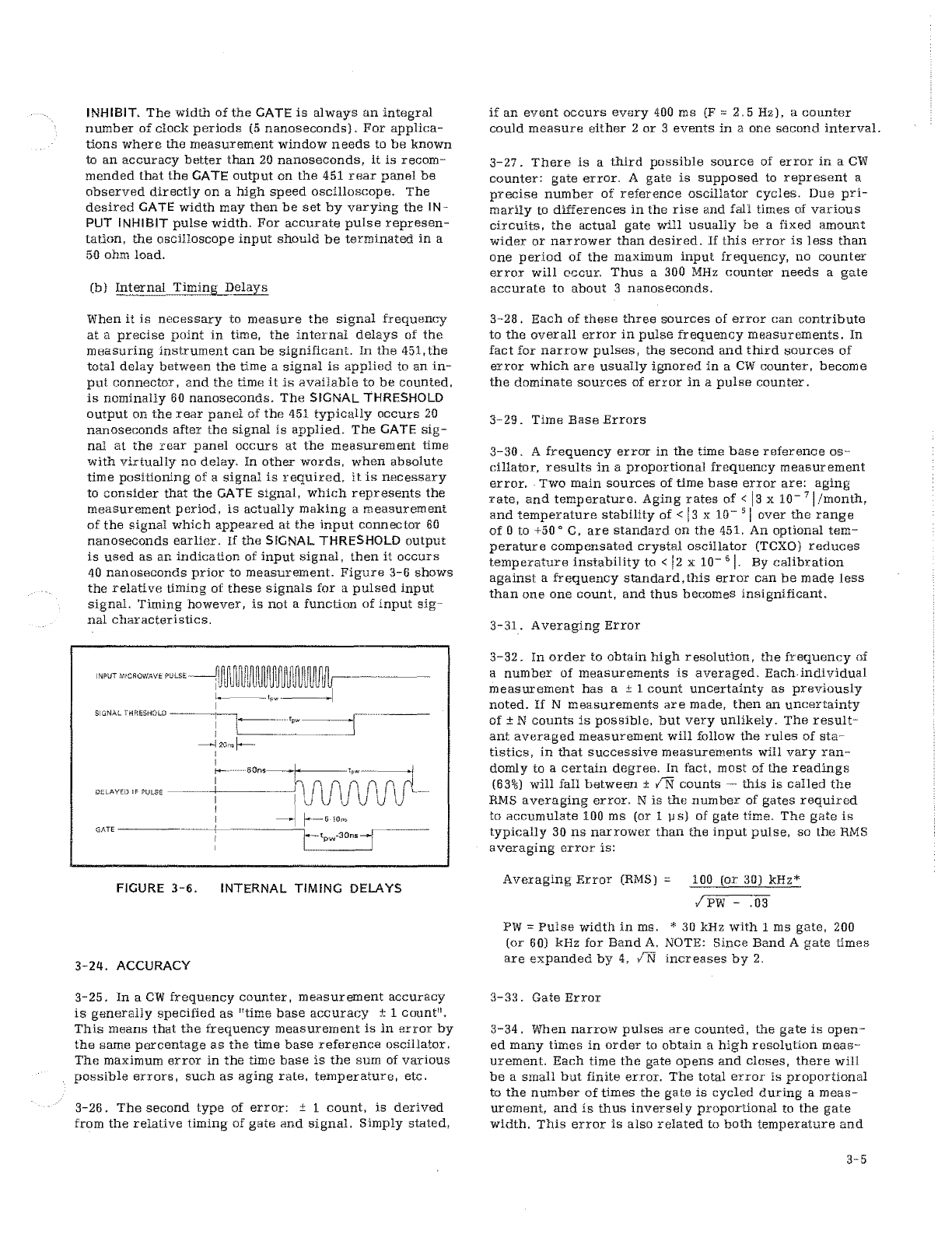
(b) Internal Timing Delays
When it is necessary to measure the signal frequency
at a precise point in time, the internal delays of the
measuring instrument can be significant. In the 451,the
total delay between the time a signal is applied to an in-
put connector. and the time it is available to be counted,
is nominally 60 nanoseconds. The SIGNAL THRESHOLD
output on the rear panel of the 451 typically occurs 20
nanoseconds after the signal is applied. The GATE sig-
nal at the rear panel occurs at the measurement time
with virtually no delay. In other words. when absolute
time positioning of a signal is required. it is necessary
to consider that the GATE signal, which represents the
measurement period, is actually making a measurement
of the signal which appeared at the input connector 60
nanoseconds earlier. If the SIGNAL THRESHOLD output
is used as an indication of input signal, then it occurs
40 nanoseconds prior to measurement. Figure 3-6 shows
the relative timing of these signals for a pulsed input
signal. Timing however, is not a function of input sig-
nal characteristics.
FIGURE 3-6. INTERNAL TIMING DELAYS
3-24. ACCURACY
3-25. In a CW frequency counter, measurement accuracy
is generally specified as time base accuracy ± 1 count".
This means that the frequency measurement is in error by
the same percentage as the time base reference oscillator.
The maximum error in the time base is the sum of various
possible errors, such as aging rate, temperature, etc.
3-26. The second type of errrate. 1 count, is derived
from the relative timing of gate acount.
nal. Simply stated,
if an event occurs every 400 ms (F = 2.5 Hz), a counter
could measure either 2 or 3 events in a one second interval.
3-27. There is a third possible source of error in a CW
counter: gate error. A gate is supposed to represent a
precise number of reference oscillator cycles. Due pri-
marily to differences in the rise and fall times of various
circuits, the actual gate will usually be a fixed am
circuits.
r or narrower than desired. If this error is less than
one period of the maximum input frequency, no counter
error will occur. Thus a 300 MHz counter needs a gate
accurate to about 3 nanoseconds,
3-28. Each of these three sources of error can contribute
to the overall error in pulse frequency measurements. In
fact for narrow pulses, the second and third sources of
error which pulses.
ally ignored in a CW counter, become
the dominate sources of error in a pulse counter.
3-29. Time Base Errors
3-30. A frequency error in the time base reference os-
cillator, results in a proportional frequency meaos-
cillator.
or. Two main sources of time base error are: aging
rate, and temperature. Aging rates of <13 x 10
- 7
1
rate.
h,
and temperature stability of <13 x 10
- 5
1 over the range
of 0 to +50° C, are standard on the 451. An optional tem-
perature compensated crystal oscillator (TCXO) reduces
temperature instability to <12 a 10
- 6
1.
By calibration
against a frequency standard,this error can be made less
than one one count, and thus becomes insignificant.
3-31. Averaging Error
3-32. In order to obtain high resolution, the frequency of
a number of measurements is averaged. Each-individual
measurement has a ± 1 count uncertainty as previously
noted. If N measurements are made, then an uncertainty
of ± N counts is possible, but very unlikely. The result-
ant averaged measurement will follow the rules of sta-
tistics, in that successive measurements will vary ran-
domly to a certain degree. In fact, most of the readings
(63%) will fall between ±
✓
IT]
.
counts — this is called the
RMS averaging error. N is the number of gates required
to accumulate 100 ms (or 1 es) of gate time. The gate is
typically 30 ns narrower than the input pulse, se the RMS
averaging error is:
Averaging Error (RMS) = 100 (or 30) kHz*
PW - .03
PW = Pulse width in ms. * 30 kHz with 1 ms gate, 200
(or 60) kHz for Band A. NOTE: Since Band A gate times
are expanded by 4,
7
--
N
increases by 2,
3-33. Gate Error
3-34. When narrow pulses are counted, the gate is open-
ed many times in order to obtain a high resolution meas-
urement. Each time the gate opens and closes, there will
be a small but finite error. The closes.
rror is proportional
to the number of times the gate is cycled during a meas-
urement, and is thus inversely proportional to the gate
width. This error is also related to both temperature and
3-5
AVERAGE READING
cw rsTo.
MEASUREMENT
LEAST
SIGNIFICANT
DI
However.this
TPUT
07
-
P
,
P
CHART
RECORDER
/
ANALOG
OUTPUT
DIGITAL
TO
ANALOG
CONVERTER
MICROWAVE
PULSE
COUNTER
input frequency. In the 451, the worst case error includ-
ing all variables. is specified as:
Max Gate Error =
40 kHz
PW - .03
where PW = pulse width in microseconds.
Unlike averaging error which is random, gate error is
systematic, and is not reduced by frequency averaging.
3-35. TECHNIQUES FOR IMPROVING ACCURACY
3-36. In most cases, specified accuracy of the 451 will be
more than sufficient to meet measurement requirements.
If greater accuracy is required, all three sources of error
can be minimized by a combination of error calibration
and long term averaging. It is recommended that if very
high accuracy is required, the counter include Options P1
(TCXO) and P4 (BCD Output/Remote Programming).
3-37. Time Base Calibration
3-38. A frequency error in the time base oscillator results
in the same percentage error in the frequency reading for
either. CW or pulsed signals. By directly measuring the 10
MHz time base frequency at the 10 MHz OUTPUT connector
using a standard of known accuracy, this error can be
determined and corrected. As an example, suppose the
measured time base output is 10.0001 MHz. The time base
is thus 1 x 10
- 6
high in frequency, and all readings will
be 1 x 10
- 6
low in frequency -- a reading at 10 GHz will
be 10 kHz low. Instead, of correcting the
reading
for this
error, a better technique is to set the time base oscillator
precisely on frequency. The advantage of a 451 equipped
with a TCXO is improved settability and temperature
stability.
3-39. Long Term Averaging
3-40. Averaging error, as noted previously, is simply
the result of a random statistical process. As in all such
processes, taking a larger number of samples reduces the
averaging error. On 451'8 equipped with BCD Output Op-
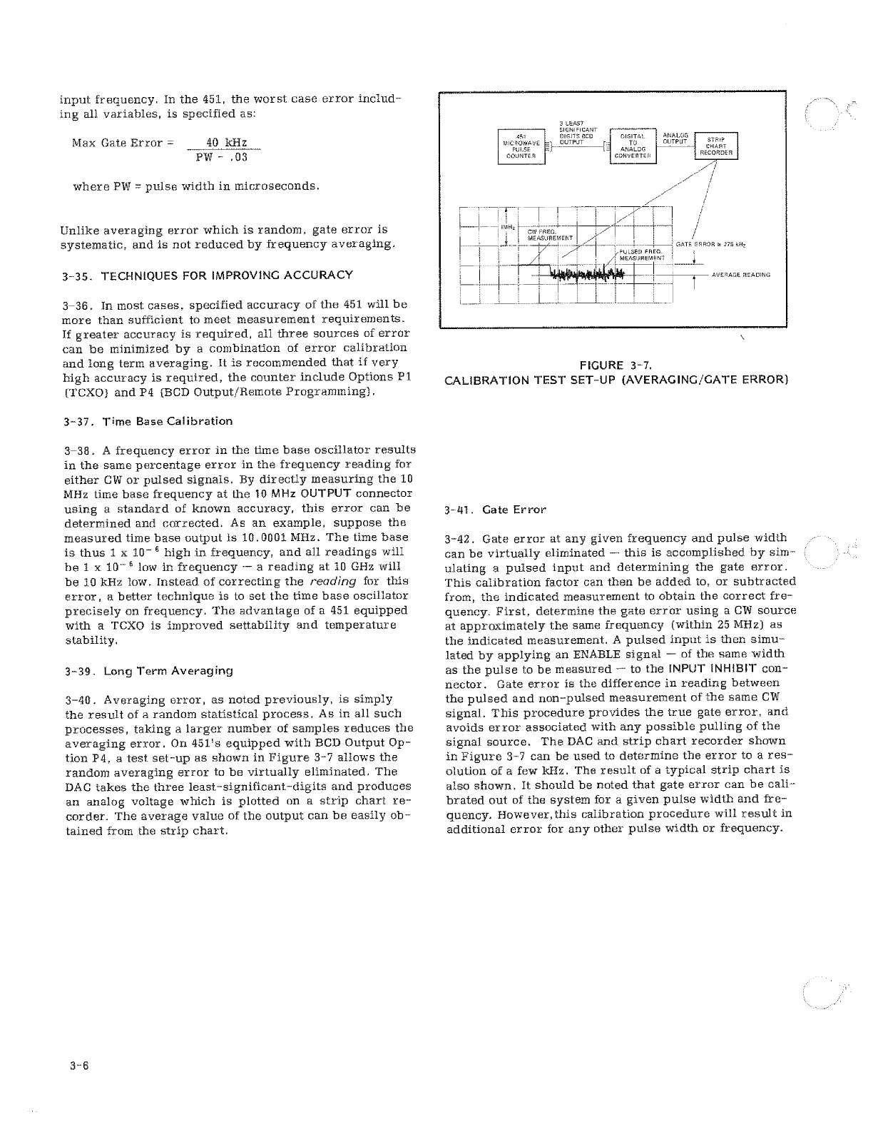
tion P4, a test set-up as shown in Figure 3-7 allows the
random averaging error to be virtually eliminated, The
DAC takes the three least-significant-digits and produces
an analog voltage which is plotted on a strip chart re-
corder. The average value of the output can be easily ob-
tained from the strip chart.
FIGURE 3-7.
CALIBRATION TEST SET-UP (AVERAGING/GATE ERROR)
3-41. Gate Error
3-42. Gate error at any given frequency and pulse width
can be virtually eliminated — this is accomplished by sim-
ulating a pulsed input and determining the gate error.
This calibration factor can then be added to, or subtracted
from, the indicated measurement to obtain the correct fre-
quency. First, determine the gate error using a CW source
at approximately the same frequency (within 25 MHz) as
the indicated measurement. A pulsed input is then simu-
lated by applying an ENABLE signal — of the same width
as the pulse to be measured — to
the INPUT INHIBIT
con-
nector. Gate error is the difference in reading between
the pulsed and non-pulsed measurement of the same CW
signal. This procedure provides the true gate error, and
avoids error associated with any possible pulling of the
signal source. The DAC and strip chart recorder shown
in Figure 3-7 can be used to determine the error to a res-
olution of a few kHz. The result of a typical strip chart is
also shown. It should be noted that gate error can be cali-
brated out of the system for a given pulse width and fre-
quency. However,this calibration procedure will result in
additional error for any other pulse width or frequency.

SECTION 4
GENERAL THEORY OF OPERATION
4-1. GENERAL
4-2. The EIP Model 451 Microwave Pulse Counter auto-
matically measures and displays the frequency of a CW
or pulsed signal in the range of 925 MHz to 18 GHz (Band
B). An optional Prescaler (Option P2} extends this range
downward to 300 MHz (Band A). In addition to fully auto-
matic measurements. it is possible to utilize the 451 with
accessory equipment to make dynamic frequency measure-
ments — the frequency of any repetitive signal can thus
be measured at any point in time. Measurement windows
as narrow as 20 nanoseconds are achievable.
4-3. Measurements in Band B (925 MHz - 18 GHz) are
achieved by heterodyning the input signal with a known
harmonic of 200 MHz. The resulting difference frequency
is then processed by a 350 MHz Direct Counter. The
counter gate is enabled by the input itself in a manner
such that the gate is open only when a signal is present.
4-4. In the Direct Counter, obtainable resolution is in-
versely proportional to the measurement time. For exam-
ple: a 1 microsecond gate time will yield 1 MHz resolu-
tion. To achieve 10 kHz resolution, the 451 automatically
averages as many input pulses as necessary to obtain a
total gate interval of 100 ms (or 1 us). The required
number of pulses is thus a function of the input pulse
width. (A more comprehensive discussion of this will be
found beginning with paragraph 4-27.)
4-5. In the optional Band A (300 MHz - 950 MHz), the in-
put frequency is divided by four. The divided frequency
is then counted in the Direct Counter for a 400 us (or
4 ms) period to obtain a readout with 10 kHz resolution.
As in Band B. gating is controlled by the input signal.
4-6. The system operation of the 451 is best described
by separating the instrument into its two main functional
blocks: the Microwave Converter. and the Direct Counter.
4-7. Figure 4-1 shows a simplified block diagram of the
entire 451. Figure 4-2 shows a more complete block dia-
gram of the Microwave Converter section, while Figure
4-3 diagrams the Direct Counter. Detailed circuit descrip-
tions of all PC boards are given in Section 9.
4
-
8. MICROWAVE CONVERTER
4-9, The Microwave Converter is a self-contained assem-
bly which performs the function of translating the input
microwave frequency downward into the range of 100 to
350 MHz. This translation is accomplished by mixing the
incoming signal with a known reference frequency and
then amplifying the difference. The input frequency is
determined by counting this difference frequency and ad-
ding it to the known reference frequency (see Figure 4-2).
4-10. The reference frequency is an integral harmonic of
200 MHz. generated within the FIG Comb Generator (A207).
This unit is an integrated assembly containing a harmonic
(or comb) generator,and a two-stage FIG filter. The comb
generator converts the 200 MHz sine wave input into a
train of narrow pulses containing all the harmonics of 200
MHz up to 18 GHz. while the FIG filter selects the desired
harmonic. Tuning of the FIG filter is accomplished by
varying the current through a pair of coils, which in turn,
varies a magnetic field within the structure. (A more com-
prehensive description of the operation of a FIG-tuned
device is given tater in this section.)
4-11. The 200 MHz reference is generated within Source/-
Amplifier A201 by an LC oscillator which is phase-locked
to the 10 MHz Time Base Oscillator (A108) within the 451.
This reference is amplified to produce up to one watt of
output power to drive the comb generator section of A207.
A second output at 200 MHz is used to generate the gate
and test functions within the Direct Counter.
4-12. The RF input signal to the Converter section first
passes through a Limiter/Attenuator (A206). The limiter
portion of this module is a passive diode whose main func-
tion is to protect the Mixer (A205) against excessive input
power. Protection at levels up to one watt peak or average
is provided.The attenuator section contains a multistage.
matched PIN diode serving two functions: (a) to provide a
means of controlling the RF signal level to the Mixer. and
(b) to act as a switch which shuts off the input signal dur-
ing certain portions of Converter operation.
4-13. The Mixer (A205) is another integrated microwave
circuit assembly, containing a hybrid coupler, termina-
tion, mixer diode, and a DC return. The Mixer produces
two output signals on a common line: (a) an IF signal
equal in frequency to the difference between the RF sig-
nal and the reference signal; (b) a Video signal resulting
from rectification of either the RF or reference input.
4-14. The IF and Video signals are separated in the IF
Processor (A204). This assembly contains an IF amplifier,
video amplifiers. threshold circuits, and LOCK circuitry.
The output of the IF amplifier is the signal actually meas-
ured by the Direct Counter. It is also used by the LOCK
circuitry to determine the correct reference frequency
(comb line). The Converter is considered to be locked
when a particular comb line mixes with the applied RF
signal to produce an IF signal of proper amplitude and
frequency.
4-15. The amplified Video output is used to generate three
separate signals: two threshold, and one analog output.
One signal — SIGNAL THRESHOLD — is used to detect the
presence of sufficient RF signal to initiate operation of the
Converter and enable the gate of the Direct Counter. The
4-1

FIGURE 4-1. BLOCK DIAGRAM - 4S1 MICROWAVE PULSE COUNTER
SALO
IKOLJT
_L
Iuvur
— FzEF
SIGL1AL
THRESHOL4>
0A1.42 S
THKESHOLD
> LOCK
can3vETe TE2 K.3ASLE
POP LIMIT
>
MSC
,
P2tSET
FIGURE 4-2. BLOCK DIAGRAM - 451 PULSE COUNTER - CONVERTER (A2)
4-2
Table of contents
Other EIP Cash Counter manuals

Popular Cash Counter manuals by other brands


Gemini
Gemini BPM-1 Service manual

MULTISPAN
MULTISPAN LC-2046 quick start guide

MEI
MEI Cashflow SC Series Operation & maintenance manual

Nautilus Hyosung
Nautilus Hyosung MONiMAX5600 Service manual

Measurement Computing
Measurement Computing CB-7080 user guide

advantest corporation
advantest corporation TR5821 Operation manual