Element14 PAN9028 M.2 User manual

User Guide
I N T R O D U C T I O N
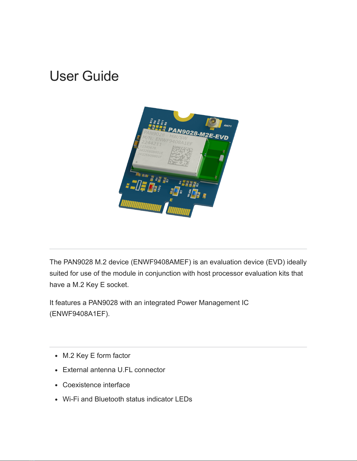
The PAN9028 M.2 device (ENWF9408AMEF) is an evaluation device (EVD) ideally
suited for use of the module in conjunction with host processor evaluation kits that
have a M.2 Key E socket.
It features a PAN9028 with an integrated Power Management IC
(ENWF9408A1EF).
F E AT U R E S
M.2 Key E form factor
External antenna U.FL connector
Coexistence interface
Wi-Fi and Bluetooth status indicator LEDs

PCM interface
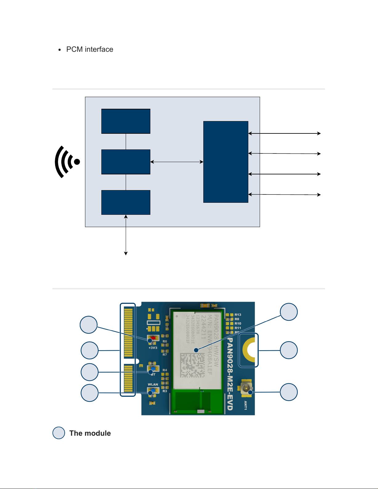
B L O C K D I A G R A M
Module M.2 Key E
Connector
PAN9028 M.2 Device
Highspeed-UART
for Bluetooth
U.FL
Connector
External
Antenna
Status LEDs
SDIO 3.0
for Wi-Fi
PCM
Interface
Coexistence
Interface
B O A R D O V E R V I E W
3
7
1
4
5
62
1 The module

2 Mounting screw indentation
You can use the Mounting screw indentation to secure the board in a M.2 Key
E socket. Also see
3 External antenna U.FL connector ANT1
You can use the U.FL connector to connect an external antenna. Also see
4 Wi-Fi status indicator LED
The Wi-Fi status indicator LED for indicating the Wi-Fi status is currently non-
operational.
5 Bluetooth status indicator LED
The Bluetooth status indicator LED for indicating the Bluetooth status is
currently non-operational.
6 M.2 Key E connector
You can insert the PAN9028 M.2 device into a M.2 Key E socket to connect
the modules interfaces to a host processor. Also see
7 Power LED
You can observe the Power LED to verify that the board is correctly powered.
D E V I C E D I M E N S I O N S
Mounting the Device
Antenna Configuration
M.2 Connector Pin Map

The PAN9028 M.2 device is secured in place.
M . 2 C O N N E C T O R P I N M A P
Description M.2 Key
E Pin
Function Module
Footprint
Module Pin
SDIO
Interface
9 SDIO CLK G5 SD_CLK
11 SDIO CMD G6 SD_CMD
13 SDIO DATA0 G7 SD_DAT0
15 SDIO DATA1 G8 SD_DAT1
17 SDIO DATA2 G9 SD_DAT2
19 SDIO DATA3 G10 SD_DAT3
UART
Interface
22 UART RXD /
GPIO8
B8 UART_SOUT /
IO8
32 UART TXD / GPIO9 A8 UART_SIN /
IO9
34 UART RTS /
GPIO11
A7 UART_RTS /
IO11
36 UART CTS /
GPIO10
B8 UART_CTS /
IO10
Status LEDs 6 Wi-Fi LED / GPIO2 F8 LED_WLAN /
IO2
16 Bluetooth LED /
GPIO3
F9 LED_BT / IO3

Description M.2 Key
E Pin
Function Module
Footprint
Module Pin
PCM
Interface
8 I2S SCK / GPIO6 E1 PCM_CLK / IO6
10 I2S WS / GPIO7 F6 PCM_SYNC /
IO7
12 I2S SD IN / GPIO5 F7 PCM_DOUT /
IO5
14 I2S SD OUT /
GPIO4
F10 PCM_DIN / IO4
Coexistence
Interface
46 Coexistence RXD /
GPIO17
B10 COEX_OUT /
IO17
48 Coexistence TXD /
GPIO16
F5 COEX_SIN /
IO16
Clock 50 32 KHz Oscillator E6 32KHZ_IN
Power 2, 4, 72,
74
3.3 V F2, F3 VDD3V3
56 PMIC Enable A2 PMIC_EN
1, 7, 18,
33,
39, 45,
57, 63,
69, 75
GND A1, A12, B12,
C11, C12,
D11,
D12, E11,
E12,
F1, F11, F12,
G11, EP1,
EP2,
EP3, EP4
GND,
EPAD1,
EPAD2,
EPAD3,
EPAD4

Description M.2 Key
E Pin
Function Module
Footprint
Module Pin
not
connected
3, 5, 7,
20,
21, 23,
35, 37,
38, 40,
41, 42,
43, 44,
47, 49,
52, 53,
54, 55,
58, 59,
60, 61,
62, 64,
65, 66,
67, 68,
70, 71,
73
not connected N/A N/A

The UART_SOUT (M.2 Key E pin 22) doubles as a configuration
pin for the clock frequency used by the PAN9028.
Only the 26 MHz configuration is valid since the PAN9028 includes
a crystal with this frequency.
Keep this pin floating or on logical high level during firmware
initialization. A low level during firmware initialization prevents the
firmware from starting up.
H A R D W A R E M O D I F I C AT I O N S
You can modify the PAN9028 M.2 device to suit your application and your specific
host processor by making some hardware modifications.
The following sections describe how you can reconfigure the reference voltages
and how you activate the 3.
SDIO Reference Voltage
In case your host processor board only supports a SDIO signal voltage of 3.3 V
you can reconfigure the PAN9028 M.2 device to use the 3.3 V generated by the
PMIC as VIOSD.
The PAN9028 supports 1-bit or 4-bit SDIO transfer modes with full clock range up
to 208 MHz. The SDIO Interface pins are powered from the VIOSD voltage supply
with either 1.8 V or 3.3 V.
On the PAN9028 M.2 device by default VIOSD is connected to the VOUT1V8 of the
PMIC, hence it is set to 1.8 V.
Clock Configuration Pin
external antenna U.FL connector ANT1

Setting VIOSD to 3.3 V also configures the IO reference voltage to
be 3.3 V as well.
To set VIOSD to 3.3 V execute the following instructions.
1. Unsolder the resistors R8 and R9.
2. Place a 0 Ohm resistor (0402) for R13 and or bridge it with a solder blob.
3. Place a 0 Ohm resistor (0402) for R10 and or bridge it with a solder blob.
IO Reference Voltage

This connects VIOSD to 3.3 V.
SDIO clock speeds higher than 50 MHz can only be achieved with
a SDIO signal voltage level (VIOSD) of 1.8 V and a host processor
that supports the SDIO 3.0 Standard.
The maximum achievable data rate is limited by the used SDIO
clock speed.
For further information please refer to the module product
specification .
IO Reference Voltage
In case your host processor board supports only IO voltage levels of 3.3 V you can
reconfigure the PAN9028 M.2 device to use 3.3 V as voltage level for its UART and
IOs.
The voltage used by the IOs and the UART interface is determined by the voltage
applied to VIO. You can configure it to either 1.8 V or 3.3 V.
Note
PAN9028 Product Specification

On the PAN9028 M.2 device by default VIO is connected to VOUT1V8 of the PMIC,
hence it is set to 1.8 V.
In case you have set VIOSD to 3.3 V as described in
the IO reference voltage is also
configured to be 3.3 V.
Please note, if VIOSD is set to 3.3 V it is not possible to set the IO
reference voltage to 1.8 V since this would create a short between
3.3 V and 1.8 V.
To set VIO to 3.3 V execute the following instructions.
1. Unsolder R8.
2. Place a 0 Ohm resistor (0402) for R13 or bridge it with a solder blob.
Warning
SDIO Reference Voltage

This connects VIO to 3.3 V.
Antenna Configuration
You can evaluate PAN9028 M.2 device in conjunction with an external antenna by
activating the 3 with some hardware
modifications. By default the chip antenna is active.
External Antenna
To activate the 3 execute the following
instructions.
1. Unsolder R3.
2. Place a 0 Ohm resistor (0402) for R4 or bridge it with a solder blob.
external antenna U.FL connector ANT1

This manual suits for next models
1
Table of contents
Other Element14 Motherboard manuals