SERIES 400 SECTION III
SECTION III
THEORY OF OPERATION
GENERAL
The Elgar Series 400 plug-in osci I lators all use simi-
lar low voltage power supplies and operational amplifier
filters, and draw operating power from the Elgar Power
Source. The amplitude of the output signal for all units
is controlled by the Power Source front panel AMPLI-
TUDE control (a potentiometer which is physically lo-
cated in the Power Source enclosure). The 0. 1% model
uses a positive feedback square wave input to the opera-
tional active filters. The closer tolerance models con-
tain a crystal oscillator, and a frequency dividing circuit
formed by a series of integrated circuit flip-flops. The
output of the oscillator is a symmetrical square wave free
from even harmonics.
GENERALCIRCUIT DESCRIPTION
The 0.01% and 0.0001% tolerance oscillators (see
Figure 3-1) generate the output frequency with a crystal
oscillator operating at a frequency near 100 KHz and a
chain of flip-flops which divide the oscillator frequency
by some power of two to generate the output frequency.
For example, 400 Hz is generated by a 102.4 KHz crys-
tal and then divided by 256 with 8 flip-flops. The
square wave output of the flip-flop chain is amplitude-
stabi lized by zener diode and then filtered in a two-
section active low-pass filter to remove the harmonic
distortion and produce a pure sine wave. The active
filter is tuned to peak response at the output frequency
and has 180° phase shift at the output frequency.
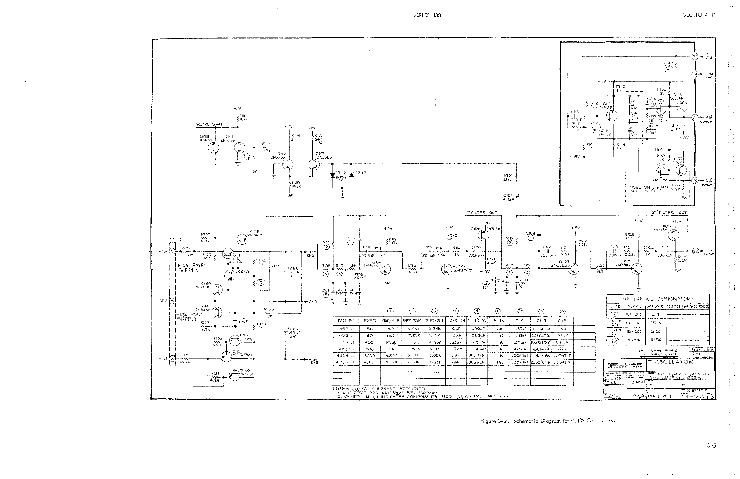
The 0.1% tolerance oscillators (see Figure 3-2 also
operate by generating a square wave and filtering it in a
two-section active filter. In these oscillators, however,
the square wave is generated by positive feedback around
the filter through an inverting clipper. The feedback
system oscillates at the frequency where the filter phase
shift is 180°.
A trimpot is provided to adjust the frequency of the
0.1% oscillators. The 0.01% oscillators do not require
afrequency adjustment. The 0.0001% oscillatorsrequire
an adjustment to compensate for crystal aging,
In the crystal-controlled oscillators, R101 and
diodes CR101 through CR I05 reduce an unregulated +42
VDC input from the power source to +3.6 VDC collector
voltage for the oscillator and integrated circuits. The
oscillator, which does not require an oven, consists of
the crystal and transistors Q 101 and Q102. The square
wave oscillator output is divided through an appropriate
number ofintegratedcircuit flip-flops to produce, at the
base of transistor Q103, a square wave at the output fre-
quency. The crystal frequency and number of dividing
flip-flops used for any output frequency is shown on the
table given in the schematic diagram. Transistor Q 103
is a saturated switch which switches the output from re-
sistor R107 to ground or across the anode of CR 106,
producing a symmetrical equal duty ratio square wave.
Half the time the output is +6,2 volts (approximately)
and the other half the time the output is ground. CR106
is a 2N3638 transistor used as a zener diode. The output
from the oscillator section is applied to the active filter
circuits through resistor R108, the value of which is de-
termined by oscillator frequency.
The filter circuits consist of two similar operational
amplifiers with frequency-selective feedback networks
which produce the filtering action. The first filter is
tuned by resistors R108, R109, and R110 and capac i tors
C102 and C 103. The values of these components depend
on the required output frequency, and can be determined
by consulting the table presented on the schematic dia-
gram. The first operational amplifier consists of transis-
tors Q 104, Q 105, and Q 106. The second fi !ter, in series
with the first, is tuned by resistors RI18, R119, and R120
and capacitors C107 and C 108. The second operational
amplifier consists of transistors Q107, Q108, and Q 109.
The plug-in oscillators operate on +42 VDC and -42
VDC supplied by the Power Source. The input voltage
is regulated at +15 VDC and -15 VDC in the plug-in
enclosure. Amplifier transistor Q110 compares the volt-
age developed across CR107 to the +15 VDC regulated
output, divided across resistors R132 and R133. The am-
plifier transistor Q114 compares the +15 VDC output to
the -15 VDC output. Regulation of both supplies is im-
proved by bootstrapping the amplifier collector load with
3-1
Artisan Technology Group - Quality Instrumentation ... Guaranteed | (888) 88-SOURCE | www.artisantg.com