elv SUP3 User manual
www.elv.com
2 Audio Technology
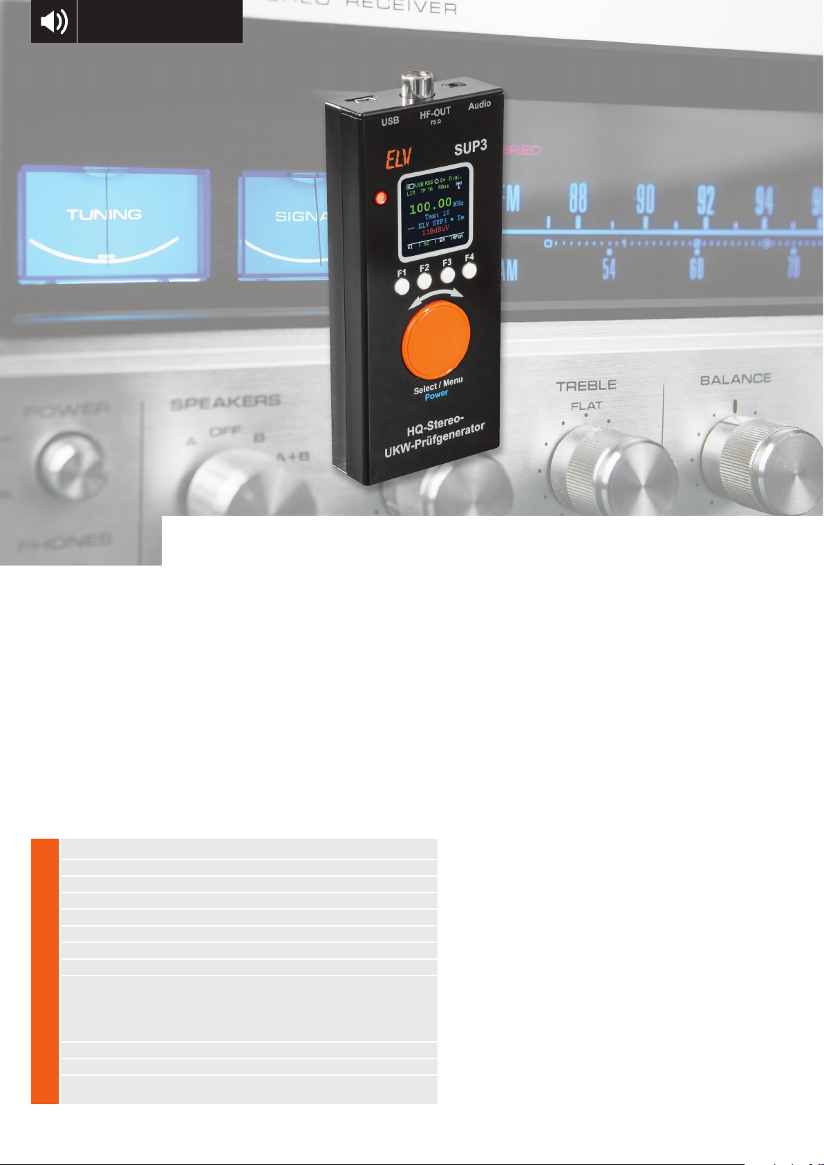
Versatile
After the great response to the predecessor models
SUP1 and SUP2, we present the successor, SUP3, which
has numerous new features. First of all, there is now
The SUP3 generates a high-quality FM signal including an individually configurable RDS signal. In additi-
on to the analogue audio feed, a USB interface also allows digital audio data to be fed in. The operation is
clearly arranged via a practical combination of rotary encoder and OLED display; in addition, PC software
allows easy control of the SUP3 from a PC.
Device short description: SUP3
Power supply: 2x 1,5 V LR6/Mignon/AA
Current consumption: 250 mA max.
Standby current: 10 μA
Frequency range: 87,5–108 MHz
HF-output: 88–118 dBμV/75 Ω/IEC
Audio-inputs: Audio-/Stereo-audio-jack
Display: OLED-colour-display with 128 x 128 pixel
Other: Audio optional analog (audio jack) or digital (USB)
Station name (2x 8 characters)
RDS-text (64 characters)
Operation and audio data (digital) via USB
Ambient temperature: 5 bis 35 °C
Dimensions (W x H x D): 63 x 142 x 25 mm
Weight (with/without batteries): 184/135 g
Technical data
a digital signal feed via USB. This allows you to use
a PC or other device with USB sound output directly
as a signal source. And since the VHF test generator
can also be operated with batteries and an RDS signal
to be output can be stored in its EEPROM, you can,
for example, use the mobile combination of test ge-
nerator and smartphone to put the coveted radio tre-
asure through its paces before buying it, even if, for
example, VHF reception is not possible in a particu-
lar space. Such a generator is also excellently suited
for demonstrating radios, whether in the showroom
or in a museum, as it makes the radio independent of
antenna reception and also offers the possibility of
outputting your own content, such as explanations in
an exhibition.
However, the main purpose of use is probably the
repair and restoration of VHF radio receivers. An ex-
act calibration is only possible with a test signal that
conforms to standards. The use as a VHF transmitter,
however, even if it is only for short distances, is pro-
hibited!
Perfect Signal Supplier
HQ Stereo VHF Test Generator SUP3
2 Audio Technology
www.elv.com
Audio Technology 3
The operation of the SUP3 has also changed. A
colour OLED display is now available. It is operated
comfortably with a rotary wheel (rotary encoder).
A very special feature, as already mentioned, is the
USB connection. This makes it possible to transfer
digital audio data from the PC to the SUP3. The SUP3
functions as an external sound card. Remote control
is also possible via the USB connection.
Change of Function
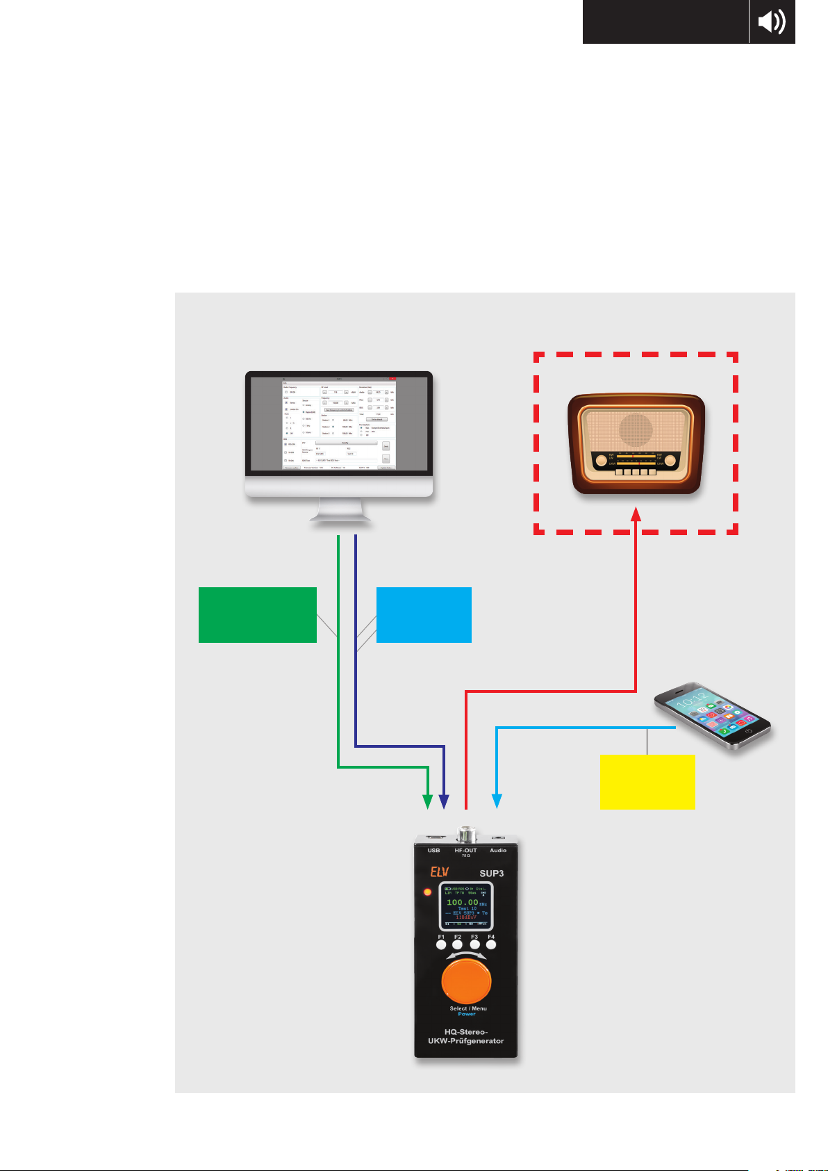
Fig. 1 shows the connection diagram for the SUP3
with all connection variants. The device under test
is shown here as a vintage radio. Please note that a
shielded cable must always be used as the connecting
cable to the device under test and must be connected
directly to the antenna input of the device. As already
mentioned, the SUP3 is a test generator and not a VHF
transmitter in the conventional sense. Therefore, HF
radiation must be avoided at all costs.
Figure 1: Connection diagram of SUP3
DUT Device Under Test
USB-Power
+
Control Commands
Digital
Audio data
PC
USB-HID
Analog
Audiodata
www.elv.com
4 Audio Technology
A smartphone, for example, can be used as an analogue audio source.
For the internal generation of test signals, the internal oscillator with
fixed frequencies of 100 Hz, 1 kHz or 10 kHz can also be used for modula-
tion (see Operation). Furthermore, it is possible to connect the SUP3 to
a PC via a USB connection. Two channels are used here. On the one hand,
the SUP3 can be conveniently controlled remotely via PC software and,
at the same time, a digital audio signal can be transmitted from the PC
to the SUP3. In this case, the SUP3 registers as an external sound card.
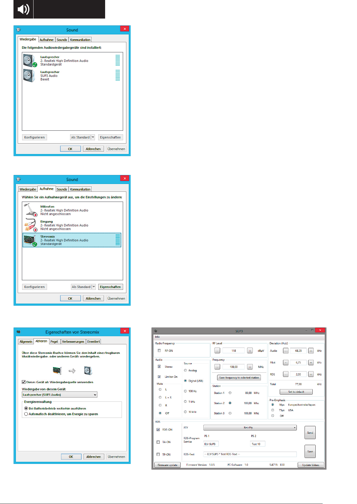
Setting up SUP3 on the PC
After the SUP3 has been connected via the USB port, it is automatically
recognised by the PC. For remote control, the SUP3 registers as an HID
device, so no driver is needed.
At the same time, an external sound card is recognised. The SUP3 can
now be selected as the output device under Speaker Properties. Please
note that Windows can only manage one sound card as an output source.
There is a little trick that allows you to listen to the audio signal on the
PC, namely „Stereo Mixer”:
To do this, go to Control Panel →Sound (Fig. 2) and under the Playback
tab the PC sound card and the SUP3 should be listed. Select the sound
card as the default device.
Under Recording you will find the Stereo Mixer (Fig. 3, if not: right click
and show deactivated devices and activate the stereo mixer). In the stereo
mixer settings in the Listening tab (Fig. 4), set the checkmark to Use this
device as playback source and select the SUP3 in the drop-down menu.
Then finish the setting with OK. Now the playback should take place on
both devices. Sometimes a restart of the computer is necessary.
During playback, latencies occur between the sound card and the out-
put on the device under test connected to the SUP3. This is due to the
different transmission paths.
PC-Software
The operating options, as shown in Fig. 5, are self-explanatory and cor-
respond to the operation on the unit, with the exception of the RDS
function. Here it is possible to change the RDS text and the text for the
RDS programme service directly. Pressing the Send key transmits the RDS
data to the SUP3. If you want to save the texts directly in the SUP3, this
is done by pressing the Save to EEprom SUP3 button.
Another special feature is the update function. A firmware update is
provided on the product page in the ELVshop (https://de.elv.com) if re-
Figure 2: Menu Sound under system settings
Figure 3: Under Recording you will find the stereo mixer
Figure 4: Set the checkmark to Use this device as playback
source Figure 5: You can adjust all settings via the PC software
www.elv.com
Audio Technology 5
quired. This may be the case if, for example, a firmwa-
re bug or the like is corrected. The FW file must first
be downloaded. Then select the downloaded file and
start the FW update. This process should not be inter-
rupted, otherwise a malfunction may occur.
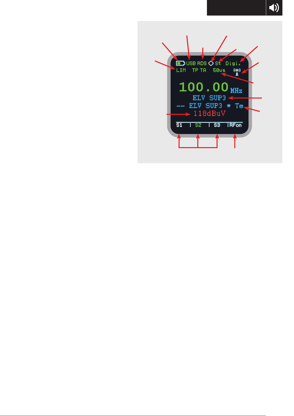
Operation
The unit is operated via a rotary wheel (rotary encoder)
and four function keys that perform different func-
tions depending on the menu. The unit is switched
on by pressing the rotary encoder. The Firmware ver-
sion first appears in the display. Then the main screen
appears. All the symbols are shown and explained in
Fig. 6. In the main screen, you can use the function
keys (F1 to F4) and the rotary encoder to carry out the
functions described below.
The function keys F1 to F3 can be used to call up
previously previously programmed frequencies (S1 to
S3). The fourth function key F4 is used to switch the
RF output (RFon) on and off. The active RF output is
indicated by an antenna symbol. The frequency can
be changed manually by turning the rotary encoder.
Pressing the push-button (rotary encoder) allows
you to enter the menu, which offers the following set-
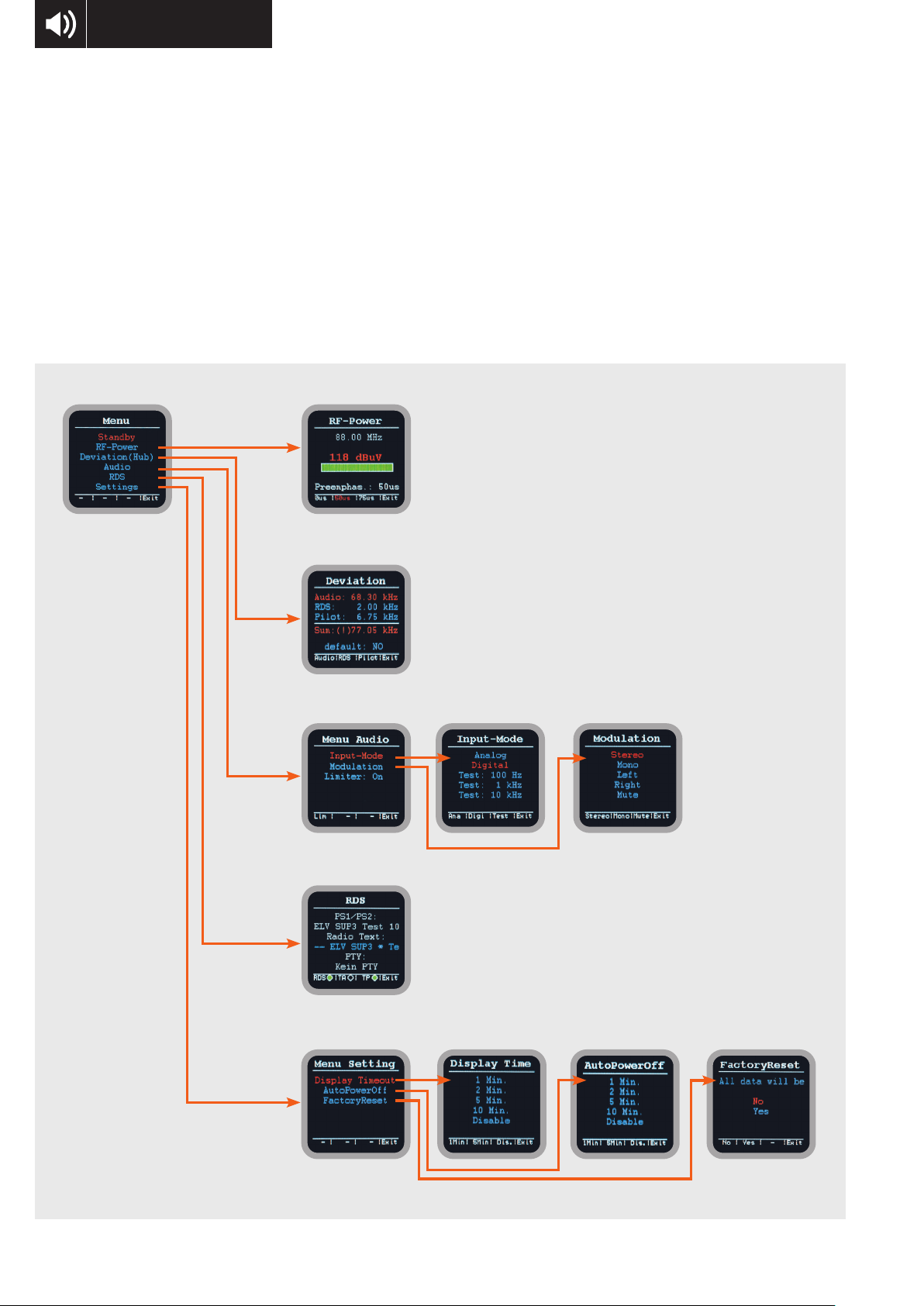
ting options and can be seen in the overview in Fig. 7:
RF Level (RF Power) and Pre-emphasis
Here, the output level can be changed in a range from
88 to 118 dBµV.
The function keys can be used to set the pre-em-
phasis. In Europe, a pre-emphasis of 50 µs is used [1].
The pre-emphasis is a transmitter-side treble boost
that is compensated by de-emphasis in the receiver.
This procedure is used to improve the signal-to-noise
ratio.
Deviation
The deviation depends on the modulation depth. In
FM modulation, the deviation indicates the volume of
the modulation signal. The greater the deviation, the
higher the volume [2]. The change in carrier frequen-
cy ∆fr is called frequency deviation. The deviation
can be set separately for themain carrier, RDS carrier
and pilot tone. According to the standard, the total
deviation must notexceed 77 kHz, because the carri-
ers can interfere with each other. For this reason, the
total deviation is displayed as a sum.
The function keys can be used to directly select
between the setting options, or the rotary encoder
can be used to advance. The respective value is chan-
ged with the rotary wheel. The menu can be exited
with the function key F4.
With Default, the basic settings for the deviation can
be restored. To do this, select this menu item by pres-
sing the rotary encoder and turn it to YES, then press
the encoder again to restore the default settings.
Under NO, the menu is closed without restoring the
basic settings.
„Audio“ Menu
In this menu you can select three submenus and acti-
vate or deactivate the limiter. The limiter can also be
switched with the function key F4.
Input Mode
Here you can select the source for the FM modulation. You can choose
between analogue input (jack socket), digital input (USB) or fixed fre-
quencies. By turning the rotary knob or using the function keys, you can
directly select between the inputs. To leave this menu, press the func-
tion key F4.
Note: No external analogue signal may be present during internal modula-
tion, as both signals mayoverlap.
Modulation
The functions can be activated using the rotary wheel. In addition, the
stereo, mono and mute functions can be activated directly via the func-
tion keys F1 to F3. Press the F4 key to leave this menu.
RDS
Press the F1 key to activate or deactivate the RDS function. Key F2 ac-
tivates the TA (Traffic Announcement) function. This causes a volume
increase on the receiver side if TP is also active.
When the function is activated, the corresponding circle next to the
function is filled in green.
The TP (Traffic Programme) function is activated with the F3 key.
TP identifies a station that offers traffic radio. Further information is
available at [3].
Menu Settings
With Display Timeout you can set the time after which the display swit-
ches off (1‒10 min). The set functions remain active. Disable activates
the display permanently, but this is not recommended, as switching it
on permanently can lead to premature failure at the end of the limited
service life of OLED displays.
Auto Power Off
This setting only applies to battery operation.
With Auto Power Off you can set a time after which the unit switches
off after the last operation (1‒10 min). With Disable or when supplied via
USB, the unit does not switch off automatically.
Battery
status
USB
connected
Limiter enabled
when red lights up Input
(analog/
digital)
Symbol for
enabled
RF-Output
Preemphasis
0/50 µs/75 µs
RDS-Text
RDS
station
name
RDS (TP, TA)
enabled Stereo/Mono
RF-output
(on/of f)
Set frequencies 1‒3
(programmable)
Limiter
enabled
RF Output-
Level
Figure 6: All possible elements of the display
www.elv.com
6 Audio Technology
Factory Reset
Due to the large number of setting options, various
setting parameters can be changed. To return to the
delivery status, there is the so-called factory reset. If
you select this option, all parameters are reset to the
factory settings.
Circuitry
The circuit diagram of the SUP3 (Fig. 8 and 8a) is di-
vided into the following circuit sections: analogue
input circuit, FM transmitter, controller with OLED
display and power supply.
Let‘s look at the input circuit first, which is shown in the upper part of
the circuit diagram. The analogue audio signal (stereo) is fed to the cir-
cuit via the socket BU11, which first reaches a limiter. The diodes D25 to
D27 are Transient Voltage Suppressor diodes which protect against over-
voltage or voltage peaks. The limiter IC14 of the type NJM2761 ensures
that a certain audio level cannot be exceeded; the limiter function can
also be deactivated via the menu. The output level is determined by the
resistor R3, which is 0.6 Vpp in this configuration. This means that the
maximum permissible level for the FM transmitter is not exceeded. C7
sets the time constant for the control.
From the limiter output, the two stereo signals are fed to a 2nd order
low-pass filter with a cut-off frequency of 15 kHz, which consists of the
Figure 7: Menu diagram of SUP3

www.elv.com
Audio Technology 7
Figure 8: Circuit diagram SUP3
5
4
3
2
1
TPS61040DBV
IC4
GND
FB
SW
EN
Vin
16V
10u
C67
50V
100n
C71
50V
22p
C68
820K
R61
270K
R62
BAT54J
D4
3,3uH/1,1A
L1
IRLML
6401
T6
10K
R58
PTC 16V
0,35A
R57
1,5V
Mignon
BAT2
1,5V
Mignon
BAT1
+UBat
PWREN
MP14
2M2
R64
220K
R65
TPS61040DBV
1
2
3
4
5
IC6
GND
FB
SW
EN
Vin
C77
10u
16V
C79
10u
50V
C80
10u
50V
C81
100n
50V
BAT54J
D5
6,8uH/0,94A
L2
+U-OLED
50V
22p
C78
12
11
10
9
8
7
6
5
4
3
2
1
BU4
12
11
10
9
8
7
6
5
4
3
2
1
BU5
12
11
10
9
8
7
6
5
4
3
2
1
BU6
10
9
8
7
6
5
4
3
2
1
ST1*
62
61
60
59
58
57
56
55
54
53
52
51
50
49
46
45
44
43
42
41
40
39
38
37
36
35
34
33
30
29
28
27
26
25
24
23
22
21
20
17
16
15
14
11
10
9
8
7
6
5
4
3
2
1
STM32F107RC
IC3
PC12
PC11
PC10
PC9
PC8
PC7
PC6
PC5
PC4
PC3
PC2
PC1
PC0
PD2
NRST
BOOT0
VBAT
PD0 OSC_IN
PD1 OSC_OUT
PB15
PB14
PB13
PB12
PB11
PB10
PB9
PB1
PB0
PB2 BOOT1
PB3 JTDO
PB4 JNTRST
PB5
PB6
PB7
PB8
PA0 WKUP
PC15 OSC32_OUT
PC14 OSC32_IN
PC13 TAMPER RTC
PA15 JTDI
PA14 JTCK SWCLK
PA13 JTMS SWDIO
PA12
PA11
PA10
PA9
PA8
PA7
PA6
PA5
PA4
PA3
PA2
PA1
64
63
48
47
32
31
19
18
13
12
STM32F
107RC
IC3
GNDGND GNDGND AGND
VccVcc VccVcc AVcc
24 MHz
Q1
16V
100n
C59
50V
10n
C60
50V
1n
C61
16V
1u
C62
10V
Tantal
47u
C66+
100n
16V
C56
10n
50V
C57
1n
50V
C58
100n
16V
C53
10n
50V
C54
1n
50V
C55
100n
16V
C50
10n
50V
C51
1n
50V
C52
+VSTM
100n
16V
C63
10n
50V
C64
1n
50V
C65
47u
10V
Tantal
C48+
50V
27p
C42
50V
27p
C43
0R
R41+U-OLED
5
4
2
3
1
Inkrementalgeber
mit Taster
DR1
C
B
A
16V
100n
C30
16V
100n
C31
16V
100n
C32
TA1
100n
16V
C44
TA2
16V
100n
C45
TA3
16V
100n
C46
TA4
16V
100n
C47
IRLML
6401
T4
T5
BC847C
10K
R47
100K
R46
220K
R25
220K
R26
1K
R43
10K
R54
220K
R42
16V
100n
C23
+UBat
50V
100p
C36
50V
100p
C37
50V
100p
C38
50V
100p
C39
50V
100p
C40
50V
100p
C41
100K
R37
100K
R36
100K
R39
100K
R35
10K
R38
6
5
4
3
2
1
PRG1
+UB
RST
TX
RX
BOOT
GND
100n
16V
C35
10K
R34
S-1206B33
U3T1
IC5
GND
IN OUT
IRLML
6401
T7
IRLML
6401
T8
16V
100n
C75
16V
100n
C74
16V
10u
C76
10K
R55
MP16
MP15
MP17
MP18
MP19
MP20 MP21 MP22
MP4
MP5
MP6
+VSTM
BAT54J
D7 C72
10V
Tantal
220u
+
220u
10V
Tantal
C73+
BC847C
T11
10K
R59
100K
R60
10K
R63
OLED_Pwr
16V
4u7
C49
22R
R56
+5VUSB
1K
R32
10K
R33
C10
1u
16V
C9
1u /16V
R7
47K
R8
47K
R9
100K
R10
1K8
R11
12K
C13
50V
680p
R14
470R
C11
50V
10n
C17
16V
1u
C16
1u /16V
R17
47K
R18
47K
R19
100K
R20
1K8
R21
12K
C20
680p
50V
R24
470R
C18
10n
50V
C1
1u/50V
C2
1u
50V
C4
100n
16V
R2
470R
R1
470R
D25
ESD9B5.0ST5G
D26
ESD9B5.0ST5G
D27
ESD9B5.0ST5G
C3
50V
1u
C6
16V
100n
C5
16V
2u2
BU11
6
5
4
3
2
1
Stereo
Klinkenbuchse
R3
10K
C7
16V
220n
C8
1u /16V
DAC1
C15
1u /16V
DAC2
IC13
4
8
TLV272ID
7
5
6
IC13
TLV272ID
B
-
+
+
C12
16V
1u
C19
16V
1u
IC14
10
98
7
6
5
4
32
1
NJM2761
INT
SENSE
SW
OUT_B
OUT_A
VREF
GND
V+
IN_B
IN_A
+5VUSB
+UB+3.3V
10u
50V
C69
10u
50V
C70
+VSTM
SP0503BAHTG
1
234
D24
+5VUSB
10n
50V
C34
Ferrit
L3
22RR31
22RR29
1K5R28
USB-Buchse
1
2
3
4
5
6
BU9PTC6V/0,5A
R27
100n
100V
C33
16V
22n
C26
+3.3V
10K R50
100n
16V
C29
Antennen-
buchse
BU10
10K
R53
BC848C
T14
16V
100n
C25
+3.3V
+3.3V
10K
R52
19
18
17
16
15
14
13
12
11
10
9
8
7
6
5
4
3
Si4711
IC12
VDD
GND
DFS
DIN
LIN
RIN
/SEN
SCLK
SDIO
/RST
VIO
GPO1
GPIO2/IRQ
GPIO3/DCLK
RCLK
TXO
RFGND
10K
R51
10p
50V
C27
+UB
RCLK
D6
1N4148W
1N4148W
D28
MP23
10K
R40
T15
IRLML
2502PbF
1M
R45
16V
1u
C24
+5VUSB
PWREN
DAC1
DAC2
RCLK
C22
16V
100n
4K7 R49
4K7 R48
L7
Ferrit
L8
Ferrit
L5
Ferrit
120nH
L4 10p
50V
C28
1K5
R6
1K5
R16
C82
100n
16V
D29
1N4148W
+3.3V
10K
R44
220R
R30
+VSTM
+VSTM
+VSTM
OLED_Pwr
R67
10K R66
10K
1K5
R5
1K5
R15
IC15
HT-7544-1
GND
IN OUT
C84
22u
10V
Tantal
+
C83
1u
16V
BAT_EN
+4.4V
+UB
BAT_EN
+VSTM
+4.4V
+4.4V
+4.4V
10K
R4
Lim_EN
Lim_EN
+4.4V
orange
D30
1
3
2
IC13
TLV272ID
-
+
+
A
F3
ST4*
1
2
3
4
Data lines
Control lines
Supply
4F1F F2 F3
n.i.p.
USB 2.0
Interface
RF-
OU
T
Audio
IN
Analog
Limiter
Low-Pass
FM-Transmitter
Microcontroller
Power supply
OLED

www.elv.com
8 Audio Technology
+13V VDDIO
+13V
ST1
12
11
10
9
8
7
6
5
4
3
2
1
ST2
12
11
10
9
8
7
6
5
4
3
2
1
ST3
12
11
10
9
8
7
6
5
4
3
2
1
LCD1
OLED-Display
1
2
3
4
5
6
7
8
9
10
11
12
13
14
15
16
17
18
19
20
21
22
23
24
25
26
27
28
29
30
NC
NC
NC
NC
VCC
VCOMH
VDDIO
VSL
D0
D1
D2
D3
D4
D5
D6
D7
R/W
E/RD
RES
D/C
CS
BS0
BS1
IREF
VDD
GPIO0
VCI
VSS
GPIO1
NC
1u
50V
C4
1u
50V
C5
1u
50V
C6
1u
50V
C2
1u
50V
C3
100n
50V
C1
50V
100n
C7
560K
R1
49R9
R2
1N4148W
D1
1N4148W
D2
Power supply
with ground
Data lines
Control lines
and IC-supply
Figure 8A. Circuit
diagram OLED-
display
two amplifiers IC13A and IC13B. Audio frequencies
above this cut-off frequency would be outside the
specification for the FM signal and would negatively
influence the frequency spectrum. The audio signal
processed in this way now reaches the inputs (LIN and
RIN) of the FM transmitter IC12 of type Si4711. This
component contains all the components that are ne-
cessary to generate a standard FM signal. IC12 is a DSP
(Digital Signal Processor) from Silicon Labs. The digi-
tal processing results in excellent technical data that
cannot be realised with reasonable analogue circuit
technology. The modulated RF signal is decoupled at
the output TXO (pin 4) and reaches the output socket
BU10 via the capacitor C28. The Si4711 can process
both analogue and digital audio signals. We have just
described the analogue signal path. The digital audio
data is fed via the pins DFS (pin 14) and DIN (pin 13).
Furthermore, the Si4711 can be controlled via an IC
interface. The Si4711 is configured via the lines SCLK
(pin 7) and SDIO (pin 8) with the help of the micro-
controller IC3. Special registers are used to set the
transmission frequency and the output level, for ex-
ample.
The afore-mentioned micro-controller IC3 of the
type STM 32F107RC, is the main control element of
the switch control. With the help of the OLED display, the rotary enco-
der DR1 and the four function keys (TA1 to TA4), a convenient operating
unit is created. The Si4711 is programmed via the IC bus according to the
desired function. A special feature is the USB interface, which fulfils two
functions: control, i.e. remote operation from a PC, and the transmis-
sion of digital audio data. When connected to a PC, an HID device and
an external sound card are recognised. The SUP3 then works as a sound
card, while at the same time being operated via USB. The audio data is
converted by the micro-controller IC3 into a format required for the FM
transmitter.
The USB interface is located at socket BU9. At the same time power
can also be supplied via the USB interface. The 5 V supply voltage from
the USB socket is fed to the circuit via the fusible resistor R27. The diode
array D24 protects the data lines of the USB connection from overvoltage
peaks.
Let‘s now take a look at the power supply, which is shown in the lower
part of the diagram. The circuit can be powered either by two non-rechar-
geable batteries or by the USB port. To make effective use of the batte-
ry voltage, a step-up converter is used to generate a constant voltage
of 5 V. This step-up converter is formed by IC4. The peripherals include
the storage coil L1 and the diode D4. The output voltage is set with the
voltage divider R61/R62. We do not want to explain the functioning of a
switching regulator in detail here. The battery voltage is switched with
transistor T6. In order to be able to switch the circuit on and off with the
integrated push-button of the rotary encoder, there is a network of swit-

www.elv.com
Audio Technology 9
ching transistors, the function of which is not easy to recognise at first
glance. When switched off, i. e. when transistor T6 is blocked, the battery
voltage (+UBat) is applied to the button of rotary encoder DR1 via resis-
Figure 9: Board photos and placement information of SUP3 (Top/ Bottom)
sembled in the usual way using the parts list and the
assembly plan, but the board photos shown (Fig. 9)
also provide helpful additional information.
tor R58 and diode D29. When the but-
ton is pressed, T6 becomes conducti-
ve and the controller is supplied with
voltage. The controller then outputs
a voltage at the „PWREN“ port, which
puts transistor T11 into the conduc-
tive state. This activates a latch that
switches transistor T6 through. Now
let‘s look at the further voltage path
from the output of the step-up con-
verter. The two transistors T7 and T8
serve as switches to interrupt the vol-
tage supply of the step-up converter
when it is supplied via the USB con-
nection. This happens automatically
as soon as the voltage (+5VUSB) is
applied to the gate of the two transis-
tors. The 5V voltage thus comes eit-
her from the USB socket or from the
step-up converter. The USB voltage
always has the highest priority. The
following voltage regulator IC5 gene-
rates a stable voltage of 3.3 V to sup-
ply the controller. The second voltage
regulator IC15 provides a voltage of
4.4 V for the analogue input circuit.
For the OLED display a voltage of 13 V
is required. The voltage is generated
with another step-up converter (IC6).
The structure is similar to that of IC4
with the difference that the output
voltage is higher here (13 V).
A colour OLED display is provided
for visualisation. Via the BU4 to BU6,
data and the required voltages of 3.3
and 13 V (UOLED) are supplied. Figure
8a shows the circuit of the OLED dis-
play module. In addition to the 3.3 V
for the display controller, which are
supplied via pins 1 and 2 of the so-
cket connector BU5, the OLED display
requires an additional 13 V voltage
for the panel. This „panel voltage“ is
made available to the display via pins
1 to 6 of the socket connector BU6. On
the display board there are only the
components needed to operate the
OLED and the three pins that connect
to the base board.
Build
The circuit of the SUP3 is placed on a
multilayer board with 4 layers. One in-
ner layer contains a complete ground
plane, which is the only way to avoid
undesired interference.
The board is pre-assembled with
SMD components so that only a few
wired components have to be assem-
bled. The wired components are as-

www.elv.com
10 Audio Technology
We start the assembly work by inserting the socket
BU10, which is inserted into the board from above and
soldered to the underside of the board. The rotary en-
coder DR1 is then inserted and soldered in the same
way.
Make sure that the socket lies flat on the board
and is exactly aligned. Only then will the sockets fit
through the recesses in the housing. All connecting
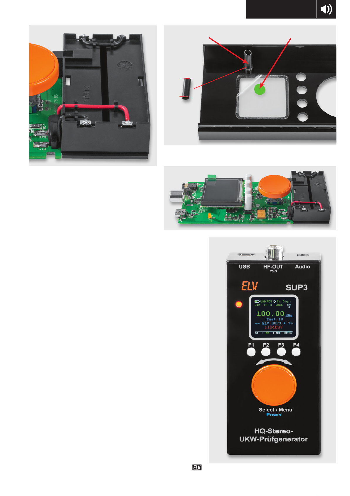
Figure 10: The LED is soldered directly and with no distance to the pcb
Figure 11: The individual steps to build the OLED-display
1 Gluing the display frame
2 Opening the connector
3 Inserting the OLED-display into the connector
4 Gluing the OLED-display into the frame
Figure 12: The battery holder ist to be equipped with the battery contacts and the connecting wires
– +
wires of this and the following components must be shortened to a maxi-
mum length of about 3 mm, if necessary.
Next, the light emitting diode D30 is installed. Make sure that the
polarity is correct. The slightly longer connection is the anode (+) of the
LED. The anode connection is also marked „+“ on the PCB. The LED can
rest directly on the PCB without any gap (see Fig. 10). This completes the
assembly of the main board.
Now we come to the preparation of the display board. The individual
steps are summarised in Fig. 11. Here, too, all SMD components are pre-
assembled. The frame has some catches that fit into the corresponding
openings of the display board to prevent it from being mounted incor-
rectly. This should be tested in advance, as it is very difficult to remo-
ve a sticky display frame afterwards. So that the display frame can be
mounted on the display board, the protective film on the underside must
first be removed and the frame must then be pressed onto the top of the
module with the aid of the latching lugs.
The next step is to attach the actual OLED display to the frame. First,
the contact connection on the underside of the module is opened by mo-
ving the small lever, which is then perpendicular to the board. Now the
www.elv.com
Audio Technology 11
Figure 13: Detail of assembly and connections for mounting the
battery compartment on the pcb
Figure 14: The insulating tube has to be pushed over the light guide to avoid any light
scattering
Figure 15:
Fully assembled pcb
of SUP3
Push insulating tube on light guide Remove adhesive foil
15 mm
Figure 16: SUP3 Fully assembled and ready for operation
contact foil of the display can be inserted into the connection and the
lever pressed down again. In this step it is important to ensure that the
display is not inserted the wrong way round. You can check the correct
installation with the help of Fig. 11. Finally, the protective film of the
second adhesive strip is removed and the glass body of the OLED is glued
into the frame with light pressure.
After the display board has been assembled, it can be plugged onto
the base board. Special care should be taken here, as the pin strips are
very sensitive and can bend easily. Make sure that the pin strips are not
plugged in at an offset, as this could lead to a malfunction or destruction
of components during testing.
Next, the battery holder must be pre-assembled. To do this, insert the
four battery contacts into the battery holder with the correct polarity
(Fig. 12). Make sure that the contacts engage properly. As can be seen in
Fig. 12 on the right, the contacts on the left-hand side must be bridged
with the enclosed stranded wire. The two remaining free contacts are
provided with the enclosed stranded wire, which is laid through the
cable guides, as also shown in Fig. 12 on the right. Finally, screw the bat-
tery holder to the circuit board with the enclosed screws and solder the
stranded wire to the solder pads S12 (+) and ST3 (-) provided (see Fig.13).
The light guide and display screen are already pre-assembled in the
upper part of the housing. Here, only a piece of insulating tubing needs
to be placed on the light guide (see Fig. 14). This prevents the light from
the LED from shining into the display window from the side. The insula-
ting tube must be shortened to a length of 15 mm. The display window is
covered on both sides with a protective film that still has to be removed.
Before installing the housing, caps for the buttons and the rotary en-
coder must be fitted. The hand-wheel for the Rotary encoder consists
of two individual parts that are simply plugged together. Fig. 15 shows
the completed circuit board. Now the batteries can be inserted and the
board can be placed in the bottom shell of the housing.
Finally, both halves of the housing are pushed together. Fig. 16 shows
the unit ready for operation.

www.elv.com
12 Audio Technology
Resistors:
0 Ω/SMD/0402 R41
22 Ω/SMD/0402 R29, R31, R56
220 Ω/SMD/0402 R30
470 Ω/SMD/0402 R1, R2, R14, R24
1 kΩ/SMD/0402 R32, R43
1,5 kΩ/SMD/0402 R5, R6, R15, R16, R28
1,8 kΩ/SMD/0402 R10, R20
4,7 kΩ/SMD/0402 R48, R49
10 kΩ/SMD/0402 R3, R4, R33, R34, R38, R40, R44, R47,
R50–R55, R58, R59, R63, R66, R67
12 kΩ/SMD/0402 R11, R21
47 kΩ/SMD/0402 R7, R8, R17, R18,
100 kΩ/SMD/0402 R9, R19, R35–R37, R39, R46, R60
220 kΩ/SMD/0402 R25, R26, R42, R65
270 kΩ/SMD/0402 R62
820 kΩ/SMD/0402 R61
1 MΩ/SMD/0402 R45
2,2 MΩ/SMD/0402 R64
PTC/0,5 A/6 V/SMD/0805 R27
PTC/0,35 A/16 V/SMD/1206 R57
Capacitors:
10pF/SMD/0402 C28
10 pF/50 V/SMD/0402 C27
22 pF/50 V/SMD/0402 C68, C78
27 pF/50 V/SMD/0402 C42, C43
100 pF/50 V/SMD/0402 C36–C41
680 pF/50 V/SMD/0402 C13, C20
1 nF/50 V/SMD/0402 C52, C55, C58, C61, C65
10 nF/50 V/SMD/0402 C11, C18, C34, C51, C54, C57, C60, C64
22 nF/16 V/SMD/0402 C26
100 nF/16 V/SMD/0402 C4, C6, C22, C23, C25,
C29–C32, C35, C44–C47,
C50, C53, C56, C59, C63, C74, C75, C82
100 nF/50 V/SMD/0603 C71, C81
100 nF/100 V/SMD/0805 C33
220 nF/16 V/SMD/0402 C7
1 µF/16 V/SMD/0402 C10, C12, C15–C17,
C8, C9, C19, C24, C62, C83
1 µF/50 V/SMD/0603 C1–C3
2,2 µF/16 V/SMD/0805 C5
4,7 µF/16 V/SMD/0805 C49
10 µF/16 V/SMD/0805 C67, C76, C77
10 µF/50 V/SMD/1210 C69, C70, C79, C80
22 µF/10 V C84
47 µF/10 V C48, C66
220 µF/10 V C72, C73
Parts list
Semiconductors:
ELV151488/SMD IC3
TPS61040DBV/SMD/TI IC4, IC6
S1206B33U3T1/SOT89-3 IC5
Si4711 IC12
TLV272ID/SOIC8 IC13
NJM2761RB2/SMD IC14
HT7544-1/SMD IC15
IRLML6401/SMD T4, T6–T8
BC847C/SMD T5, T11
BC848C/SMD T14
IRLML2502PbF/SMD T15
BAT54J/SMD D4, D5, D7
1N4148W/SMD D6, D28, D29
SP0503BAHTG/SMD D24
ESD9B5.0ST5G/SMD D25–D27
LED/3 mm/orange D30
Other:
storage throttle, SMD, 3,3 µH/1,1 A L1
storage throttle, SMD, 6,8 µH/0,94 A L2
Chip-Ferrite, 300 Ω bei 100 MHz, 0603 L3
SMD-Inductivity, 120 nH/0805 L4
Chip-Ferrite, 1000 Ω bei 100 MHz, 0603 L5, L7, L8
Quarz, 24.000 MHz, SMD Q1
Incremental encoder with axis and pushbutton
switch, 20 pulses/360°, 20 (18°) steps,
print, horizontal DR1
Mini-Pushbutton TC-06106-075C,
1x on, SMD TA1–TA4
Socket connector, 2x 6-pole, SMD BU4–BU6
USB socket, Mini B, SMD BU9
Coaxial connector, right angle jack, solder BU10
Jack socket, 3,5 mm, 4-pin, SMD BU11
PVC insulation hose, ø 3.5 mm, black
OLED-Display module ODM1-8.8
Male headers, 2x 6-pin, 8.8 mm, straight,
pitch = 1.27 mm, SMD ST1‒ST3
Sliding housing SG2
Handwheel, orange
4 key caps
Battery holder for sliding housing SG2
Minus battery contacts
Plus battery contacts
2 thread-forming screws, 1,8 x 8 mm, T6
4 housing feet, 5 x 1,6 mm, self-adhesive, white
8 cm flexible cable, 0,22 mm², red
8 cm flexible cable, 0,22 mm², black
Important notice:
For the connection between the SUP3 and the
test object a shielded cable with suitable con-
nectors must be used, to prevent any unwanted
and not permitted RF radiation.
!More Informations:
[1] https://en.wikipedia.org/wiki/Emphasis_(telecommunications)
[2] https://en.wikipedia.org/wiki/Frequency_modulation
[3] https://en.wikipedia.org/wiki/Radio_Data_System
Translation by: M. Caldeira, of “Electronics Old and New by M Caldeira”, January 2021
Table of contents


