EMAC MicroPac 535 Quick user guide

EQUIPMENT MONITOR AND CONTROL
CARBONDALE, IL 62901
618-529-4525
MicroPac 535
HARDWARE REFERENCE MANUAL
for Revision 2 boards
MANUAL Revision 2.0
Copyright 1993-1997, EMAC Inc.
UNAUTHORIZED COPYING, DISTRIBUTION, OR MODIFICATION PROHIBITED

DISCLAIMER
EMAC has made every attempt to ensure that the information in this
document is accurate and complete. However, EMAC assumes no liability
for any damages that result from use of this manual or the equipment that
it documents. EMAC reserves the right to make changes at any time.
FCC COMPLIANCE
EMAC's MicroPac series of computers and accessories are classified as
sub-assemblies per FCC CST bulletin, No. 62, May 1984. The bulletin
states that sub-assemblies are not themselves subject to the FCC rules.
Only the end product is directly subject to the rules.

Table of Contents
INTRODUCTION
MEMORY DEVICES .......................................................................................... 1
PROGRAM/DATA CONFIGURATION ..................................................................... 1
64K-128K EPROM/Flash CONFIGURATION ............................................................... 1
MEMORY BANKING .................................................................................. 2
RAM ............................................................................................... 2
EPROM/Flash........................................................................................ 2
SERIAL EEPROM .................................................................................... 3
MEMORY MAPPED I/O ........................................................................................ 4
I/O PORTS .......................................................................................... 4
HARDWARE DESCRIPTION ................................................................................... 5
KEYPAD INTERFACE ................................................................................. 5
DIGITAL TO ANALOG CONVERTER ..................................................................... 5
LCD INTERFACE ..................................................................................... 5
DIGITAL I/O ......................................................................................... 6
PX00-PX17 .................................................................................. 6
PX18-PX23 and IP0, IP1 ....................................................................... 6
ANALOG INPUTS .................................................................................... 7
SERIAL PORTS ...................................................................................... 8
COM0 ...................................................................................... 8
COM0 HANDSHAKE LINES .................................................................... 9
COM1 AND COM2 ............................................................................ 9
COM1, COM2 HANDSHAKE LINES .............................................................. 11
TIMER/COUNTERS ................................................................................... 13
TIMER 0 AND TIMER 1 ........................................................................ 13
TIMER 2 .................................................................................... 13
C/T ........................................................................................ 13
SIGNAL OUTPUTS ........................................................................... 14
WATCHDOG TIMER .................................................................................. 14
INTERRUPTS ........................................................................................ 14
EXTERNAL .................................................................................. 14
INTERNAL .................................................................................. 14
SC26C92 INTERRUPTS ....................................................................... 15
EXPANSION CONNECTOR ............................................................................ 15
APPENDICES
APPENDIX A: SAB 80515/80535 Single-Chip Microcontroller User's Manual
APPENDIX B: SC26C92 Programming and Data Reference Sheets
APPENDIX C: SAB 8051 Family Instruction Set
APPENDIX D: MicroPac 535 Schematics
APPENDIX E: MicroPac 535 Hardware Revision Notes

INTRODUCTION
The 80535 processor used in the MicroPac 535 has many features, with some requiring trading of one function for another. The MicroPac
535 features are as follows:
SERIAL PORTS: Three serial ports may be individually configured for RS-232 or RS-422, at standard rates up to
230.4K baud, and each have multiprocessor communication capability using 9 bit protocol.
KEYPAD INTERFACE: Decodes up to 20 keys, which can generate an interrupt when pressed.
LCD INTERFACE: Connects to a wide variety of character LCD displays, with backlight control capability.
8 CHANNELS OF A/D: Directly supplies 8 bits of resolution with user programmable internal reference voltages. These
programmable references allow you to generate 10 bit resolution through software.
4 CHANNELS OF D/A This Digital to Analog convertor provides 4 channels of 8 bit resolution in the range of 0 to 5V.
24 BITS OF DIGITAL I/O: There are 3 input lines, 3 output lines and 18 lines programmable as either inputs or outputs.
Factory options allow conversion of one 8 bit bit port to TTL level or high current outputs.
4 PWM I/O PORTS: These ports may be configured to output or decode Pulse Width Modulated signals.
10 EXTERNAL INTERRUPTS: Each have various levels of programability. Some allow you to program the priority and some may
be programmed to be level or edge triggered.
4 COUNTER/TIMERS: In counter mode timers 0,1 and 2 may receive signals of up to 1/24 of the oscillator frequency. In
timer mode, they are driven by 1/12 of the oscillator frequency (timer 2 may optionally be driven by
1/24) Each are 16 bit counter/timers.
WATCHDOG TIMER: When enabled, it will automatically reset the processor in the event of a hardware or software
failure.

1
MEMORY DEVICES
In addition to the 80535 microprocessor's 256 bytes of internal data RAM, it also externally accesses 64K of program memory (read only)
and 64K of data memory (read/write). With the memory glue logic and option jumpers included on the MicroPac 535, external memory
access capabilities have been doubled to 128K each of program and data memory. Following are described two types of memory maps
that are available for these external memory devices depending on the positions of the jumpers in JP1.
PROGRAM/DATA CONFIGURATION
This configuration requires the use of a 32K EPROM and allows program execution in external RAM addresses 0:8000-0:FFFF (or also
1:8000-1:FFFF if a 128K RAM is installed and P5.1 is set). It causes program memory and data memory, when pointing to addresses
above 8000 hex, to select the same RAM addresses. To enable this, the jumpers should be set as shown below:
1 2 3 4 5 6
JP1 o o-o o o-o
MEMORY MAP
0000 8000 FFFF
PROGRAM MEMORY
32K EPROM
PROGRAM/DATA MEMORY
32K RAM: ADDRESS 8000-FFFF
128K RAM:
P5.0=0 DEVICE ADDRESS 0:8000-0:FFFF
DATA MEMORY
P5.0=1 DEVICE ADDRESS 1:8000-1:FFFF
P5.1=0 MEMORY MAPPED I/O
P5.1=1 128K RAM ACCESS
P5.0=0 DEVICE ADDRESS 0:0000-0:7FFF
P5.0=1 DEVICE ADDRESS 1:0000-1:7FFF
64K-128K EPROM/Flash CONFIGURATION
This requires the use of a 64K-128K EPROM/Flash and disables the shared program/data memory area. Set the jumpers as shown
below:
1 2 3 4 5 6
JP1 o-o o-o o o
0000 8000 FFFF
PROGRAM MEMORY
64K-128K EPROM/Flash
P5.0=0 DEVICE ADDRESS 0:0000-0:FFFF
P5.0=1 DEVICE ADDRESS 1:0000-1:FFFF
EXTERNAL RAM
EXTERNAL RAM
P5.1=0 MEMORY MAPPED I/O
32K RAM: ADDRESS 8000-FFFF
P5.1=1 128K RAM ACCESS
128K RAM:
P5.0=0 DEVICE ADDRESS 0:0000-0:7FFF
P5.0=0 DEVICE ADDRESS 0:8000-0:FFFF
P5.0=1 DEVICE ADDRESS 1:0000-1:7FFF
P5.0=1 DEVICE ADDRESS 1:8000-1:FFFF

2
MEMORY BANKING
The output of P5.0 is the A16 line for U11 and U12 (the RAM and EPROM/Flash, respectively). This allows the 80535 to access twice the
normal amount of memory. For example when P5.0=0, device addresses 0:0000-0:FFFF are selected, or when P5.0=1, device addresses
1:0000-1:FFFF are selected. This P5.0 only affects devices greater than 64K in size (smaller devices will select the same addresses
regardless of the value of P5.0).
Due to the 80535 architecture P5.0 is set to 1 when the CPU comes out of reset, which will select the upper 64K of the devices in U11 and
U12. For this reason, if the EPROM/Flash is larger than 64K in size, the initialization startup code (including vectors for RESET and the
interrupts) must reside starting at 1:0000 and if the 128K RAM option is installed, the external RAM device address range selected will be
1:0000-1:FFFF.
Care must be taken when writing applications which use both 128K of RAM and 128K EPROM/Flash. There must be instructions in the
bank to which you are switching. This is necessary not only when attempting to access another EPROM/Flash bank, but even when
accessing a different bank of RAM, since the EPROM/Flash and RAM banks are both switched by P5.0.
The solution is to use low level subroutines which are mirrored in the upper and lower banks of the EPROM/Flash, so that when a
subroutine changes the level of P5.0 it will switch seamlessly to the mirrored subroutine. For example, if there is a group of low level
subroutines residing at addresses 1:0000-1:0452 then the code should be duplicated also at 0:0000-0:0452. These subroutines could
handle bank switching to allow calling of routines in another bank, reading data memory, and reading/writing external RAM. When 128K
devices are used in both U11 and U12, the upper 64K of RAM can only be accessed by program code running in the upper 64K of
EPROM/Flash. Likewise the lower 64K of RAM can only be accessed by program code running in the lower 64K of EPROM/Flash.
Subroutines can be written, though, which will pass data to and from other banks via registers or internal CPU RAM.
RAM
The RAM socket U11 may be populated by 8K, 32K or 128K RAMs. Addresses 7FFF-FFFF of the external data memory allow full access
to the 8K or 32K devices.
When 128K RAMs are used, setting P5.1 will enable external data memory addresses 0000-7FFF to access the RAM, allowing a full 64K
of RAM to be accessed at one time. The output of P5.0 will select the upper or lower half of the device.
EPROM/Flash
The EPROM/Flash socket U12 may be populated by the following devices:
Description Part # Jumper setting
32K EPROM 27C256 (JP 1 Must be in the program/data configuration)
64K EPROM 27C512 (JP 1 Must be in the 64K-128K EPROM/Flash configuration)
128K EPROM 27C010 (JP 1 same as above)
64K Flash 29C512 (JP 1 same as above)
128K Flash 29C010 (JP 1 same as above)
128K Flash 29F010 (JP 1 same as above)
WRITING TO FLASH
To write to Flash JP 2 must be configured properly. JP2 has three specific settings:
Rev. 0,1 compatibility
o o-o B JP2
o o-o A
1 3 5
Flash RD/WR
o-o o B JP2
o-o o A
1 3 5
Flash WR protect
o o-o B JP2
o-o o A
1 3 5
The Rev. 0,1 compatibly setting allows software written for Rev. 0,1 boards to work on the current revision. The other two settings are for
Flash configuration. The Flash RD/WR setting allows for writing to the Flash under program control. In the situation where, perhaps, an

3
application revision is downloaded into Flash through a Flash resident bootloader, but the downloaded application itself doesn't need to
write to Flash, changing JP 2 to the Flash WR protect setting will help prevent a crashing program from inadvertently writing to Flash.
Both Flash configuration settings, however, require different serial EEPROM driver software than that used on Rev. 0,1 because these
settings change the way P5.3 and P5.4 connect to the serial EEPROM (Serial EEPROM is discussed later).
The only way to write to the Flash is to allow the 80535 to access it as data memory instead of program memory, since program memory is
read only. This is made possible when JP2 is in the Flash RD/WR setting. In this setting, P5.4 is used to exchange the memory spaces of
the RAM device with the Flash device as shown below:
Program memory space (read only with MOVC) Data memory space (read/writable with
MOVX) P5.4=1 Flash RAM
P5.4=0 RAM Flash
Any Flash resident subroutine that manipulates P5.4 must have a duplicate in the RAM addresses that will become program memory
when P5.4 is changed. This is done by adding code to the program initialization which will copy the subroutine from Flash to RAM. Flash
can only be written to by code running in RAM.
In-circuit writing to a 64K Flash with a 32K RAM installed requires the following:
Reset and interrupt vectors and low-level startup code which copies all Flash related code to RAM.
A subroutine for writing to the Flash which first clears the P5.4 line and sets P5.1 (disables MMIO) before writing.
The low-level code, Flash subroutines and the application must be programmed into the Flash with an external EPROM/FLASH
device programmer.
In-circuit writing to a 128K Flash with a 32K RAM installed requires the same as the previous with the following exceptions:
The Flash write subroutine must also control the A16 line (P5.0) after P5.4 is cleared and before writing to the Flash.
The low-level code and subroutines must be programmed into the Flash starting at 1:0000, instead of 0:0000.
In-circuit writing to a 128K Flash with a 128K RAM installed requires the same as the previous with the following exceptions:
The subroutine which copies code from the Flash to the RAM space must be executed with A16=0 and again with A16=1.
The low-level code and subroutines must be programmed into the Flash starting at 0:0000, as well as 1:0000.
When designing the Flash write subroutines there are several things to keep in mind:
The subroutine which copies the low level code and subroutines to RAM must be called (twice, in the configuration with 128K
Flash and 128K RAM) before calling a Flash write routine, since there must be code in the RAM space before manipulating P5.4.
Different Flash devices have different programming algorithms and methods for software write protection. This may involve
sector protect options, and/or program commands that the Flash recognizes.
Be aware that most devices require erasing an entire sector in order to change one byte. This requires the software to copy the
sector to RAM, change the desired byte in RAM, then exchange banks, erase the sector, write back the RAM copy and finally
exchange back the original memory bank setting.
Some Flash devices have the capability to write protect/erase protect sectors of memory when programmed using an external
EPROM/FLASH device programmer. This feature should be used to protect the application section(s) of the Flash.
SERIAL EEPROM
This non-volatile memory is not part of the memory map and is intended to be used to hold configuration information and other data that
doesn't change often, since the device is rated for only 10,000 write cycles. The memory is organized as 64X16 bits and all access is done
serially through P5. Since P5.1 is used to select the SEEPROM and also to enable/disable memory mapped I/O, interrupts should be
disabled around SEEPROM routines if there is a possibility of an interrupt handler affecting P5.1. The
setting of JP 2 affects the way the SEEPROM is controlled so it requires that the drivers change depending of the setting. See the
assembly language drivers included on the distribution disk for more information.

4
MEMORY MAPPED I/O
Memory mapped I/O (MMIO) is implemented in the external data memory addresses 0000-7FFF when P5.1=0. For example:
CLR P5.1 ; this enables MMIO
MOV DPH,#<port addr> ; DPH selects the port (DPL has no effect)
MOVX A,@DPTR ; read the current port
MOVX @DPTR,A ; write to the current port
Note that since the I/O decoding logic uses only the A8-A15 lines, only DPH (data pointer high byte register) is significant; the value of DPL
has no effect. Therefore, if DPL changes but neither P5.1 nor DPH are changed, the same port will be selected.
I/O PORTS
The I/O ports should not be confused with the special function registers. Though they may have similar purposes, the method of access is
different as just shown. The I/O port values that should be loaded into DPH are as follows:
Physical MMIO
Value for DPH Address range Description
70H-7FH 7000H-7FFFH EXTERNAL I/O (Chip select for devices connected to expansion connector)
30H 3000H-3FFFH KEYPAD INTERFACE (read only)
20H-21H 2000H-2FFFH LCD INTERFACE (20H=LCD command, 21H=data)
10H-13H 1000H-1FFFH D/A OUTPUT (channels A,B,C and D correspond to DPH values 10H to 13H respectively)
00H-0FH 0000H-0FFFH SC26C92 (COM1, COM2, timer/counter and digital I/O ports,)
Below is a detailed list of the SC26C92's ports (wr indicates a write register and rd a read register).
Value for DPH LABEL DESCRIPTION
00H MR1A: Mode register a (MR1A, MR2A) (rd/wr)
01H SRA: Status register A (rd)
01H CSRA: Clock select register A (wr)
02H BRGTST: Baud rate generator test (rd)
02H CRA: Command register A (wr)
03H RHRA: RX holding register A (rd)
03H THRA: TX holding register A (wr)
04H IPCR: Input port change register (rd)
04H ACR: Auxiliary control register (wr)
05H ISR: Interrupt status register (rd)
05H IMR: Interrupt mask register (wr)
06H CTU: Counter timer upper (wr)
06H CTUR: Counter timer upper read (rd)
07H CTL: Counter timer lower (wr)
07H CTLR: Counter timer lower read (rd)
08H MR1B: Mode register B (rd/wr)
09H SRB: Status register B (rd)
09H CSRB: Clock select register B (wr)
0AH TST1X16: 1X/16X test (rd)
0AH CRB: Command register B (wr)
0BH RHRB: RX holding register B (rd)
0BH THRB: TX holding register B (wr)
0DH UARTIN: Input port (rd)
0DH OPCR: Output port configuration register (wr)
0EH STRTCNT: Start counter command
0EH OUTSET: Set output port bits command
0FH STOPCNT: Stop counter command
0FH OUTRES: Reset output port bits command (wr)

5
HARDWARE DESCRIPTION
KEYPAD INTERFACE
When a connection is made between an X and Y axis, the
P3.3/INT1 line will be brought low and will stay low as long as
a key is pressed, signaling that a value may be read from the
KEYPAD port. The chart shows what hex number will be
returned. The value should be ANDed with 00011111b to
mask off the unused bits.
A key closure may be detected by polling P3.3, or by a better
method which involves enabling the pin's INT1 function and
configuring it to sense a negative transition. This is done as
follows:
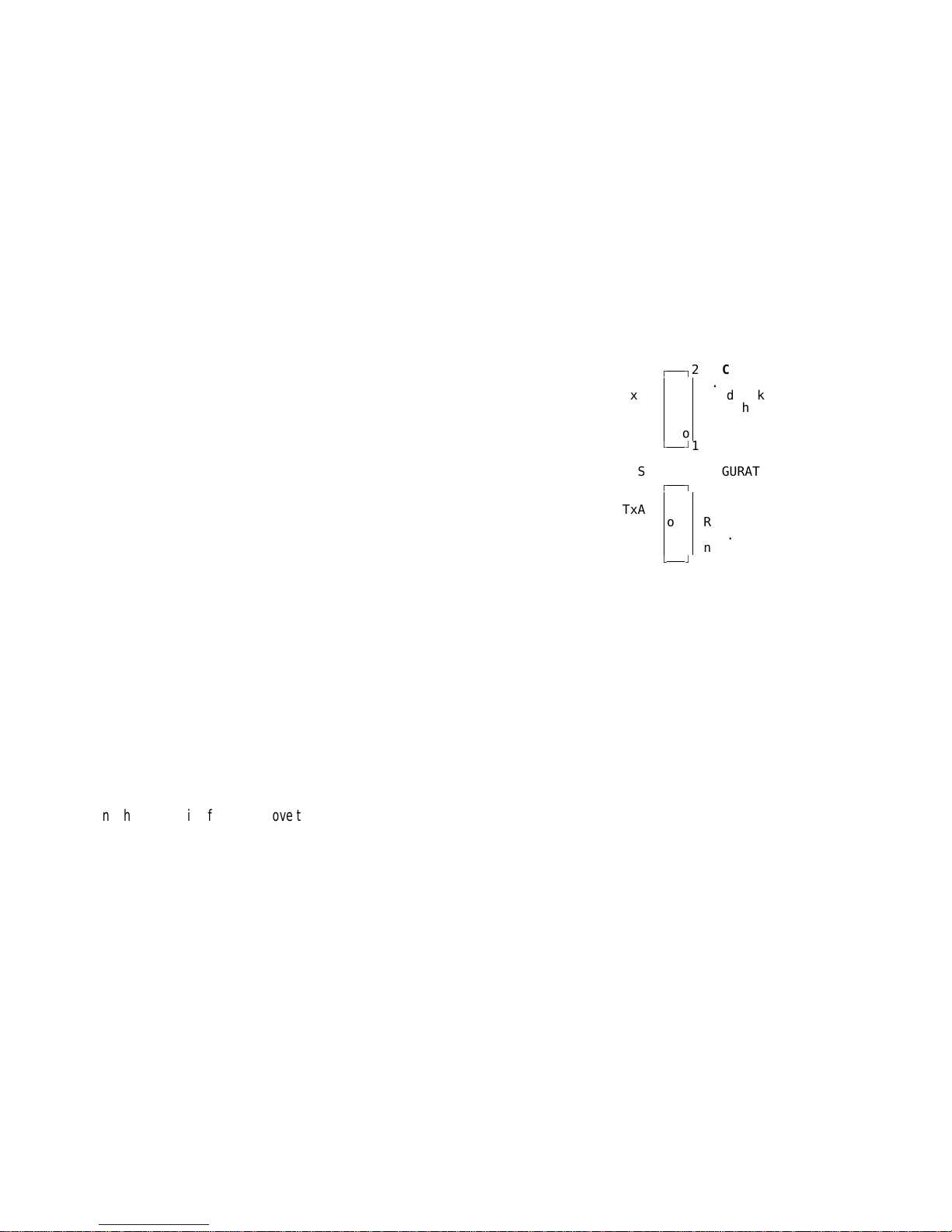
KEYPAD CN4
o Y5
1
o
X4
o
X3
o
X2
o
X1
o
Y4
o
Y3
o
Y2
o
Y1
o
GND
9
RETURN VALUES
X1 X2 X3 X4
00
01
02
03
Y1
04
05
06
07
Y2
08
09
0A
0B
Y3
0C
0D
0E
0F
Y4
10
11
12
13
Y5
CLR P5.1 ; ENABLE MMIO
SETB TCON.2 ; INT1 IS FALLING EDGE SENSITIVE
CLR IEN0.2 ; DISABLE INT1, FROM VECTORING (INT FLAG..
; STILL GETS SET ON FALLING EDGE THOUGH)
A subroutine may be written which waits for a key to be pressed and returns the value in A, like the following:
GETKEY: JNB TCON.3,GETKEY ; LOOP TILL TRANSITION SENSED
MOV DPH,KEYPORT ; POINT TO KEYPAD PORT
MOVX A,@DPTR ; GET THE KEY
ANL A,00011111B ; MASK OFF UNUSED BITS
CLR TCON.3 ; CLEAR INT1 EDGE FLAG
RET
DIGITAL TO ANALOG CONVERTER
The D/A converter has four channels of eight bit resolution with
0 to 5 volt analog output range. Writing to ports 10 to 13 hex will
write to channels A, B, C, and D respectively. Writing 0 to a port
causes 0V to be output and writing FF hex causes 5V to be
output.
+Vin is the unregulated DC that is applied to ST1 and PX9 is a
port line which can be programmed as a digital input or output,
or an interrupt line.
LCD INTERFACE
D/A HDR2
1
2
+VIN
o o
GND
VOUTA
o o
GND
VOUTB
o o
GND
VOUTC
o o
GND
VOUTD
o o
GND
PX9
o o
GND
11
12
The LCD interface allows the MicroPac to control OPTREX
and compatible LCD panels. The power for LED
backlighting may be turned on by setting OP7. The
contrast level may be controlled by a fixed resistor on the
MicroPac or by a remote potentiometer. See the
distribution disk's assembly language drivers for
programming examples.
LCD PANEL HDR5
1
2 VCC
o o
GND
RS
o o
CONTRAST
E
o o
R/W*
D1
o o
DO
D3
o o
D2
D5
o o
D4
D7
o o
D6
BACKLIGHT K
o o
BACKLIGHT A
15
16

6
DIGITAL I/O
PX00-PX17
These ports are bidirectional. When a 1 is written to a port line it is configured as a input/output
port. It is considered an output port because it is outputing a logical 1, yet as soon as it is
externally brought low by an input, reading this port will return a 0. When there is no input, or
when a 1 is applied externally, reading this port will return a 1. When a 0 is written to the port, it
outputs a 0, but now cannot be used as an input port. During the reset function all the port
latches of the 80535 have 1s written to them.
When PX00-PX17 are used as outputs they can drive 4 LS-TTL inputs. When changing the
state of an output bit (or bits), the following instructions should be used:
ANL,ORL,XRL,JBC,CPL,INC,DEC,DJNZ,
MOV Px.y,C (Move carry bit to bit Y of port X),
CLR Px.y (Clear bit Y of Port X),
SET Px.y (Set bit Y of Port X).
These instructions should be used because they read the latch of a line instead of the signal
being output (or input) to the line. This is important because if a load, such as the base of a
transistor, is connected to one of the output lines, reading this port with instructions which read
the line instead of the latch (such as MOV A,P4) will always return a 0 because of the base's low
voltage drop. Instructions such as MOV A,P4 should be used when the ports are input only.
(For more information, see section 3.1 of the SAB 80515/80535 Single-Chip Microcontroller
User's Manual included in the appendices)
PX18-PX23 and IP0, IP1
The remaining lines PX18-PX23 are supplied by the SC26C92, with OP2,OP3 and OP4 being
output only, and IP0, IP1, IP2, IP3 and IP6 being input only. The inputs IP0 and IP1 are on the
I/O Expansion Connector (discussed later). The SC26C92 inputs and outputs are defined as
follows:
DIGITAL I/O
HDR3
50 49
GND
o o
VCC
GND
o o
PX0 P4.0
GND
o o
PX1 P4.1
GND
o o
PX2 P4.2
GND
o o
PX3 P4.3
GND
o o
PX4 P4.4
GND
o o
PX5 P4.5
GND
o o
PX6 P4.6
GND
o o
PX7 P4.7
GND
o o
PX8 P1.O/INT3*/CC0
GND
o o
PX9 P1.1/INT4/CC1
GND
o o
PX10 P1.2/INT5/CC2
GND
o o
PX11 P1.3/INT6/CC3
GND
o o
PX12 P1.4/INT2*
GND
o o
PX13 P1.5/T2EX
GND
o o
PX14 P1.6/CLKOUT
GND
o o
PX15 P1.7/T2
GND
o o
PX16 P3.4/TO
GND
o o
PX17 P3.5/T1
GND
o o
PX18 OP2
GND
o o
PX19 IP2
GND
o o
PX20 OP3
GND
o o
PX21 IP3
GND
o o
PX22 OP4
GND
o o
PX23 IP6
2 1
OP2:General purpose output, or Channel A transmitter 1X or 16X clock output, or Channel A receiver 1X clock output.
OP3:General purpose output, or open-drain, active-low counter/timer output or Channel B transmitter 1X clock output or receiver 1X
output.
OP4:General purpose output, or open-drain, active-low RxRDYA/FFULLA
IP0:General purpose input, or Channel A clear to send active low input.
IP1:General purpose input, or Channel B clear to send active low input.
IP2:General purpose input, or counter/timer external clock input.
IP3:General purpose input, or Channel A transmitter external clock input (TxCA).
IP6:General purpose input, or Channel B receiver external clock input (RxCB).
Before using PX18-PX23 or any other function of the SC26C92, you must reset the chip as follows:
SETB P5.5 ; MAKE THE RESET LINE HIGH
CLR P5.5 ; THEN LOW

7
This will clear the following SC26C92 registers: SRA, SRB, IMR, ISR, OPR, and OPCR. It will also put OP0-OPT into the high state, stop
the counter/timer, and make channel A and B inactive with the TxDA and TxDB outputs in the high state.
After reset OP2-4 default as general purpose outputs. If after reset they have been programmed for another function they may be
programmed to outputs again by programming register OPCR (see data sheets). When these ports are configured as outputs they output
the complement of the data in OPR (an internal register of the SC26C92) which is controlled by the OUTSET and OUTRES ports.
For example, to make OP2 high we must make bit 2 of OPR low (since the complement of OPR is output). A 1 in any of the bits that are
written to the OUTRES port will result in the corresponding bit in OPR being brought low (reset), allowing you to selectively reset any or all
of the bits without affecting the others. The following code does this.
CLR P5.1 ; enable MMIO
MOV DPH,#OUTRES ; select OUTRES port
MOV A,#00000100B ; bit 2 of A is set
MOVX @DPTR,A ; write A to OUTRES, resetting bit 2 of OPR only
...subsequently writing the same value to OUTSET port will make OP2 high:
MOV DPH,#OUTSET ; select OUTSET port
MOVX @DPTR,A ; write A to OUTSET, setting bit 2 of OPR only
As shown above, OUTSET works the same as OUTRES except it selectively sets bits in OPR.
The inputs IP0, IP1, IP2, IP3 and IP6 may be programmed to be general purpose inputs; they are unlatched and may be examined by
simply reading the UARTIN port and examining bits 0,1,2,3 and 6. The inputs IP0-IP3 have a unique feature in that they can also detect a
change in state. This is defined as a high-to-low, or low-to-high input transition that lasts longer than 50 uS. When the IPCR port is read,
bits 0-3 will read the same as the corresponding bits in the UARTIN port, and bits 4-7 if set to 1 will indicate a change of state for IP0-IP3
respectively. After the port is read, bits 4-7 are automatically reset.
For more details on SC26C92 input and output, see the SC26C92 data sheets.
ANALOG INPUTS
The 8 channels of 8 bit A/D have a range of 0-5V. The upper end of this range is fine
tuned when the unit is built and may be adjusted using VR1 if it later gets out of spec. The
range defaults to 0-5V but the upper and lower range may be programmed to other values
(within a 0-5V range) by writing to the 80535 special function register DAPR (For more
information, see assembly language drivers and section 3.5 of the SAB 80515/80535
Single-Chip Microcontroller User's Manual included in the appendices)
You may select 1 of 8 channels to read the data from and when the conversion is finished,
read the data from register ADDAT. Below is a simple A/D conversion subroutine:
Analog Input HDR4
1
2
analog channel 0
o o
ANL GND
analog channel 1
o o
ANL GND
analog channel 2
o o
ANL GND
analog channel 3
o o
ANL GND
analog channel 4
o o
ANL GND
analog channel 5
o o
ANL GND
analog channel 6
o o
ANL GND
analog channel 7
o o
ANL GND
ground
o o
ground
+VIN
o o
VCC
19
20
; ADCIN
; Return ACC with the 8 bit A/D conversion from the channel selected by ACC
;
ADCIN:
ANL A,#111B ; ONLY 8 CHANNELS
ANL ADCON,#11000000B ; MODE FOR A/D CONVERSION: SINGLE
ORL ADCON,A ; "OR" IN THE CHANNEL
MOV DAPR,#0 ; START CONV W/NO REF VOLTAGE
JB BSY,$ ; LOOP TILL CONVERTED
MOV ACC,ADDAT ; ACC = CONVERSION
RET
8
SERIAL PORTS
The three serial ports may be individually configured for RS-232 or RS-422, and may be programmed for 8 or 9 bit protocol at standard
baud rates from 1200 to 19,200 for COM0 and 50 to 38400 for COM1 and COM2. Higher non-standard baud rates may be programmed
also.
The RS-422 option allows up to 32 serial ports to use the same twisted pair. Each end of the pair should have a terminating resistor that
matches the characteristic impedance of the line. Typically 33 ohms can be used.
The serial ports allow for multiprocessor communication using 9 bit protocol. This innovative function when enabled, will interrupt the
processor if the 9th bit of a data byte is set. Using the appropriate software allows for a powerful communication scheme.
COM0
This port is the 80535 serial interface which has 4 modes of operation. Since mode 0 is not
directly supported by the hardware, only modes 1, 2 and 3 will be described here.
MODE 1: 10 bits are transmitted or received: a start bit of 0, 8 data, and a stop bit
of 1. The baud rate is variable.
MODE 2: 11 bits are transmitted or received: a start bit of 0, 8 data, a
programmable 9th bit, and a stop bit of 1. When transmitting, the 9th bit
comes from TB8 in SCON. This could be used to hold the parity of the
data. When receiving, the 9th bit goes to RB8 in SCON, while the stop
bit is ignored. The baud rate can be either 1/32 or 1/64 of the oscillator
frequency
MODE 3: Same as mode 2 except the baud rate is variable.
For standard baud rates in modes 1 and 3 (using a 11.059 MHZ crystal), the overflow rate
of TIMER 1 and the setting of SMOD (PCON. 7) should be used to control the baud rate.
BAUD TIMER 1
RATE SMOD RELOAD VALUE
19200 1 FDH
9600 0 FDH
4800 0 FAH
2400 0 F4H
1200 0 E8H
(RS-232 CONFIGURATION)
1
2 CN1
n.c.
o o
n.c.
Tx
o o
handshake in (P5.7)
Rx
o o
handshake out (P5.6)
n.c.
o o
n.c.
GND
o o
n.c.
9
10
(RS-485 CONFIGURATION)
1
2 CN1
n.c.
o o
n.c.
TxA
o o
RxB
TxB
o o
RxA
n.c.
o o
n.c.
GND
o o
n.c.
9
10
Using the information from the above table, you can modify the subroutine SERST below to generate different baud rates:
;
; SERST - Serial port setup and start.
;
SERST:CLR SMOD ; Make SMOD = 0
MOV TH1,#0FDh ; Set up timer 1 for 9600 baud using
MOV TL0,#0FDh ; a 11.059 crystal
MOV TMOD,#20h
MOV TCON,#40h
MOV SCON,#52h ; MODE 1. Set transmit ready flag
RET
Serial I/O is really straightforward, as shown in the following subroutines:

9
;
; COM0IN: Return a char in ACC from COM0
;
COM0IN:
JNB RI,$ ; Wait for receiver flag.
CLR RI ; Clear receiver flag.
MOV A,SBUF ; Read character.
RET
;
; COM0OUT: Output the char in ACC to COM0
;
COM0OUT:
JNB TI,$ ; WAIT TILL BUFFER EMPTY
CLR TI ; CLEAR FLAG
MOV SBUF,A ; SEND THE CHAR
RET
For more information on this serial interface, see section 3.4 of the SAB 80515/80535 Single-Chip Microcontroller User's Manual included
in the appendices.
COM0 HANDSHAKE LINES
An input and output handshake line is available with the standard RS-232 option which allows you to implement software handshaking.
The input line is connected to P5.7 and you will read a 0 or 1 for a + or - RS-232 level, respectively (note that if 0 has been written to P5.7,
1 must be written to it to make it an input). The output line is connected to P5.6, and similarly a 0 or 1 output will produce a + or - RS-232
level, respectively.
When the RS-422 option is installed, an output of 1 on P5.6 enables the transmitter and a 0 disables.
COM1 AND COM2
These ports are in the SC26C92 with COM1 and COM2 corresponding to channel A and
channel B respectively. The ports are very versatile as seen in the following list of features:
Quadruple buffered receiver data registers
Programmable data format
5 to 8 data bits plus parity
odd, even, no parity or force parity
1, 1.5 or 2 stop bits programmable in 1/16-bit increments
Programmable baud rate for each receiver and transmitter selectable from:
18 fixed rates: 50 to 38400 baud
non-standard rates to 115200 baud
one user defined rate derived from programmable timer/counter
external 1X or 16X clock
Parity, framing, and overrun error detection
False start bit detection
Line break, and mid character break detection
Programmable channel mode
Normal (full-duplex)
Automatic echo
Local loopback
Remote loopback
Automatic wake-up mode for multidrop applications
(RS-232 CONFIGURATION)
COM1 (CHANNEL A)
1
2 CN2
n.c.
o o
n.c.
Tx
o o
handshake in (IP4)
Rx
o o
handshake out (OP0)
n.c.
o o
n.c.
GND
o o
n.c.
9
10
COM2 (CHANNEL B)
1
2 CN3
n.c.
o o
n.c.
Tx
o o
handshake in (IP5)
Rx
o o
handshake out (OP1)
n.c.
o o
n.c.
GND
o o
n.c.
9
10
(RS-485 CONFIGURATION)
CN2 & CN3
1
2
n.c.
o o
n.c.
TxA
o o
RxB
TxB
o o
RxA
n.c.
o o
n.c.
GND
o o
n.c.
9
10

10
COM1, COM2 HANDSHAKE LINES
The RS-232 configuration provides handshake inputs for COM1 and COM2 which may be examined by reading IP4 and IP5 respectively.
Reading a 0 is a + RS-232 input and 1 is a - RS-232 input. AIso in this configuration, OP0 and OP1 control the handshake outputs for
COM1 and COM2 respectively. Normally these are controlled by using the OUTSET and OUTRES commands, but setting bit 5 of MR2A
(for COM1) or MR2B (for COM2) will enable the Request-to Send (RTS) function. When enabled, this function will bring the corresponding
handshake out line to a - RS-232 level one bit time after the characters in the Channel A (or B for COM2) transmit shift register and in the
THR, if any, are completely transmitted including the programmed number of stop bits, if the transmitter is not enabled. To automatically
terminate a string of characters, do the following:
Enable the RTS function
Enable the transmitter
Set handshake out line to + RS-232 level using the OUTSET command
Send string, and immediately after writing last character to THR, disable transmitter
The last character will be sent and the handshake out line will go to a - RS-232 level one bit time afterward.
In the RS-422 configuration OP0 and OP1 are used to enable the transmitters for COM1 and COM2 respectively. Use the OUTRES
command to enable and OUTSET to disable.
Because of the may features of the chip, initialization is a bit more complicated as you can see from the following subroutine.
;
; INIT2681: SET UP COM1 AND COM2 FOR NO PARITY, ONE STOP BIT AND 8 DATA
; AT 9600 BAUD.
;
MR1ADAT EQU 00010011B ; no RTS, Rx int on RxRDY, char mode, no parity, 8 data
MR2ADAT EQU 00000111B ; normal,no TxRTS, no CTS, 1 stop bit
MR1BDAT EQU 00010011B ; no RTS, Rx int on RxRDY, char mode, no parity, 8 data
MR2BDAT EQU 00000111B ; normal,no TxRTS, no CTS, 1 stop bit
INIT2681:
; DO RESET COMMANDS FOR PORTS A AND B. THIS WILL EXECUTE CHANNEL
; A & B's MISCELLANEOUS COMMANDS NUMBERED 101,100,011,010,001.
MOV A,#01010000B ; DO FROM THIS COMMAND, DOWN TO 00010000
CRINIT: MOV P2,#CRA
MOVX @R1,A
MOV P2,#CRB
MOVX @R1,A
ADD A,#-16 ; SUBTRACT 1 FROM UPPER NIBBLE
JNZ CRINIT ; LOOP TILL 0
MOV P2,#MR1A ; SETUP PROTOCOL FOR PORT A
MOV A,#MR1ADAT
MOVX @R1,A
MOV A,#MR2ADAT
MOVX @R1,A
MOV P2,#MR1B ; SETUP PROTOCOL FOR PORT B
MOV A,#MR1BDAT
MOVX @R1,A
MOV A,#MR2BDAT
MOVX @R1,A
; SELECT BAUD RATE
MOV P2,#ACR
MOV A,#80H
MOVX @R1,A ; SELECT SET 2 OF BAUD RATES
MOV P2,#CSRA
MOV A,#10111011B
MOVX @R1,A ; RX AND TX AT 9600 FOR A
MOV P2,#CSRB
MOVX @R1,A ; RX AND TX AT 9600 FOR B
continued on next page....

11
MOV P2,#CRA
MOV A,#00000101B ; ENABLE TXER AND RXER
MOVX @R1,A
MOV P2,#CRB
MOVX @R1,A ; SAME FOR B
RET
The following input and output routines are simpler, as you can see.
;
; Serial port A input
;
SERINA:
MOV P2,#SRA
SERINA1: MOVX A,@R1
JNB ACC.0,SERINA1 ; LOOP TILL RXrdy
MOV P2,#RHRA ; READ DATA PORT
MOVX A,@R1
RET
;
; Serial port B input
;
SERINB:
MOV P2,#SRB
SERINB1: MOVX A,@R1
JNB ACC.0,SERINB1 ; LOOP TILL RXrdy
MOV P2,#RHRB ; READ DATA PORT
MOVX A,@R1
RET
;
;Serial port A output
;
SEROUTA:
MOV P2,#SRA
PUSH ACC ; SAVE CHAR
SOUTA1: MOVX A,@R1
JNB ACC.2,SOUTA1 ; LOOP TILL TXrdy
POP ACC
MOV P2,#THRA ; SEND IT OUT
MOVX @R1,A
RET
;
;Serial port B output
;
SEROUTB:
MOV P2,#SRB
PUSH ACC ; SAVE CHAR
SOUTB1: MOVX A,@R1
JNB ACC.2,SOUTB1 ; LOOP TILL TXrdy
POP ACC
MOV P2,#THRB ; SEND IT OUT
MOVX @R1,A
RET
For more details, see the SC26C92 data sheets.

12
TIMER/COUNTERS
TIMER 0 AND TIMER 1
These timers are each 16 bits and can be programmed individually to be in counter or timer
mode, in addition to 4 different modes of operation. Note when using mode 0 that INT1 is used
by the keypad circuit and will have a high normally applied to it, and a low when a key is
pressed.
When using counter mode for TIMER 0 the signal is input through P3.4/T0, or for TIMER 1,
through P3.5/T1. These pins as well as P1.5/T2EX, P1.7/T2, CCO, CC1, CC2 and CC3 must
be configured as inputs by writing 1 to them if their default settings have been changed.
TIMER 2
This 16 bit timer is also referred to as PTRA Unit (Programmable Timer/Counter Register Array)
which can be used as a timer, event counter, or gated timer. In each configuration an interrupt
may be generated on counter overflow. The counter input signal (or, in gated timer mode, the
timer gate) comes from P1.7/T2.
Once the timer or counter function has been enabled, 3 other modes of operation may be
selected: reload, compare, and capture.
By default, when TH2 and TL2 are incremented above FFFFh, they roll over to 0000. In reload
mode 1, TH2 and TL2 are loaded with the values stored in CRCH and CRCL respectively, on a
falling edge of P1.5/T2EX. In reload mode 0, these values are loaded when the timer rolls over.
Compare mode is used to provide 4 PWM (pulse width modulated) output signals with 16 bits of
resolution from the CC0, CC1, CC2 and CC3 lines.
DIGITAL I/O
HDR3
50 49
GND
o o
VCC
GND
o o
PX0 P4.0
GND
o o
PX1 P4.1
GND
o o
PX2 P4.2
GND
o o
PX3 P4.3
GND
o o
PX4 P4.4
GND
o o
PX5 P4.5
GND
o o
PX6 P4.6
GND
o o
PX7 P4.7
GND
o o
PX8 P1.O/INT3*/CC0
GND
o o
PX9 P1.1/INT4/CC1
GND
o o
PX10 P1.2/INT5/CC2
GND
o o
PX11 P1.3/INT6/CC3
GND
o o
PX12 P1.4/INT2*
GND
o o
PX13 P1.5/T2EX
GND
o o
PX14 P1.6/CLKOUT
GND
o o
PX15 P1.7/T2
GND
o o
PX16 P3.4/TO
GND
o o
PX17 P3.5/T1
GND
o o
PX18 OP2
GND
o o
PX19 IP2
GND
o o
PX20 OP3
GND
o o
PX21 IP3
GND
o o
PX22 OP4
GND
o o
PX23 IP6
2 1
Capture mode 0 can be used to decode 4 PWM signals with 16 bits of resolution again, using the CC0, CC1, CC2 and CC3 lines as
capture input signals (remember, P1.0-1.3 must be configured as inputs). Capture mode 1 can be used to read timer 2 while it is running
to eliminate the problem of a wrong reading caused by a rollover occurring between the time of reading the lower and upper byte of the
timer.
For details on programming, see section 3.2 and 3.3 of the SAB 80515/80535 Single-Chip Microcontroller User's Manual included in the
appendices.
C/T
The designation C/T is used in the SC26C92 data sheets, to refer to the Counter/Timer. This C/T counts down instead of up as with the
other timer/counters. The minimum count that can be loaded into the C/T is 0002h. The terms counter (which commonly refers to a device
that produces an output based on the number of external signals received) and timer (which refers to a device with a programmable output
based on a constant clock source) are used differently in the data sheets. What they refer to as timer mode shares features of a counter,
and vice-versa. For example, there are 2 timer modes which use an external input (IP2) to clock the timer. Though this may be confusing,
we will follow their definitions.
In timer mode, a square wave output will be produced which has a period of 2 * (value loaded into C/T registers) * (period of clock source).
This output will set the Counter Ready interrupt flag (ISR[3]) each period (this flag is reset by the STOPCNT command, without stopping
the timer), and if OPCR[3]=0 and OPCR[2]=1 the square wave will be output on OP3.
In counter mode the C/T is enabled to decrement the value loaded into it after the STRTCNT command, and upon reaching 0000 the
Counter Ready interrupt flag (ISR[3]) is set and the counter will continue to decrement until a STOPCNT command, which also clears the
interrupt flag. If OP3 is programmed to be a C/T output, it will remain high until it reaches the terminal count and goes low. The output
goes high again after a STOPCNT command (see the SC26C92 data sheets for more details).

13
SIGNAL OUTPUTS
For applications that need a signal output, there are 3 sources available:
CLOCKOUT this can be programmed to provide a system clock output of 1/12 the oscillator frequency.
OP2 this can output channel A's transmitter clock, transmitter clock times 16, or receiver clock.
OP3 this can output channel B's transmitter clock, receiver clock, or the C/T output
WATCHDOG TIMER
The watchdog timer is built into the SAB 80535 processor and is used to reset the MicroPac 535 in the event that a hardware or software
crash occurs. When the watchdog timer is enabled the software must clear the timer at least once every 65532 machine cycles (a
machine cycle is 1/12 of the oscillator frequency), otherwise a reset will occur. This reset is the same as an external reset, except that bit
WDTS (bit 6 of IP0) is set. Using this, the software can determine the source of the reset.
To enable the watchdog timer (it is disabled by default), set the SWDT bit which is bit 6 of IEN1. Once it has been enabled, the only way it
can be disabled is through an external reset. Once it is enabled, to clear the timer you must set the WDT bit (IEN0.6) and then the SWDT
bit. The requirement of setting two bits independently lessens the possibility of a crashing program from clearing the watchdog timer. See
also section 3.7 of the SAB 80515/80535 Single-Chip Microcontroller User's Manual included in the appendices.
INTERRUPTS
The 80535 has 5 internal interrupt sources and 7 external sources, and the SC26C92 has a
single interrupt output with eight maskable interrupt sources. As these devices are configured
on the MicroPac 535, this works out to 9 external interrupt sources (10 available when timer 2
reload mode is disabled) and 9 on-board. The external interrupts IP0 and IP1 are available on
the expansion connector (the connector is discussed later) and the rest are all available on
HDR3. For more information on 80535 interrupts, see section 3.6 of the SAB 80515/80535
Single-Chip Microcontroller User's Manual included in the appendices. The interrupt sources are
as follows:
EXTERNAL
INT2* (programmable for rising or falling edge trigger)
INT3* (programmable for rising or falling edge trigger)
INT4 (rising edge triggered)
INT5 (rising edge triggered)
INT6 (rising edge triggered)
T2EX/P1.5 (when timer 2 reload mode is disabled, it is falling edge triggered)
Through INT0/P3.2 the following SC26C92 interrupts are detected:
IP0 (rising AND falling edge triggered)
IP1 (rising AND falling edge triggered)
IP2 (rising AND falling edge triggered)
IP3 (rising AND falling edge triggered)
INTERNAL
A/D Convertor
Timer 0
Timer 1
Timer 2
COM0 (80535 serial port)
INT1/P3.3 (keypad)
EXTERNAL
DIGITAL I/O
HDR3
50 49
GND
o o
VCC
GND
o o
PX0 P4.0
GND
o o
PX1 P4.1
GND
o o
PX2 P4.2
GND
o o
PX3 P4.3
GND
o o
PX4 P4.4
GND
o o
PX5 P4.5
GND
o o
PX6 P4.6
GND
o o
PX7 P4.7
GND
o o
PX8 P1.O/INT3*/CC0
GND
o o
PX9 P1.1/INT4/CC1
GND
o o
PX10 P1.2/INT5/CC2
GND
o o
PX11 P1.3/INT6/CC3
GND
o o
PX12 P1.4/INT2*
GND
o o
PX13 P1.5/T2EX
GND
o o
PX14 P1.6/CLKOUT
GND
o o
PX15 P1.7/T2
GND
o o
PX16 P3.4/TO
GND
o o
PX17 P3.5/T1
GND
o o
PX18 OP2
GND
o o
PX19 IP2
GND
o o
PX20 OP3
GND
o o
PX21 IP3
GND
o o
PX22 OP4
GND
o o
PX23 IP6
2 1
14
Through INT0/P3.2 the following SC26C92 interrupts are detected:
COM1 (channel A)
COM2 (channel B)
Counter Ready
SC26C92 INTERRUPTS
All of the SC26C92 interrupts (internal and external) are detected by the 80535's INT0/P3.2 input and it is suggested that INT0 be set up
as low level triggered. To enable SC26C92 interrupts you must first select which of its interrupts will be enabled by setting the
corresponding bits in the IMR port. After this you must set bits EAL and EX0 of IEN0. All interrupts are globally disabled unless EAL is
set, and setting EX0 enables INT0. Now any SC26C92 interrupt will cause an INT0 interrupt.
When an INT0 interrupt occurs, its interrupt handler must find the source or sources of the SC26C92 interrupt. When there is only 1
enabled, you know that the source is the interrupt that is enabled, but if more than 1 is enabled, some extra code is needed in the handler
to vector to the various SC26C92 device handlers.
Since the ISR port can indicate pending interrupts even when the interrupts are masked off by IMR, we want to determine which of the
devices have both an ISR bit set and a corresponding IMR bit set. This may be done by logically ANDing the value read from the ISR port
with the value written to the IMR port (since IMR is write only, the value written to it must be a constant or must be stored in a memory
location to be retrieved by the interrupt handler). Once the sources have been determined, the INT0 handler must vector to each of the
corresponding SC26C92 device handlers.
The SC26C92 can be programmed to generate interrupts when a change of state occurs on any of the IP0-IP3 inputs. See Digital I/O
section for description of change of state, and see the SC26C92 data sheets for detailed information interrupts and associated registers.
EXPANSION CONNECTOR
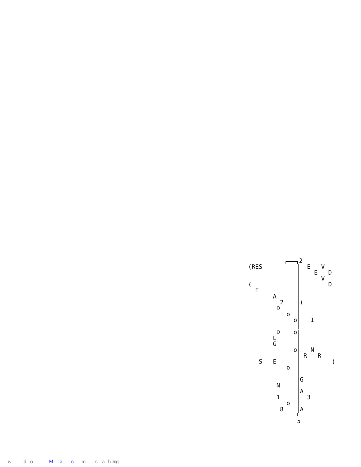
This connector allows connection to EMAC peripherals, as well as peripherals of your own
design. Included are:
AD0-AD7 8 bit data bus
A8-A15 upper byte of the address bus
EXTIO* external I/O select line which is asserted low when P2 contains a value from
70 to 7F and P5.1=0 (MMIO enabled), providing up to 16 external I/O ports.
See section on Memory Mapped I/O.
WR* active low write select line
RD* active low read select line
RESET active high RESET controlled by P5.5
INT0, INT1 These are the SC26C92 IP0 and IP1 inputs respectively which can be
programmed as general purpose inputs, UART CTS's, or interrupts that are
triggered on both the rising and falling edge of an input. These pins are not
to be confused with the 80535's pins of the same name. These names were
used for compatibility with existing EMAC peripherals.
GND, +VIN These provide ground and the voltage supplied to pin 1 of ST1. There is
also a 10k pullup to Vcc available.
The reserved pins are not connected on this revision of the MicroPac 535 but may in future
revisions, so to maintain compatibility they should be left unconnected in peripherals of your own
design.
I/O EXPANSION CONNECTOR
HDR1
1
2
(RESERVED)
o o
(RESERVED)
(RESERVED)
o o
(RESERVED)
(RESERVED)
o o
(RESERVED)
(RESERVED)
o o
(RESERVED)
(RESERVED)
o o
(RESERVED)
AD1
o o
AD0
AD2
o o
(RESERVED)
AD3
o o
INT1 (IP1)
AD4
o o
INT0 (IP0)
AD5
o o
EXTIO*
AD6
o o
RESET
AD7
o o
WR*
VCC PULLUP
o o
RD*
GND
o o
GND
+VIN
o o
+VIN
(RESERVED)
o o
(RESERVED)
(RESERVED)
o o
(RESERVED)
GND
o o
GND
GND
o o
GND
GND
o o
GND
GND
o o
GND
A14
o o
A15
A12
o o
A13
A10
o o
A11
A8
o o
A9
49 50

APPENDIX A
SAB 80515/80535
Single-Chip Microcontroller
User's Manual
Reprinted with permission from Siemens Components, Inc.
Copyright Siemens Components, Inc.

APPENDIX B
SC26C92 Programming and
Data Reference Sheets
Reprinted with permission from Philips Semiconductors
Copyright Philips Semiconductors
Table of contents
Other EMAC Motherboard manuals


