Enpirion EV1340QI User manual

EV1340QI Evaluation Board User Guide
March 2012
Page 1 of 7
Enpirion EV1340QI 5A DC/DC
Converter with Integrated Inductor
Evaluation Board
Introduction
Thank you for choosing Enpirion, the source for Ultra small foot print power
converter products. This user guide is applicable to evaluation boards with part
number 05043 Rev A shown on the back side of the PCB. Along with this
document you will also need the latest device datasheet.
•The EV1340QI features integrated inductor, power MOSFETS, Controller,
bulk of the compensation Network, and protection circuitry against system
faults. This level of integration delivers a substantial reduction in footprint
and part count over competing solutions. The evaluation board is
optimized for ease of use.
•The EV1340QI features a customer programmable output voltage by
means of a resistor divider. This evaluation board, as shipped is populated
with one option for VOUT. It is programmed so that VOUT will be half of
VDDQ.
•The EV1340QI includes the bulk of the compensation network internally.
However, an external phase-lead (zero) capacitor and resistor is required
in addition to two resistor dividers to set the output voltage. This network is
shown in Figure -1. Appropriate component values allow for optimum
compensation for a given VDDQ voltage and choice of loop bandwidth.
The values in Figure 1 are as populated on the eval board, and have been
optimized for VDDQ = 1.5V. The circuit in Figure 1 will be stable for lower
values of VDDQ as well. For VDDQ higher than 1.5V, please see the
datasheet to calculate the resistor divider and compensation values.
•Jumpers or test points are provided for ease of logical 1/0 programming of
the following signals:
oENABLE (ENA)
oEN_PB input
ENABLE may also be controlled using an external switching source by
removing the jumper and applying the enable signal to the middle pin and
ground.
•The board comes with input decoupling and reverse polarity protection to
guard the device against common setup mishaps.
Downloaded from Elcodis.com electronic components distributor

EV1340QI Evaluation Board User Guide
March 2012
Page 2 of 7
Figure 1: Output voltage programming and loop compensation
Quick Start Guide
Figure 2: J2 allows control of the Enable pin.
The jumper on Enable pin as shown is in disable mode. When jumper is between
the middle and right pins the signal pin is connected to ground or logic low. When
the jumper is between the left and middle pins, the signal pin is connected to
AVIN or logic High.
WARNING: complete steps 1 through 6 before applying power to the EV1340QI
evaluation board.
STEP 1: Set the “ENA” jumper to the Disable Position. See Figure 2 above.
STEP 2: Set the EN_PB jumper J1 to the desired position. See Figure 3. Pulling
it low disables the pre-bias mode operation. Pulling this jumper high or
letting it float will allow monotonic start-up with a pre-biased output. In
pre-bias mode, VOUT will not discharge very quickly. Therefore, you
may need to apply a small load (~10mA) at shut-down to ensure that
the output voltage discharges. In Figure 3 the jumper is set low to
disable pre-bias mode.
Figure 3: J1 controls EN_PB input.
VIN
SIDE
GND
SIDE
VDDQ.ofhalf
bewillVcircuit,With this
**V
01.3,33
604,150
10,15
OUT
OUT
1
B
BA
DC
D
A
BA
DC
RRR
RR R
VDDQ
kRpFC
kRkR
kRkR
+
+
=
Ω==
Ω=Ω=
Ω
=Ω
=
Downloaded from Elcodis.com electronic components distributor

EV1340QI Evaluation Board User Guide
March 2012
Page 3 of 7
CAUTION:Except ENA, no other jumpers can be changed while the
EV1340QI is powered on. Doing so could result in damage to the part.
STEP 4: Connect the VDDQ Power Supply to the input power connectors,
VDDQ (J13) and GND (J7) as indicated in Figure 4 and set the power
supply to the desired voltage (≤1.8V). For VDDQ more than 1.5V, the
loop compensation values will have to be adjusted according to the
datasheet.
CAUTION:Be mindful of the polarity and magnitude. Even though the
evaluation board comes with reverse polarity protection diodes, it may not
protect the device for all conditions.
STEP 5: Connect AVIN power supply to the input connectors AVIN (J15) and
GND (J7) as indicated in Figure 4 and set the power supply to the
desired voltage (3.3V nominal).
CAUTION:The AVIN power connection on this board has no reverse
polarity or voltage clamping protection on it.
STEP 6: Connect the load to the output connectors VOUT (J4) and GND (J6),
as indicated in Figure 4.
STEP 7: Power up the board by turning on the AVIN power supply first and then
the VDDQ supply. Next, move the ENA jumper to the enabled position.
The EV1340QI is now powered up and VOUT should be half of VDDQ.
You are free to make Efficiency, Ripple, Line/Load Regulation, Load
transient, Power OK, and temperature related measurements.
STEP 7A: Power Up/Down Behavior – Remove ENA jumper and connect a
pulse generator (output disabled) signal to the middle pin of ENA and Ground.
Set the pulse amplitude to swing from 0 to 2.5 volts. Set the pulse period to
10msec, duty cycle to 50% and fast transition (<1usec.) Hook up oscilloscope
probes to ENA, POK and VOUT with clean ground returns. Enable pulse generator
output. Observe the VOUT voltage ramps as ENA goes high and again as ENA
goes low.
STEP 8: You can also operate the board by leaving the ENA jumper in the high
position. Then apply AVIN to the board. Next, turn on the VDDQ
supply. The output will ramp up and down as half of VDDQ all the time.
CAUTION:If the device is powered up into a short-circuit condition, it is
susceptible to damage. Customers are advised to limit the VDDQ power supply
compliance to an acceptable level to mitigate this issue.
ALWAYS power down device before changing any board level components!
Downloaded from Elcodis.com electronic components distributor


EV1340QI Evaluation Board User Guide
March 2012
Page 5 of 7
Figure 5: Evaluation Board Schematic
Short across R9
when all other
routing completed
TP5
TP1
0805
AVIN
0805
C22
0805 0805
0402
0402
0402
TP20
TP23
R6
R3
VDDQ
C7
J1
1
2
3
J2
1
2
3
TP2
C3
VDDQOK
EAOUT
EAOUT VFB2
p2 CJR11/12/2010J1, J2 were SMT. Added TP30-31.
R9 C4
TP30
TP31 C12
TP6
AVIN
AVIN
C13
TP32
TP33
TP34
TP35
12/14/2010p3 Added TP32-35, D4 CJR
TP16
D4
1206
1206
D1
Anode
Anode
D1 is MELF
D4 is MELF/SOT23
(alternate location)
J15
AVIN
0805
J13
VDDQ
VOUT
GND
R12
U1
EV1340QI
NC1
1
NC2
2
NC3
3
NC4
4
NC5
5
NC6
6
NC7
7
NC8
8
NC9
9
VOUT
10
VOUT
11
VOUT
12
VOUT
13
VOUT
14
VOUT
15
VOUT
16
VOUT
17
NC18
18
SW
19
SW
20
PGND
21
PGND
22
PGND
23
PGND
24
PGND
25
PGND
26
PGND
27
NC36 36
NC35 35
NC34 34
AVIN2 33
AGND2 32
VDDQ 31
VDDQ 30
VDDQ 29
VDDQ 28
NC54 54
NC53 53
NC(SW)52 52
NC(SW)51 51
NC(SW)50 50
NC(SW)49 49
VDDQOK 48
FQADJ 47
EN_PB 46
VSENSE 45
VREF 44
EAOUT 43
VFB 42
POK 41
AGND1 40
AVIN1 39
ENABLE 38
NC37 37
CONFIDENTIAL
Title
Size Drawing Number
Date
Rev
Sheet of
Drawn By
Rev ision Description Date Approved
R1
TP7
R15
J4
J7
1206
1206
1206
1206
C1
FB1
0805
0805
0805
R8
0805
0805
08050805
J6
VOUT
ENA
TP19
TP24
TP12
VDDQPGND
ENA
TP13
VOUT
POK
PGND
C2
TP14
0805
0805
0402
C6
TP15
R10
+
C35
C5
D3
S2A
0402
VDDQ
GND
C14
VFB2
VFB2
R11
EN_PB
TP3
R14
0805
EN_PB
TP4
FADJ
VREF
0805
0805
TP28
TP29
SCH 05042
PCB 05043
10/6/2010 CJRp1 Preliminary Release
C9
C17
C11
C8
C10
TP27
1
2
TP26
1
2
R7
VDDQ
0805
VOUT
C20
R2
0805
C19 C21
0402
TP9TP8
D2
TP25
BF_IN
C. Romano
0805
05042 EV1340 Engineering Board Schematic
TP21
1
2
TP22
1
2
R13
TP17 TP18
TP10 TP11
Downloaded from Elcodis.com electronic components distributor

EV1340QI Evaluation Board User Guide
March 2012
Page 6 of 7
Test Recommendations
To guarantee measurement accuracy, the following precautions should be
observed:
1. Make all input and output voltage measurements at the board using
the surface mount test points TP19, TP20, TP23, and TP24 provided.
This will eliminate voltage drop across the line and load cables that
can produce false readings.
2. Measure input and output current with calibrated series ammeters or
accurate shunt resistors. This is especially important for measuring
efficiency.
3. Use a low-loop-inductance probe tip similar to one shown below to
measure VOUT and switching signals to avoid noise coupling into the
probe ground lead. Output ripple and load transient deviations are
conveniently measured at TP27. For more accurate ripple
measurement, please refer to Enpirion App Note regarding this
subject.
4. The board includes a pull-up for the POK signal and ready to monitor
the power OK status.
5. A soft-start capacitor is populated on the board to provide a
reasonable soft-start time. It can be changed as needed.
Input and Output Capacitors
Please refer to the BOM section for the value of input caps and output caps used
on this evaluation board. Capacitors must be X5R or X7R dielectric formulations
to ensure adequate capacitance over operating voltage and temperature ranges.
Downloaded from Elcodis.com electronic components distributor
EV1340QI Evaluation Board User Guide
March 2012
Page 7 of 7
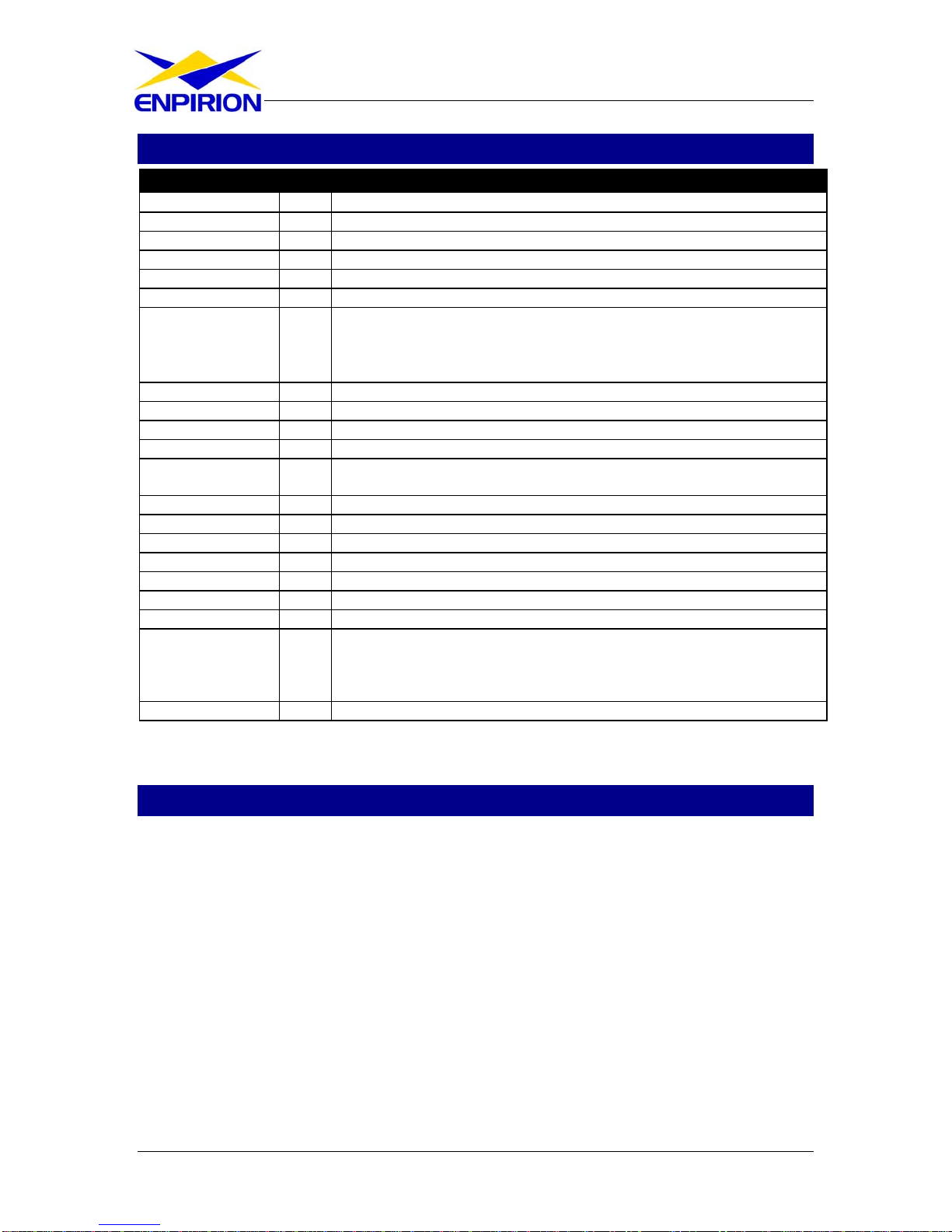
Bill of Materials
Designator Qty Description
C1, C19−C22 5 CAP, 10uF 0805 X7R 10% 10V CERAMIC
C2 1 CAP, 3300pF 5% 50V 0805 C0G
C5 1 CAP CERAMIC 33PF 50V NP0 0805
C8, C10 2 CAP, CER 100UF 6.3V X5R 1206
C9 1 CAP, CER 47UF 6.3V X5R 0805
C35 1 CAP, SMT ELECTROLYTIC, 150UF, 20%, 10V
C3, C4, C6, C7,
C11−C14, C17,
D4, R8, R9,
R13−R15
15
NOT USED
D1 1 DIODE SCHOTTKY 1A 40V MELF, TMBYV10-40FILM
D2, D3 2 S2A DIODE
FB1 1 SMT FERRITE BEAD 4A 0805, WURTH ELECTRONIK 742792012
J1,J2 3 CONN HEADER, VERTICAL, 3 POSITION, 0.100”, TIN
J4, J6, J7, J13,
J15 5 BANANA JACK, KEYSTONE 575-4
R1, R2 2 RES 100K OHM 1/16W 1% 0402 SMD
R3 1 RES 1/10W 15K OHM 0.1% 0805
R6 1 RES 10 K OHM 1/8W 0.1% 0805 SMD
R7 1 RES 3.57K OHM 1/8W 1% 0805 SMD
R10 1 RES 150K OHM 1/8W 0.1% 0805 SMD
R11 1 RES 3.01K OHM 1/8W 1% 0805 SMD
R12 1 RES 604K OHM 1/8W 0.1% 0805 SMD
TP1-TP5, TP16,
TP19, TP20,
TP23-TP25,
TP28-TP35
19
TEST POINT SURFACE MOUNT, KEYSTONE 5016
U1 1 EV1340QI QFN 5A
Contact Information
Enpirion, Inc.
Perryville III Corporate Park
53 Frontage Road - Suite 210
Hampton, NJ 08827 USA
Phone: 1.908.894.6000
Fax: 1.908.894.6090
Enpirion reserves the right to make changes in circuit design and/or specifications at any time
without notice. Information furnished by Enpirion is believed to be accurate and reliable. Enpirion
assumes no responsibility for its use or for infringement of patents or other third party rights,
which may result from its use. Enpirion products are not authorized for use in nuclear control
systems, as critical components in life support systems or equipment used in hazardous
environment without the express written authority from Enpirion.
Downloaded from Elcodis.com electronic components distributor
Table of contents
Other Enpirion Motherboard manuals


