Enpirion EN5339QI User manual

February 2012 R1.0
Page 1 of 8
Enpirion 2012 all rights reserved, E&OE www.enpirion.com
EN5339QI 3A Synchronous DCDC Converter
Evaluation
Board User Guide
Introduction
Thank you for choosing Enpirion, the source for ultra small foot print power converter products that
offer true ease of design with no compromise on performance.
You are evaluating Enpirion’s EN5339QI low profile 3A PowerSoC. The device is a fully integrated
step down DCDC converter with control/compensation, gate drive, MOSFET switches and Enpirion’s
proprietary high performance magnetics. It comes in a 4mm x 6mm x 1.1mm low profile package and
requires only a small number of external components to make a complete converter solution.
.
This user guide should be used together with the latest device datasheet. The datasheet can be
found at www.enpirion.com.
Following are the features of this evaluation board.
•Populated with one EN5339QI 3A PowerSoC with integrated inductor.
•Pre-tinned pads are available for a wide range of input and output capacitor configurations.
•There are four positions available for the output capacitors. The first position, closest to the IC,
can accommodate a 1206 or 0805 case size while the other three positions can accommodate
either 0805 or 0603 capacitor case sizes.
•The base output capacitor configuration is 3 x 22uF 0805 MLCC. Refer to the product
datasheet for output capacitor requirements.
•There are two positions for the input capacitors which can accommodate either 0805 or 0603
case sizes. The base input capacitor configuration is a single 22uF 0805 MLCC. Refer to the
product datasheet for input capacitor requirements.
•Output voltage programming is accomplished via a simple resistor divider. Jumpers are
provided for 4 pre-configured output settings. These settings are as follows:
•1.0V, 1.2V, 1.5V, 1.8V
•Easy jumpers are provided for the following signals:
•Enable
•Numerous test points are provided as well as clip leads for input and output connections
•The board comes with input decoupling and reverse polarity protection.

February 2012 R1.0
Page 2 of 8
Enpirion 2012 all rights reserved, E&OE www.enpirion.com
Quick Start Guide
Figure 1 shows a photograph of the evaluation board. Please refer to this figure while configuring the
board for evaluation.
STEP 1: Set the “ENABLE” jumper to the Disable Position.
STEP 2: Select the desired VOUT voltage setting by placing the jumper J2 on the correct jumper pin.
Below shows the VOUT jumper options.
CAUTION: the VOUT jumper settings can only be changed when the device is disabled.
Failure to follow this guideline may result in damage to the part.
STEP 3: Connect the Power Supply to the input power connectors, VIN (+) and GND (-). DO NOT
turn the power supply on yet.
CAUTION: be mindful of the polarity. Reversing polarity will result in damage to the part.
STEP 4: Connect an electronic load, or load board to the load to the output connectors VOUT (+) and
GND (-).
STEP 5: Power up the board and move the ENABLE jumper to the enabled position. The EN5339QI
is now powered up.
DISABLEENABLE

February 2012 R1.0
Page 3 of 8
Enpirion 2012 all rights reserved, E&OE www.enpirion.com
Figure 1. Evaluation Board top view.
Output Voltage Select
The EN5339QI is programmed via an external resistor divider. Figure 2 shows the device application
circuit.
EN5339
VOUT
PVIN
AGND
VIN
POK
ENABLE
AVIN PGND
CIN COUT
1 uF
VOUT
PGND
RPOK
Ra
Rb
VFB
POK
Ca
Figure 2. EN5339QI application Circuit.
J2 VOUT Jumpers
C9 = Ca
ENABLE
Output Capacitors
VIN (+)
GND (-) GND (-)
VOUT (+)
Input Capacitor

February 2012 R1.0
Page 4 of 8
Enpirion 2012 all rights reserved, E&OE www.enpirion.com
Table 1 shows the recommended values for the phase lead capacitor Ca for the EN5339QI.
Table 1. recommended BOM for EN5339QI.
VIN (V) IOUT VOUT COUT Ra
(kΩ) Ca
(pF)
2.5
to
5.5 3A
0.9V
3x 22µF (0805)
348
10
1V
1.2V
1.5V
1.8V
2.5
8.22.85V
3.3V
To choose output voltage settings other than those configured on this Evaluation Board, replace one
or more of the resistors R6, R5, R3, or R2 per the formula below and set the jumper J2 accordingly.
If the desired VOUT is greater than 1.8V, Capacitor Ca (C9) will need to be replaced with the value
shown in Table 1 for the VOUT desired.
REFOUT
REF
VV VRa
Rb −
×
=
Since Ra = 348kΩand V
REF
= 0.600V, the equation becomes:
Ω
−
=k
V
Rb
OUT
6.0
8.208
NOTE: if capacitor Ca is changed to accommodate a voltage greater than 1.8V, the part may
not be stable for voltages of 1.8V or lower.

February 2012 R1.0
Page 5 of 8
Enpirion 2012 all rights reserved, E&OE www.enpirion.com
Test Recommendations
Recommendations
To guarantee measurement accuracy, the following precautions should be observed:
Make all input and output voltage measurements at the board using the test points provided.
This will eliminate voltage drop across the line and load cables that can produce false
readings.
Measure input and output current with series ammeters or accurate shunt resistors. This is
especially important when measuring efficiency.
Use a balanced impedance probe tip across C
OUT
to measure V
OUT
Ripple to avoid noise
coupling into the probe ground lead. The recommended probe configuration is shown in Figure
3.
Figure 3. Recommended probe configuration.
Typical Performance Characteristics
0
10
20
30
40
50
60
70
80
90
100
0 0.5 1 1.5 2 2.5 3
EFFICIENCY(%)
OUTPUT CURRENT (A)
Efficiency vs. Output Current
VOUT = 3.3V
VOUT = 2.5V
VOUT = 1.8V
VOUT = 1.2V CONDITIONS
VIN = 5V
0
10
20
30
40
50
60
70
80
90
100
0 0.5 1 1.5 2 2.5 3
EFFICIENCY(%)
OUTPUT CURRENT (A)
Efficiency vs. Output Current
VOUT= 2.5V
VOUT= 1.8V
VOUT= 1.2V CONDITIONS
VIN= 3.3V
February 2012 R1.0
Page 6 of 8
Enpirion 2012 all rights reserved, E&OE www.enpirion.com
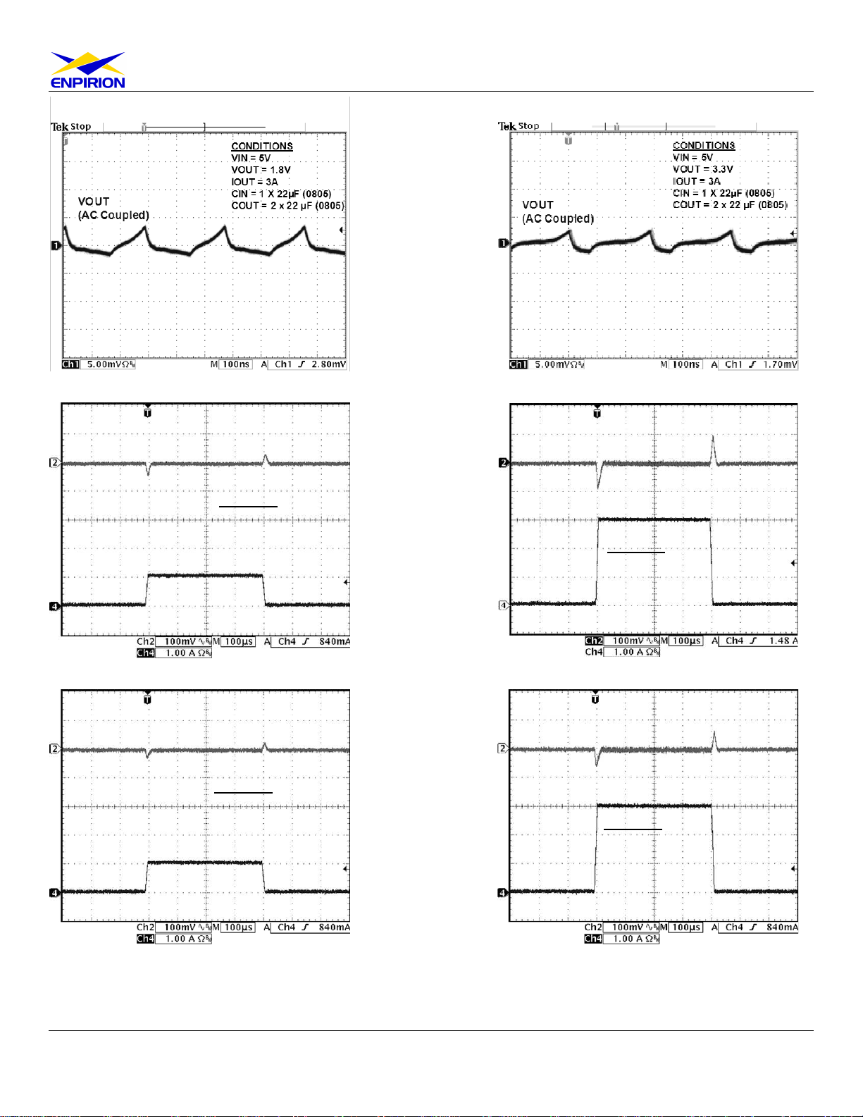
Output Ripple at 20MHz
VOUT
(ACCoupled)
Load Transient from 0 to 1A
CONDITIONS
VIN = 3.3V
VOUT = 1.8V
CIN = 1 X 22µF (0805)
COUT = 3 x 22µF (0805)
LOAD
VOUT
(ACCoupled)
Load Transient from 0 to 3A
CONDITIONS
VIN = 3.3V
VOUT = 1.8V
CIN = 1 X 22µF (0805)
COUT = 3 x 22µF (0805)
LOAD
VOUT
(ACCoupled)
Load Transient from 0 to 1A
CONDITIONS
VIN = 5V
VOUT = 2.5V
CIN = 1 X 22µF (0805)
COUT = 3 x 22µF (0805)
LOAD
VOUT
(ACCoupled)
Load Transient from 0 to 3A
CONDITIONS
VIN = 5V
VOUT = 2.5V
CIN = 1 X 22µF (0805)
COUT = 3 x 22µF (0805)
LOAD
Output Ripple at 20MHz
February 2012 R1.0
Page 7 of 8
Enpirion 2012 all rights reserved, E&OE www.enpirion.com
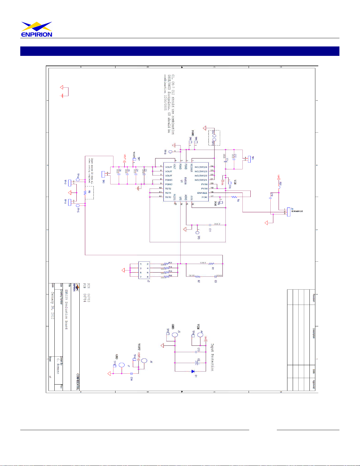
Evaluation Board Schematic
Figure 4. Engineering Evaluation board schematic.

February 2012 R1.0
Page 8 of 8
Enpirion 2012 all rights reserved, E&OE www.enpirion.com
Contact Information
Enpirion, Inc.
Perryville III
53 Frontage Road Suite 210
Hampton, NJ 08827
Phone: +1 908-894-6000
Fax: +1 908-894-6090
Enpirion reserves the right to make changes in circuit design and/or specifications at any time without notice.
Information furnished by Enpirion is believed to be accurate and reliable. Enpirion assumes no responsibility
for its use or for infringement of patents or other third party rights, which may result from its use. Enpirion
products are not authorized for use in nuclear control systems, as critical components in life support systems
or equipment used in hazardous environment without the express written authority from Enpirion.
Table of contents
Other Enpirion Motherboard manuals


