EUPA VXZA User manual

VXZA
Socket 370 ATX
Motherboard
USER’ S MANUAL
Model : VXZA
Manual Version :English, version 1.2
Release Date :July 28th , 2000

Copyright
Copyright 2000 by this company. All rights reserved.
No part of this publication may be reproduced, transmitted, transcribed,
stored in a retrieval system or translated into any language in any form or by
any means, electronic, mechanical, magnetic, optical, manual or otherwise,
without the prior written consent of the copyright holders.
User’s Notice
The contents of this publication are subject to change. This company
reserves the right to alter the contents of this publication at any time and
without notice.The contents of this publication may contain inaccuracies or
typographical errors and is supplied for informational use only.
Intel and Pentium are registered trademarks of Intel Corporation.
OS/2 and IBM are registered trademarks of Intemational Business Machines.
Windows and MS-DOS are registered trademarks of Microsoft Corporation.
AWARD is a registered trademark of Award Software Inc.
Other brand, corporate, and product names may or may not be registered
trademarks or copyright of their respective companies.

FCC & DOC Compliance
Federal communications Commission Statement
This device complies with FCC Rules Part 15. Operation is subject to the following two
conditions:
!This device may not cause harmful interference.
!This device must accept any interference received, including interference
that may cause undesired operation.
This equipment has been tested and found to comply with the limits for a Class B
digital device, pursuant to Part 15 of the FCC Rules. These limits are designed to
provide reasonable protection against harmful interference in a residential installation.
This equipment generatesm uses and can radiate radio frequency energy and, if not
installed and used in accordance with the manufacturer’s instructions, may cause harmful
interference to radio communication. However, there is no guarantee that interference
will not occur in a particular installation. If this equipment does cause harmful inter-
ference to radio or television reception, which can be determined by turning the equip-
ment off and on, the user is encouraged to try to correct the interference by one or more
of the following measures:
!Re-orient or relocate the receiving antenna.
!Increase the separation between the equipment and the receiver.
!Connect the equipment to an outlet on a circuit different from that to which
the receiver is connected.
!Consult the dealer or an experienced radio/TV technician for help.
Warning
The use of shielded cables for the connection of the monitor to the graphics card is re-
quired to assure compliance with FCC regulations changes or modifications to this a
uthority to operate this equipment.

Chapter 1 Overview
General Description.....................................................................................1-1
Check Your Items.......................................................................................... 1-1
VXZA Specifications.....................................................................................1-2
VXZA Components........................................................................................1-
Motherboard Layout................................................................1-5
Chapter 2 Hardware Installation
Set Jumpers...................................................................................................2-2
Install CPU................................................................................................2-
CPU Setting..................................................................................................2-4
Clear CMOS.................................................................................... 2-4
Jumperless setting............................................................................2-5
Jumper setting......................................................................................2-8
System Memory Installation...........................................................................2-9
Install DIMM.......................................................................................2-10
Removing a Memory Module...........................................................2-10
Install Expansion Cards..................................................................................2-11
Connector Devices........................................................................................2-12
Panel Connector.................................................................................2-12
Power Connector.................................................................................2-12
PS/2 Mouse & Keyboard Connectors................................................2-1
Fan Connector......................................................................................2-1
USB device Connector........................................................................2-14
Serial Device (com1, com2), VGA & Printer Connectors................2-14
Floppy drive Connector......................................................................2-15
IrDA Connector...................................................................................2-15
IDE Hard Drivers Connector..............................................................2-16
AMR & AC97 Connector...............................................................2-16
LAN & MODEM Wake Up Connectors...........................................2-17
Game/Audio & CD_IN Connectors...................................................2-17
Contents

Contents
Chapter 3 CMOS Setup Utility
CMOS Setup Main Menu............................................................................ -1
Standard CMOS Setup................................................................................... -
Advanced BIOS Features............................................................................... -5
Advanced Chipset Features............................................................................ -8
Integrated Peripherals..................................................................................... -14
Power Management........................................................................................ -18
PnP / PCI Configurations............................................................................... -24
PC Health Status........................................................................................... -26
Frequency / Voltage Control.......................................................................... -27
Load Fail-Safe Defaults................................................................................. -28
Load Optimized Defaults............................................................................... -28
Set Supervisor / User Password.................................................................... -29
Save & Exit Setup.......................................................................................... -28
Exit Without Saving....................................................................................... -28
Chapter 4 Software Utility
Installing Interface..........................................................................................4-1
Installing Drivers Location.............................................................................4-2
Installing ADOBE Acrobat Read Driver........................................................4-2

Check Your Items
This VXZA motherboard package contains the following items. Please inspect the package
contents and confirm that everything is there. If anything is missing or damaged, call your
vendor for instructions before operating.
The Package includes:
!One VXZA motherboard
!One Floppy Interface Cable
!One IDE Interface Cable
!One Motherboard Resource CD
!One User’s Manual
General Description
Thanks for purchasing VXZA Socket 370 motherboard.VXZA is based on VIA chipset
(North Bridge VT82C694X & South Bridge VT82C686A). Its new features include that it
support AGP 2x/4x, super I/O, and voltage, temperature, and fan speed hardware monitoring,
and there are four USB connectors on board as well. It includes all of the required specifica-
tions like Ultra DMA 66 interface, meanwhile it supports PC 133 system memory. VXZA
provides you perfect function to be the same with your system operation and end user. This
user’s manual contains all the information and features that show you how to use the VXZA
motherboard. Please take a moment to familiarize yourself with the design and organization
of this manual.
Chapter 1
Overview
1-1

VXZ A Specifications:
Overview
1-2
Form Factor • ATX form factor
Board Size •30.5cm x 19.7cm
CPU
• Supports Socket 70 Intel P!!! & Celeron (PPGA), Celeron (FC-PGA) and VIA
Cyrix III
• Supports CPU Clock Frequency: 66/100/1 MHz
System Memory • DIMM 168-pin x SDRAM maximum1.5G
• Supports 64M-bit SDRAM technology
Chipset
• VIA Chipset including:
- VIA VT82C694X (North bridge)
- VIA VT82C686A (South bridge)
Expansion Slots
• 1 x AGP Slot
• 5 x PCI Slots
• 1 x ISA Slot.
• 1 x AMR Slot
Serial Port • Two serial ports UART 16550 compatible
Parallel Port
• One parallel port supports:
- SPP-standard parallel port
- EPP-enhanced parallel port
- ECP-extended capabilities port
Floppy Interface
• Support drivers inches / format with
- .5 inches-720KB/1.44MB/2.88MB
- 5.25 inches- 60KB/1.2MB
IDE Interface • The VT82C686A includes dual channel master mode PCI support 4 IDE devices.
• Support PIO Mode 4, ULTRA DMA / & ULTRA DMA/66
USB Port • Four USB ports supported
• Support USB Legacy Keyboard function
PS/2 Mouse • PS/2 mouse supported by connector onboard
PS/2 keyboard • PS/2 keyboard supported by connector onboard
Sound Function • On-board AC'97 System
• VT1611A Audio Codec
Fuse • Supports Recoverable fuse for USB, KB & MOUSE
RTC and Battery • Built in South Bridge
• Lithium (CR-20 2) battery
Power Connector • AT X
Wake up Function
• Modem ring wake up
• LAN wake up
• RTC Alarm wake up
Hardware Monitor
• System fan speed monitor
• Voltage monitoring
• Over temperature monitoring
BIOS
• Award BIOS
• Supports Suspend TO RAM (optional)
• Supports APM, DMI and ACPI
• Supports virus warning
• Supports Flash / Upgrade BIOS functions
LED Indicator • System Power LED
• HDD activity LED
1-3
Overview
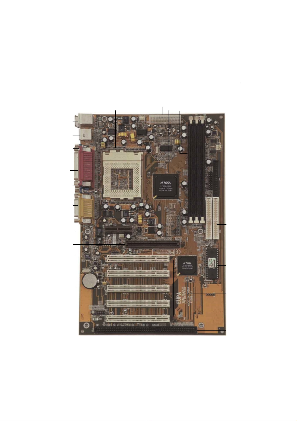
VXZA Components:VXZA Components:
VXZA Components:VXZA Components:
VXZA Components:
1234
5
6
8
7
9
10
11
12
13
14
14
15
16
17

Overview
1-4
Please refer to next two pages about each component, and this manual will
explain every important one at the following chapter.
1. Socket 370 processors socket
2. ATX Power Port
3. North Bridge VIA VT82C694X
4. DIMM sockets
5. Floppy Port
6. IDE Ports
7. BIOS
8. South Bridge VIA VT82C686A
9. Peripheral Component Interface (PCI) Slots
10. Industry Standard Architecture(ISA)
11. Accelerated Graphics Port (AGP) slot
12. Audio Modem Riser Card (AMR) slot
13. Audio Port --Mic in(pink), Line in(blue), Line out(green)
& Joystick Game Port
14. COM1 & COM2
15. Printer Port
16. USB devices ports
17. PS/2 Keyboard (purple) / Mouse (green)
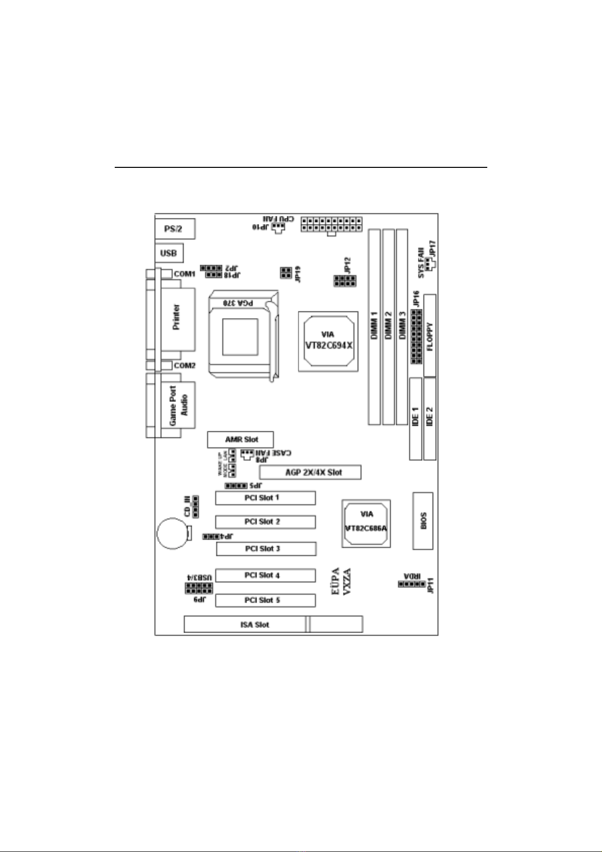
Motherboard Layout:Motherboard Layout:
Motherboard Layout:Motherboard Layout:
Motherboard Layout:
1-5
Overview

Jumpers
1. JP4 Clear CMOS
2. JP2, JP18 Select CPU’s type
3. JP12, JP19 CPU Clock Frequency
4. JP5 AMR & AC97 jumper setting
Expansion Slots
1. AGP AGP Expansion slot
2. PCI slot1 to slot5 32-bit PCI Bus Expansion slot
3. ISA slot 16-bit ISA Bus Expansion slot
4. AMR AMR Expansion Slot for AC’97 and MC’97
5. DIMM 1 to DIMM 3 Support 168-pin DIMM Memory
Connectors
1. IDE 1/ IDE 2 Primary IDE Connector / Secondary IDE Connector
2. Floppy Floppy Drive Connector
3. IrDA (JP11) Infrared Ray Port Connector
4. SYS Fan (JP17) System Fan Connector
5. CPU Fan (JP10) CPU Fan Connector
6. Chassis Fan (JP8) Chassis Fan Connector
7. Wake on LAN LAN Wake Up Connector
8. Wake on MODEM MODEM Wake Up Connector
9. ATX Power ATX Power Connector
10. COM1/COM2 Serial Port1/Serial Port2 Connector
11. CD_IN (JP1) Audio CD-IN Connector
12. Audio/Game Port Audio / Game Port Connector
13. Printer Printer (Parallel) Port Connector
14. USB Universal Serial Bus Port1 and Port2
15. PS/2 connectors PS/2 Mouse & PS/2 Keyboard Connectors
16. JP9 USB Connector 3/4
17. Panel
-PowerOn ATX Power on / off switch (2-pin)
-Reset Reset Switch Connector (2-pin)
-HDD LED HDD LED Connector (3-pin)
-Power LED ATX Power LED Connector (3-pin)
-Speaker Chassis Speaker Connector (4-pin)
-KBLCK Keyboard Lock Switch Connector(2-pin)
Overview
1-6

Chapter 2
Hardware Installation
This chapter gives you a step-by-step procedure on how to install your system and
set jumper. The motherboard has several user-adjustable jumpers on the board that
allow you to configure your system to suit your requirements.
Cautions: Protecting Against Electrostatic Discharge
Static electricity can harm delicate components inside your system. To prevent static
damage, discharge static electricity from your body before you touch any of your
motherboard electronic components,such as the microprocessor.Observe the follow-
ing precautions:
- Do not removes the motherboard from its anti-static packaging until you
are ready to install it into a computer case.
- Before you handle the motherboard in any way, touch a grounded, antistatic
surface, such as an unpainted portion of the system chassis, for a few
seconds to discharge any built-up static electricity.
- Handle add-in cards and modules by the edges or mounting bracket.
2-1

Set Jumpers:
umpers are used to select the operation modes for your system. Some jumpers on
the board have three metal pins with each pin representing a different function.A
1 is written besides pin 1 on jumpers with three pins. To set a jumper, a black
cap containing metal contacts is placed over the jumper pin/s according to the
required configuration. A jumper is said to be shorted when the black cap has been
placed on one or two of its pins. The types of jumpers used in this manual are
shown below:
Note:
Users are not encouraged to change the jumper settings not listed in this manual.
Changing the jumper settings improperly may adversely affect system performance.
Open Short
Jumper Cap 2-pin Jumper 3-pin Jumper Jumper Block
1
2
31
2
3
Hardware Installation
2-2
Hardware Installation
2-3
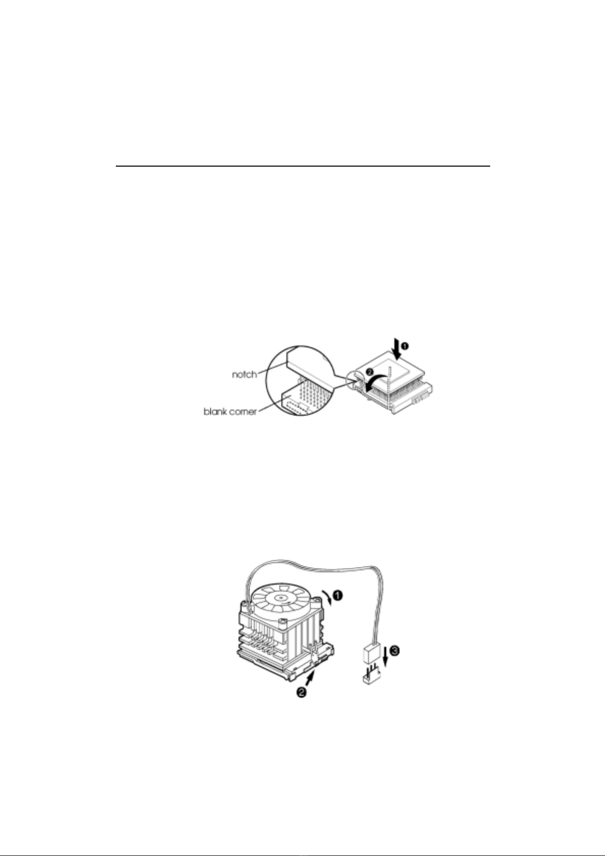
Install CPU
The CPU module resides in the socket 370 on the motherboard.Please following the
steps introduced below to complete the CPU installation.
1) Locate the new processor you are installing over the socket so that the notched
corner on the processor (pin 1) can be aligned with the blank corner on the
socket. Then gently push the processor straight into the socket until its pins
are completely inserted into the holes of the socket.
Caution:
If you install the processor chip in the wrong orientation, you may burn the chip
and void your warranty. So you should install it careful deeply.
2) Press the ZIF handle back to close it.
3) Attach the heat sink to the processor socket and then connect a fan connector
cable from the CPU fan to the CPU fan connector.

Hardware Installation
2-4
CPU SettingCPU Setting
CPU SettingCPU Setting
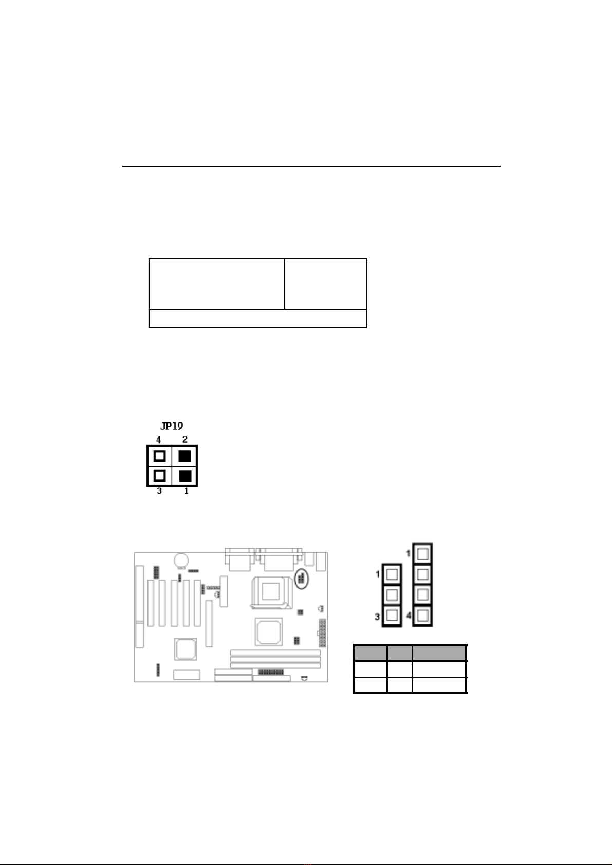
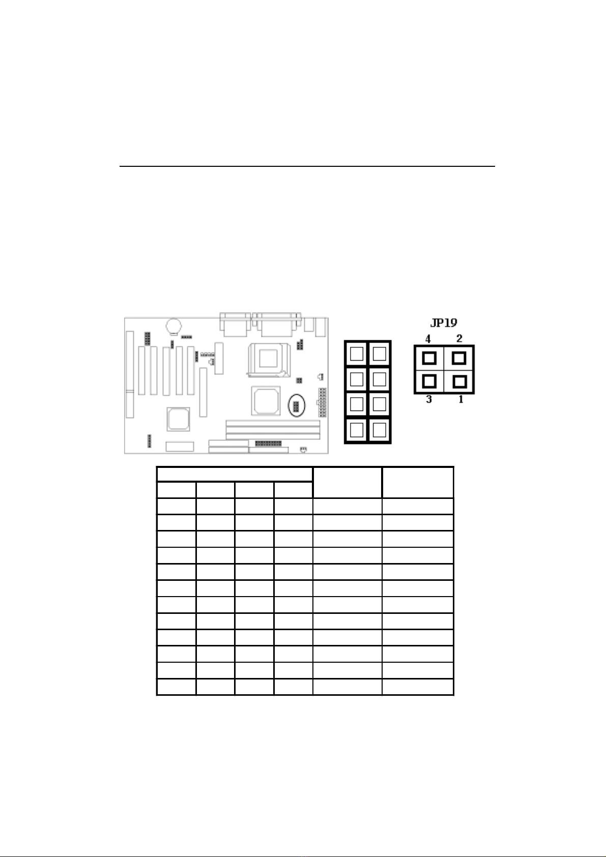
CPU Setting (jumperless & jumper setting)
After installing the CPU, you must set the clock selection jumpers to match the
frequency of the CPU. There are two ways for CPU setting: jumper setting and
jumperless. Find the jumpers labeled JP12, JP19, set these jumpers according to
the figure below and table for CPU Clock Frequency.
Caution: we dont recommend user to try overclock, it may damage your
CPU and result in a slower speed. Please think carefully before
you use overclock function.
We introduce you how to clear CMOS, and enter into system BIOS, it could help you
accomplish CPU setting in BIOS easyly.
Clear CMOS:Clear CMOS:
Clear CMOS:Clear CMOS:
Clear CMOS: JP4
JP4 CMOS
To Clear CMOS, please follow the steps below:
1. Power off the system and unplug the chassis AC power cord.
2. Short JP4 at pin 2-3 for few seconds.
3. Set JP4 back to its Normal position at pin1-2
4. Plug the AC power cord to the chassis.
5. Power on the system and load the BIOS set up default.
Clear
CMOS
Default
(Normal)

Hardware Installation
2-5
Jumperless setting: JP19
Caution:
JP12 must be open when adjusting CPU setting by jumperless(JP19).
Auto Detect
Meanwhile, the jumperless mode allow processor settings to be made through the
BIOS setting. (Frequency / Voltage Control)
How to enter the BIOS?
While the BIOS is in control, the Setup program can be activated by pressing the
<Del>key during the POST (Power On Self-Test).
2-Pin Jumper
SHORT
OPEN
Auto Detect is default for CPU of P19. You need not
set this jumper except you want to over-clock.
We recommend you to keep the default, it will guaran-
tee your system working stability.

Hardware Installation
2-6
CPU Host Clock (CPU/PCI)
Default....................( )
100/33 MHz..............( )
103/34MHz.................( )
112/37MHz.................( )
124/41MHz...................( )
Frequency / Voltage Control
Auto Detect DIMM / PCI Clk
Spread Spectrum.
CPU Host Clock (CPU / PCI)
Enabled
Disabled
De ault
Item Help
Menu Level !
Enter: Select F5 : Previous Values +/-/PU/PD: Value F10: Save
F6 : Fail-sa e de aults Esc:Exit F1: General Help F7 : Optimized De aults
CPU Host Clock (CPU/PCI)
Default....................( )
66/33 MHz..............( )
75/37.5MHz.................( )
83/41.7MHz.................( )
2. If your CPU is 100MH clock frequency (FC-PGA Coppermine & VIA
CyrixIII), you may select CPU host clock from the BIOS for over-clock.
1. If your CPU is 66MHz clock frequency (Celeron), you may select CPU
host clock from the BIOS for overclock.
Auto Detect DIMM / PCI Clk
Spread Spectrum.
CPU Host Clock (CPU / PCI)
Enabled
Disabled
De ault
Item Help
Menu Level !
Enter: Select F5 : Previous Values +/-/PU/PD: Value F10: Save
F6 : Fail-sa e de aults Esc:Exit F1: General Help F7 : Optimized De aults
If you decide to make 66MHz CPU over-clock to 100MHz CPU, you may set
JP19 pin 3-4 short as following:
Frequency / Voltage Control
Caution!!
Frequencies above 100MHz exceed the specifications
for the CPU and are not guaranteed to be stable and
results in damanging your peripheral devices.
Hardware Installation
A uto Detect DIM M / PCI Clk
Spread Spectrum.
CPU Host Clock (CPU / PCI)
Enabled
Disabled
De ault
Item Hel p
Menu Level !
Enter: Select F5 : Previous Values +/-/PU/PD: Value F10: Save
F6 : Fail-sa e de aults Esc:Exit F1: General Help F7 : Optimized De aults
CPU Host Clock (CPU/PCI)
Default....................( )
133/33 MHz..............( )
140/35MHz.................( )
150/37MHz.........................( )
Caution!!
Frequencies above133MHz exceed the specifications
for the CPU and are not guaranteed to be stable and
results in damanging your peripheral devices.
Frequency / Voltage Control
3. If your CPU is 133MHz clock frequency (FC-PGA Coppermine & CyrixIII),
you may select CPU host clock from the BIOS for over-clock.
If you decide to make 66MHz CPU or 100MHz CPU to 133MHz CPU or high, you
may set JP19 pin1-2 short as following:
2-7
CPUType Selection: JP18,JP2
JP18
JP2
JP2 JP18 CPU TYPE
2-3 1-2 Intel, CyrixIII
1-2, 3-4 2-3 Joshua
Hardware Installation
Jumper setting: JP12
You can set P12 to adjust the frequency manually according to the figure below
and table which is fit for you most.
Note: Jumperless mode(JP19) must be opened when adjusting CPU
setting manuall .
JP12
JP12 CPU Freq
(MHz) PCI Freq (MHz)
7-8 5-6 3-4 1-2
Open Open Open Open 133.3 33.3 (CPU/4)
Open Open Open Short 124 31 (CPU/4)
Open Open Short Open 150 37.5CPU/4)
Open Open Short Short 140 35 (CPU/4)
Short Open Open Open 100 33.3 (CPU/3)
Short Open Open Short 133.3 44.43 (CPU/3)
Short Open Short Open 112 37.3 (CPU/3)
Short Open Short Short 103 34.3 (CPU/3)
Short Short Open Open 66.8 33.4(CPU/2)
Short Short Open Short 83.3 41.7 (CPU/2)
Short Short Short Open 75 37.5 (CPU/2)
Short Short Short Short 124 41.3 (CPU/3)
open
2-8
Hardware Installation
2-9
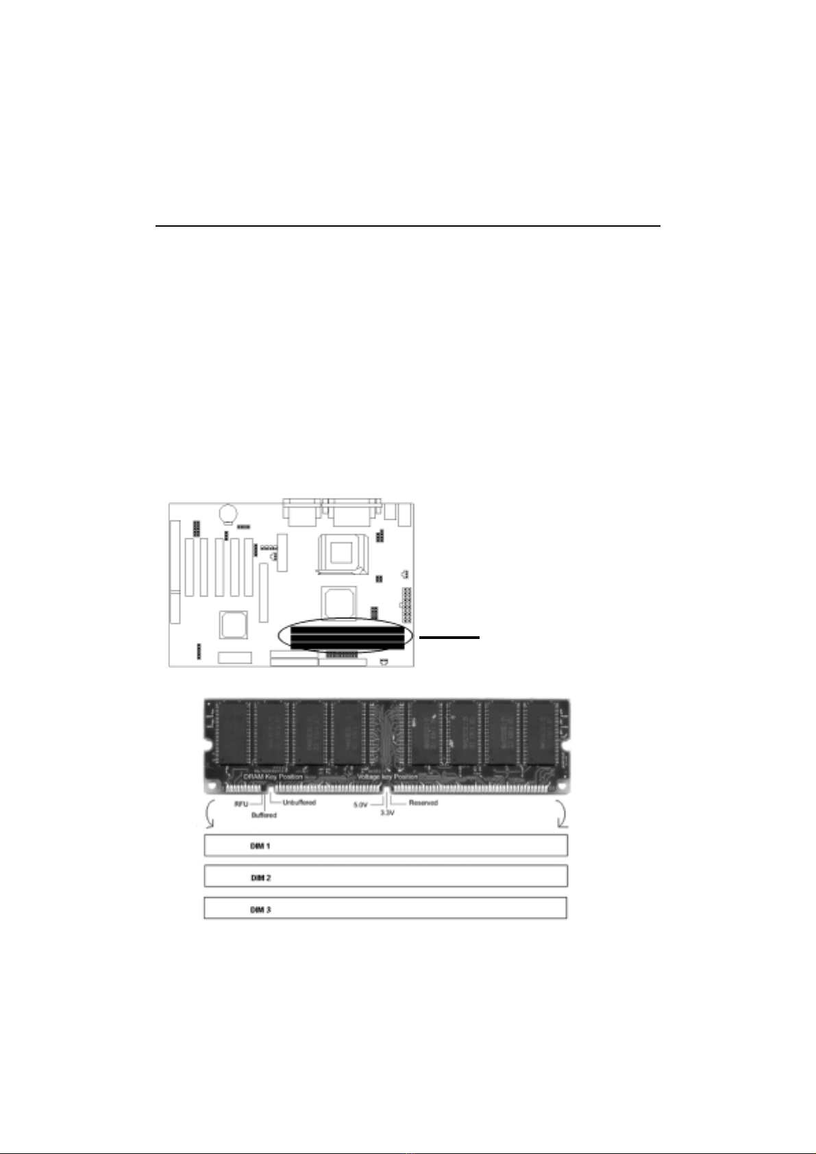
System Memory InstallationSystem Memory Installation
System Memory InstallationSystem Memory Installation
System Memory Installation
There are 3 pieces 168-pin DIMM (Dual Inline Memory Module) sockets on the
motherboard which support SDRAM and EDO DRAM memory.
♦To ensure reliability, it is recommended to use PC 100 SDRAM or PC 133 SDRAM
for your high cloc SDRAM performance requirement.
♦If you are using low cloc SDRAMs, you should set the SDRAM cloc option of
the BIOSs Chipset Feature Setup to HCLK-33 to ensure stability.
♦DIMM Sizes supported: 8MB, 16MB, 32MB, 64MB, 128MB, 256MB.
♦Total Memory Size = DIMM1 + DIMM2 + DIMM3, maximum up to 1.5GB.
There are 3x168-pin DIMM
slots (DIMM1, DIMM2, DIMM3)
that allow you to install the system
memory max up to 1.8 B SDRAM.
Other EUPA Motherboard manuals


