connection between different sections.
connection within same section.
Arrows indicate direction of signal or energy flow.
♦The symbol without an additional label denotes Vcc (+5V).
♦Capacitance in microfarads unless otherwise indicated.
♦These drawings based on unit with Serial No. 302.500.
Log
♦1996 Jul: Initial drawing / bhilpert.
♦2004 Oct: CMU & manual control notes added. N4 and N5 renamed to NK and NR.
♦2017 May: Format updates.
♦2020 Oct: Substituted 5962 ICs redrawn as 5330s to be consistent with PCB design.
Prefix of IC names changed from “IC” to “U”.
Separator for IC pin names changed from “-” to “.”.
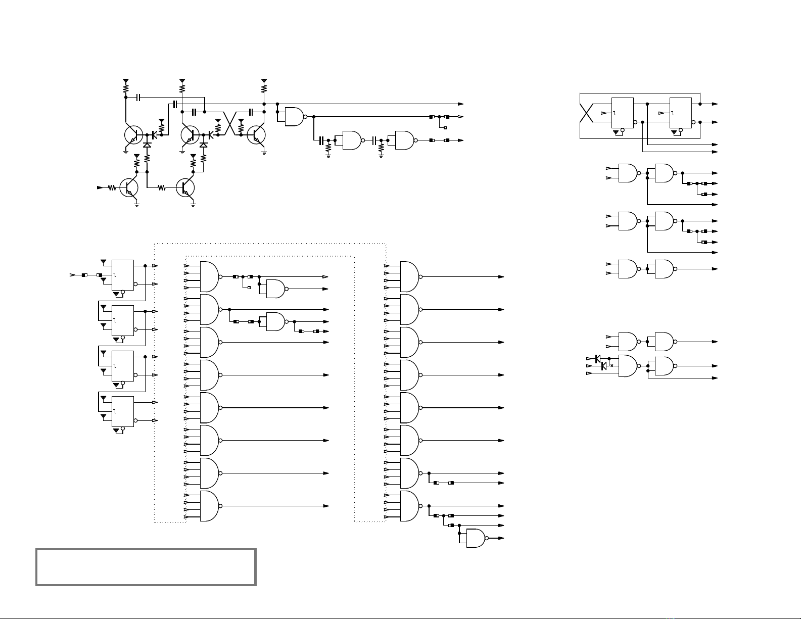
OP-Cycles and Manual Control of Operations
A switch can be plugged into the remote connector (NR) to provide the ability to single-step through the major state cycles of an
operation. See the Keyboard & OP page for wiring of the switch.
An OP-cycle is a full number cycle during which processing occurs and is indicated by the OP signal. Major state transitions
occur at the end of an OP-cycle. Simple user operations such as numeral entry generate a single OP-cycle without sending P0 to
0. More complex operations requiring multiple number cycles generate a first OP-cycle and send P0 to 0. Multiple OP-cycles are
subsequently generated until the operation is complete, at which time P0 returns to 1.
Enabling the MANUAL switch disables the automatic generation of OP-cycles for multi-cycle operations. In this mode, once a
multi-cycle operation has been initiated, each press of the CLE key generates a single OP-cycle, so the operation can be stepped
through one OP-cycle at a time.
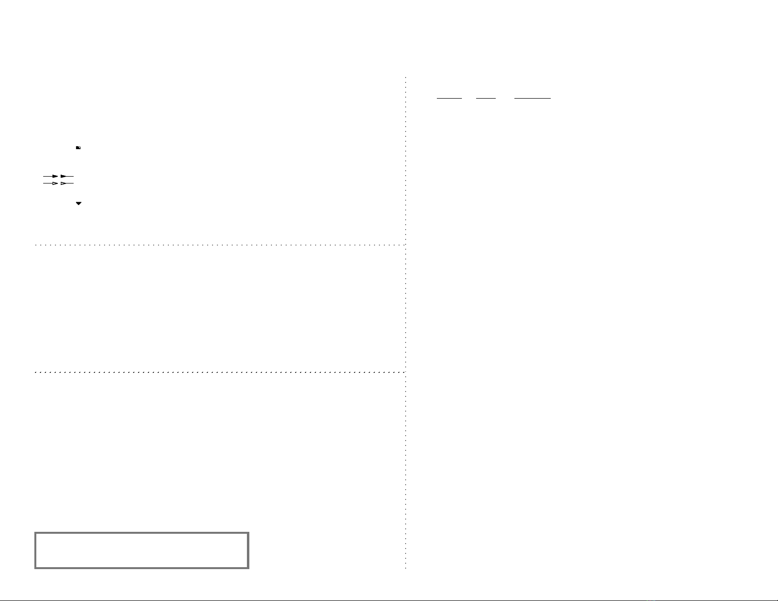
Signal Names
Section Signal Description
Timing Ø… Master timing.
ØMaster clock from which all timing is derived. This is the basic bit rate.
ØB… Bit timing.
ØD0…ØD15 Digit Timing. 16 digit intervals, ØD2–ØD15 are the displayed digit time periods;
Registers do not cycle during ØD0.
Keyboard K
…
various (unlatched) indications from the keyboard.
A1=Add, 0=subtract.
C1=calculation is multiply or divide, 0=add or subtract.
M1=Multiply
D1=Divide
N1=Normal mode, 0=use the Z register, also associated with the decimal point.
OP OP… Operation cycle.
Control P0 state 0 of the 2-bit P state register: 1=idle, 0=calculating.
P1 – P3 the other 3 states of the P register indicating some aspect of calculation.
R0 – R3 the 4 states of the 2-bit R state register.
S
<p><r>
shorthand for states of the P and R register: S
<p><r>
= P
<p>
• R
<r>
.
DISP 1=displaying, 0=calculating , same as P0 but with additional control from
connector N5.
CY… Outputs from control to the Y register.
CX… “the X register.
CZ… “the Z register.
CA… “select the source for the A input of arithmetic.
CB… “select the source for the B input of arithmetic.
CS… “select the arithmetic function.
CD… “the decimal point register.
CQ… “ the Q flag.
X Register X… The operand being displayed.
X1,X2,X4,X8 BCD numerals on their way to the display.
Y Register Y… The second operand.
Y
YP1
Z Register ZThe user memory.
DP Register DP… The decimal point register.
Arithmetic ASUM16 The raw digit sum from the serial adder, base 16.
ASUM10 The normalized digit sum after correcting for values between 10 and 15 inclusive.
Q Flag QThe 1-bit Q flag for catching data conditions.
Display Latch DL… Latch for numerals during the digit display interval, also used for transferring from
the DP register to the Y register.
♦A lowercase “n” in a symbol name indicates the logical NOT operation.
♦The character “ • ” in a symbol name indicates the logical AND operation.
♦The character “+” in a symbol name indicates the logical OR operation.
Algorithm Notes
♦During multiply and divide, a hex ‘F’is placed after the LSD of one of the operands. The operand is shifted up to
the upper end of the register and the F is used to indicate where arithmetic will begin during the number cycle.
♦During multiply and divide, the uppermost digit of the Y register is used as a digit counter to limit the multiply/divide
loop.