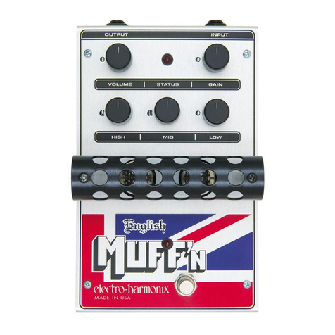
PRINCETON RECORDING AMP®™
(This is the model name for warranty claims)
6
resistor is R10. The amplified signal from V-4-B
couples to the simple “concertina” phase inverter cir-
cuit (V4-A). Note the 56kOhm in the cathode and
plate circuit. Both outputs are close, but not perfect
180 degree matches of each other. The bias of the
phase inverter is intentionally non-ideal as per the
vintage Princeton Reverb. Single sided clipping can
be observed on the waveform when driven hard.
This clipping causes the output power to not reach
the full capability that the 6V6s can provide.
Each output phase is separately ac-coupled to the
6V6 output tubes (V5 & V6). The Green & Blue
leads of the output transformer are connected to the
6V6’s plates with B+ voltage applied to the RED cen-
ter tap (approximately +400V). The nominal
impedance of the OT’s secondary is 8 ohms.
The 6V6’s negative bias is set by an adjustable bias
circuit found on the TZ/FX PCB. Its typical voltage
drive is -36.7 VDC. This voltage is set by measuring
the voltage across R20 (1 ohm) on the Main Tube
PCB. The specified dc voltage across R20 is 40mV,
which ideally relates to 40mA or 20mA per 6V6.
The heaters for 2 tubes (V1 & V3) are powered by a
dc filament drive (using +/-16V from the TZ/FX PCB).
AC filament drive is utilized on the remainder of the
tubes and is derived from the green secondary of the
PT. R1 & R3 act as a hum balance circuit for the AC
filament drive. The pilot lamp is not energized by the
AC filament supply.
TUBE POWER SUPPLY
The Tube PCB’s Primary PCB subassembly inter-
faces between the AC line inlet, the AC power
switch, and the primary of the power transformer. It
provides inrush limiting with RT1 and line filtering
with C19.
The red secondary of the PT energizes the Tube
PCB’s Power Supply PCB subassembly. D4-7 is a
bridge rectifier and directly feeds the B+ filter cap
(C26). The screen grid supply (A) follows, coupling
through a 1k resistor. Supplies C & D are developed
by subsequent RC filter sections. The C supply
feeds the phase inverter & the D supply energizes
the previous preamp stages.
TZ/FX/IO PCB
Only certain components found on this PCB are field
serviceable. Please refer to this documents’ parts
list to determine its serviceability status.
The TZ/FX/IO PCB is composed of 2 PCB subas-
semblies. The TZ/FX PCB subassembly contains
the following circuitry: the compressor circuit, the
overdrive circuit, the solid-state power supplies, the
Trans-Impedance (TZ) amp, the silent adapter cir-
cuit, the TZ mode selector, and miscellaneous
control circuitry. On the IO PCB subassembly, one
finds the footswitch interface with its supporting con-
trol circuitry, the external effect loop, the headphone
interface, and the line out interface.
IO PCB
On the IO PCB subassembly, one finds the foot-
switch interface with its support circuitry, the external
effect loop, the headphone interface, and the line out
interface. This subassembly is found in its entirety
on page 4 of 0069346000. Much of this subassem-
bly is field serviceable.
The Main Tube PCB sends the IO PCB a reduced
signal output, one which is suitable for the solid-state
effects loop found there. The signal enters the EF-
FECTS LOOP SEND signal chain via coax at WJ34
(referenced to WJ31). U6 – A & B are a high input
impedance differential buffer and amplifier which in-
crease the output level at the effects loop jacks to a
nominal -10dBu. At the output of U6-B, the signal
takes 2 paths. The path to R72 wraps around the
effects loop jacks in order to bypass it when config-
ured in the EFFECTS LOOP KILL state. The other
path is taken if the effects loop is functional. When
Q3 is biased on, U2-B acts as a signal kill switch that
silences J3 when the loop is killed. When Q3 is bi-
ased off, U2 - B is a simple inverter. Resistors and
capacitors build out the U2-B’s output to J3 providing
protection & EMI filtering.
J2 is the external effects return jack. Its signal
source is switched depending on whether a plug is
installed in it (no plug = pass-thru). U2-A is a differ-
ential buffer acting as the FX return receiver. U7-A is
1) an attenuator to compensate for U6-B’s boost and
2) the signal selector for the foot-switchable external
effects on/off function. This is followed by a differen-

