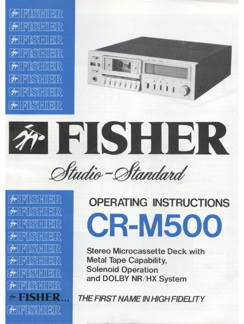
Fisher PH 415K User manual

•
•
•
~---.YII
-----J
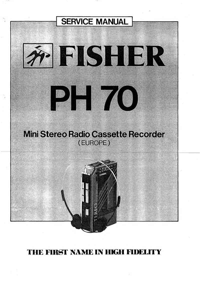
SERVICE MANUAL
1-----------=,--------
~FISHER
PH4
PORTABLE HIGH FIDELITY STEREO
RADIO/CASSETTE RECORDER
The
first
name in high
fidelity
us

SPECIFICATIONS-----------------------
Power Source
AC .............................
DC
............................
Output Power ............
Power Consumption..
Recording System ....
Erasing System
..
..
.
Tape Speed .........
Fast Forward Time
RewidTime
...
Wow & Flutter ................
Frequency Response
...
.
.....AC120/210/240V, 60Hz
.12V(UM-1. D Cell. HP2,
A20, Monozellen x
8)
.......4.0 W X 2 (10%)
.......
25W
.....
AC
Bias
...........
AC
Erasing
........4.75 cm/sec.
±3%
.110sec.(C-60 cassette)
.
11
0sec.(C-60 cassette)
.0.06 % WRMS
.......60 -12500Hz
Signal to noise Ratio...............DOLBY NA
ON
Betterthan 60 dB
DOLBY NA OFF Better than
50
dB
Hum & Noise ...............................Less than
45
dBs
Crosstalk......
..
.............Better than 55 dB
Channel Separation ...............Better than 50 dB
Terminal Impedance
MIC
..
Ext. Speaker
Headphone .........
Frequency Range
MW......
........
...
3.3 k ohms
.......8 ohms
..8 ohms
......530 -1.605 kHz
............2.3 -7.0 MHz
SW,
SW, .
FM
... ................... .7.0 -22.0 MHz
............................88 -108 MHz
ALIGNMENT
PROCEDURES:----------------------
FM ALIGNMENT Standard
test
frequency 400 Hz and deviation
22.5
kHz
Connections Frequency
Tunmg
Dial
Adiustment
Remarks
Step
Alignment
of Signal
INPUT OUTPUT
Generator
Setting
Calibration Place ouptut of Connect
input
/\
gene-scope
on
terminal
of
gene-
Turn
1
of
Trap
COll(L3)
scope to 10.7 MHz
Lowest
end
T1,T2
AMY
IF
TP1
TP2
marker
2 Cahbration
Connect
signal
Connect
VTVM
with 87.45 MHz
L4
Obtain
sme-curve
of
generator
to
antenna
4 ohm dummy load
and
maximum amplitude.
L--
Tuning Range terminal
(J
1)
and
oscilloscope
to
3 through dummy
speaker
108.25 MHz Highest end CT2
(PVC)
·t@
4 Adjustment antenna. terminal. 90 MHz 90 MHz
L1
-of
5 Tracking 106 MHz 106 MHz
CT1
(PVC)
6 Repeat the above adJustments
Use
a screwdriver
Wtlh
plastic grip for all
adJustment
MW ALIGNMENT Standard test frequency 400 Hz and
modulation
30% at AM
Connections
Frequency Tuning Dial
Step Alignment INPUT OUTPUT of Signal Setting Adjustment Remarks
Generator
Calibration
Connect
standard
Obtain
symmetncal
curve
1 of IF loop antenna to Connect
VTVM
with
and
maximum amplitude.
for AM
output
terminal
cf
4 ohm dummy load
M1x(l:\'\
Adjustment gene-scope.
and
oscilloscope
to
455 kHz Lowest
T3
and
T4
2 of Place bar antenna
Ext
speaker end
IF Gain 60
cm
away
from terminal
~
loop
antenna z
3 Calibration Connect standard 515 kHz L10 Obtain sine·wave of 400
Hz
L---
ot
loop
antenna
to
Connect
VTVM
with
and
maximum amplitude
4 Tuning Range output of signal 4 ohm dummy load 1620 kHz Highest end CT3
~~
generator.
and
oscilloscope
10
5 Ad1ustment Place bar antenna Ext. speaker 600 kHz 600 kHz
L7
~
ot 60
cm
away from terminal.
(MW
bar ant
COIi)
6 Trackmg
loop
antenna 1400 kHz 1400 kHz
en
7 Repeat the above ad1ustments
-1-
•
•
•
ALIGNMENT
PROCEDURES---------------------
sw1
ALIGNMENT
Connections
Frequency
Tuning
Dial
Step Alignment of Signal
INPUT OUTPUT Generator Setting
1 Calibratlon
of
Connect
signal
Tuning Range 2.25 MHz
Lowest
end
-
generator
to
Connect VTVM with
2 terminal (J1) 4 ohm
dummy
load 7.2 kHz Highest end
lhrough
dummy
and
oscilloscope
to
3
Adjustment
antenna.
Ext
speaker 2.5 MHz 2.5 MHz
-of
terminal.
4
Tracking
5 Repeat the above
adjustments
.
SW2 ALIGNMENT
Connections
Frequency Tuning Dial
Step Alignment INPUT OUTPUT
of
Signal Setting
Generator
1 Calibration
Connect
signal
Connect VTVM with 6.8 MHz Lowest end
-
of
generator
to
4 ohm dummy toad
2 Tuning Range
antenna
terminal
and
oscilloscope
to
23
MHz Highest
3 Adjustment through
dummy
f---
of
antenna
.
4 Tracking
5 Repeal the above adJustments.
FM MPX ALIGNMENT
Ext. speaker 7 MHz 7 MHz
terminal.
SWdummy
IT:-
Jt
antenna OQ
---:;;.,,
Connections
Adjustmenl
Remarks
Obtain sine-wave of 400Hz
L9
and
maximum
amplitude.
CT4
ME@)
L6
AdJustment
Remarks
L8
Obtain sine-wave of 400 Hz
and
maximum
amplitude.
CT8
·E@J
LS
Tuning
Dial
Step Alignment INPUT OUTPUT Setting Adjustment
Remarks
FM Connect TP2
Connect
Frequency
1 stereo to the GND. counter
to
TP3
-
SVR1
Obtain 19 kHz on the frequency
12
PIN
(IC2):
counter
.
CASSETTE AMP ALIGNMENT
No
Alignment Setting
Instrument
Connection
AdJusted
component Ad1ustment
1 Playback NORMAL, VTVM, test TP402-GND SVR401 580mV
level
Playback tape MTT150, (TP502-GND) (SVR501)
2 osc NORMAL, BEAT frequency R422 L404
60kHz±0
.tkHz
lrequency
CUT (1)
counter,
3
Bias
level
NORMAL, VTVM TP401·GND SVR403
4mV±0.1mV
CUT(t)
(TP501 •GND) (SVR503)
4 Repeat steps 2 and
3.
NORMAL, TP401•GND SVR402
5 Record level VTVM (TP50t-GND) 550,,V
Record
mode,
at
osc Stop (SVR502)
Note) ) right channel
-2-

ALIGNMENT
PROCEDURES---------------------
INSTRUMENTS TAPE SPEED ADJUSTMENT
Audio Signal generator two VTVM's, Frequency Counter, and Test
Tape
MTT
-1
14,
MTT-11
,.
MTT-150 or TDK
AD
PRILIMINRY
Load test tape
MTT-111
which has been recorded with a 3,000
Hz
test signal
2.
Place the FUNCTION
SELECT
switch
1n
the
TAPE
pos1t1on
•
remove
the
cabmet
to
access
the
need
and
other
adjusting
parts
3 Connect the frequency counter
to
the
LEFT
EXT
SP
Jack
in
parallel with the
VTVM
HEAD AZIMUTH ADJUSTMENT
1 Press
STOP/EJECT
Bullon to open
the
casselle case
2 Grasp the sides
of
the casselle case
hd
and pull
it
up to remove
the lid
3.
Load test tape MTT-114
in
the casselle case and close
11
4 Place the FUNCTION
SELECT
switch
1n
the
TAPE
position
5 Connect a
VTVM
to the
LEFT
EXT
SP
Jack,
and another
VTVM
to
the RIGHT
EXT
SP
Jack
VTVM
(MAX)
~L
·e·
,,
...
o~
__
,,.,o
Frequency counter
3kHz ± 60Hz
L
4 ohm
(2W)
Dummy load
4 Place the tape deck
1n
the play mode.
SPEAKERS
b~,,JL
'MIN4Q
V[lTVM
(MAX)
f
SPEAKERS
e 4 ohm (2W) '
'MIN
4Q
Dummy Load L
6 Place the tape deck
1n
the play mode
5.
Remove the label
on
the back of the motor and
adJuSI
the tnm
pot
1n
the motor for 2,940
Hz
to 3,060
Hz
reading on the fre-
quency
counter
Cover
the
adjustment
opening
with
a
piece
of
adhesive tape after the ad1ustment
1s
completed
AdJust
the head azimuth adJusting screw for maximum playback
output
on
the VTWM's
MECHANICAL ADJUSTMENT
Can
not
be
done.
ITEM
MODE
Pinch
roller
adjustment Playback
Take-up torque
adjustment Playback
Fast-forward and F.F
rew1nd1ng
torque
or
adJustment
rewind
Wow and fluller
JIS weighted Playback
SPEC
MEASUREMENT METHOD
Hook the spring gauge to pinch roller metal and pull
11
away
300"v500 from the capstan
gr
Measure
the
pressure
the
moment
the
pinch
roller
comes
1n
contact with
the
capstan
and
the
pinch
roller
starts
rotatmg
4Q"v70
Mount
the
cassette
torque
meter
in
the
same
way
as
the
casselle tape.
gem
The take-up torque
1s
shown
on
the torque meter
Mount
the
cassette
torque
meter
m
the
same
way
as
the
55"v150 casselle tape
g.cm
The
F.Forward
and
rewind
torque
1s
showh
on
the
torque
meter.
0.1%
Play back 3kHz (lset) tape and read with the wow meter
Pinch
roller
Fig-1
-3-
REMARKS
See
figure
1
-
-
-
•
•

•
•
•
PARTS
LIST(CASSETTE
MECHANISM\..-------------------
Key
No.
1
2R
2L
3
4
5
6
7
8
9
10
11
12
13
14
15
16
18
19
20
21
22
23
25
26
27
28
29
30
31
32
33
34
35
36
37
38
39
40
41
42
43
44
45
46
47
48
49
50
51
52
53
54
55
56
57
58
60
61
62
63
65
69
70
PART No. DESCRIPTION
O'ty
CASSETTE MECHANISM (R-S97106)
ATN-1715
01
501
ATN-1715
01
08
ATN-1715
01
07
ATN-1715
01
09
ATN-1710
01
10
ATN-1715 02
501
ATN-1715 02
02
ATN-1715 02
12
ATN·1710 02
01
ATN-1715 02 04
ATN-1715 02
13
ATN-1559 03
06
ATN-1710 03
501
ATN-1710 03 06
ATN-1710 03
301
ATN-1710 03 302
ATN-1710
03
16
ATN-1710 03 22
ATN-1710
03
18
ATN- 940 03 12
ATN-1710
03
19
R-S07411
R-S07412
ATN-1710 04
301
ATN-1715 09
301
ATN-1715
09
302
ATN-1715
09
03
ATN-1715 10
301
ATN-1715 05 302
ATN-1710 05 02
ATN-1710 05
06
ATN-1710 05 04
ATN-1710 05
09
ATN-1520 13 04
ATN-1200 12
01
ATN-1240 09
058
ATN-1710 06 03
ATN-1715 06 303
ATN-1715 23 06
ATN-1715 23 05
ATN-1710
11
03
ATN-1715 20 510
ATN-1715 20 503
ATN-1715
20
02
ATN-1715 20
05
ATN-1222 17 02
ATN-1715 20 06
ATN-1700
09
35
ATN-1715 20
14
ATN-1715 20 23
ATN-1715 20 24
ATN-1715 20
11
ATN-1715 20 13
ATN-1715 20 15
ATN-1510 09 28
ATN-1715 20 509
ATN•1715 20 25
ATN-1710
17
301
ATN-1710 17 302
ATN-1715 17
01
ATN-1715 22
501
ATN-1715
06
02
ATN-6401
01
36
ATN·6401
01
38
Chassis assembly
Cassetle holder R
Cassette holder L
Guide p,n
Guide
pm
cushion
REC
play
arm
assembly
Sensing
piece
Sensing
piece
spring
REC
safety lever
REC
safety lever spring
REC
slide lever
REC
slide lever spring
Head panel assembly
Pressuer
spring
Take up idler assembly
Take up idler shaft assembly
Take up roller shaft spring
Panel
press
plate
Head base
Head
spring
Collar
Record/Play head
Erase head
Pinch roller assembly
Take up reel assembly
Supply reel assembly
Back tention spring
RF
clutch assembly
Flywheel capstan assembly
Flywheel metal
Flywheel melal plate
Flywheel guide
Damper
spring
Motor
rubber
cushion
Collar
screw,
Motor
Main belt
Drive belt
Motor assembly
Eject stopper
Ejecl stopper spring
Coller
Push button lever
Push button flame
Push button base
Push
button
lever
spring
Pause
lever
Pause
lever
spring
Pause
stopper
Function
lever
spring
Function
lever
spring.
Switch plale
REC
stopper
RF
stopper
Plate stopper
REC
stopper spring
PAUSE button lever
Button
function
lever
Breake
arm
L assembly
Breake arm A
assembly
Breake spring
Switch
lever
Motor pulley
1
1
3
3
Switch 1
Swilch 2
Key
No.
72
73
74
75
76
77
78
79
80
81
82
83
84
85
86
87
88
89
90
91
92
93
94
95
96
97
98
99
100
101
102
103
104
105
106
107
108
112
302
303
304
305
306
308
309
311
312
310
314
315
316
317
318
319
320
321
322
323
325
326
327
328
329
324
PART No. DESCRIPTION
ATN·1715 19 02 Operation lever
shaft
ATN-1715 19
06
Operation lever
ATN-1715 08 16
Switching
lever
ATN-1715
08
504 Sub chassis assembly
ATN-1715
21
14
Auto
lever
ATN-1715
21
19
Auto
lever
sprmg
ATN-1715
08
03
Switch
lever
spring
ATN-1715 15
501
Lift arm assembly
ATN- 408 08 12 Lill arm spring
ATN-1715
14
06
M
gear
ATN-1715
14
13 M gear spring
ATN-1715
14
503 M trigger
arm
assembly
ATN· 58 12 05 M trigger arm spring
ATN-1715
14
11
M
trigger
lever
ATN-1710 14 09 P gear
ATN-171514
14
P gear spring
ATN-1715
14
502 P
gear
trigger arm assembly
ATN-1715 14 07 P gear trigger
arm
spnng
ATN-1715
12
504 FF G arm assembly
ATN-1715 12 15 FF.
G.
arm spring
ATN-171512
10 FF gear
ATN-1715 12 503
REW
G.
arm
assembly
ATN-1559
14
12
REW
G arm spring
ATN-171512
07
REW.
gear
ATN-1715
21
13 Regurat1ng plate
ATN-1715
21
23 Regurating plale spring
ATN-1715
21
12
Sensing plate
ATN-1715
21
24 Sensing plate spring
ATN-1715
12 12
FF.
lever
ATN-1715 12 17
FF.
lever
spring
ATN-1715
12
09
REW lever
ATN-1715 12 16
REW.
lever spring
ATN-1715
21
16 Cam gear
ATN-1715
21
15
MP
gear
ATN-1715
21
25 Bell
ATN-1715
01
16 Pack hold spring
ATN-1700 12 02
Collar
screw
ATN-1710
11
16
Collar
Screw. Bind Hd . 2x4
Screw,
Pan
Hd., 2x4, S·t1ght
Screw, Pan Hd., 2x5.
S-1,ght
Screw, Pan Hd., 2x6, S·t1ght
ATN-9077 00 00 Tap. Screw, Pan Hd.
With bind washer, 2x4
Screw, Pan Hd., 2x10
Screw, Pan Hd., 2x11
Screw, Bind Hd , 2.6x6. S-t,ght
Screw, Pan
Hd,
2 6x4, S-llght
Screw, Pan Hd., 2x5
E ring, 2.0
E ring, 2.3
E ring. 3.0
E ring, 1.5
ATN-9420 00
00
Thrust washer,
12x3x0.25
ATN-9419 00
00
Thrust washer. 1.6x3.8x0.3
ATN-9377 00
00
Flat washer, Nylon, 2.5x7x0.5
ATN-9780 00
00
Thrust washer, 2.6x6x0.3
ATN-9732 00
00
Thrust washer, 2 1x5x0.4
Flat washer, Metal,
2.
1x5x0.2
ATN-9686 00
00
Tap. Screw, Pan
Hd
.,
2x3.5, S·t1ght
ATN-9654 00
00
Steel ball. 2.0
ATN-9748 00 00 Thrust washer, 2.5x4.7x0.13
ATN-9749 00
00
Thrust washer, 3.5x6x0.13
E ring, 1.2
Flat washer, Metal. 2.6x1Dx0.8
NOTES
. 1.
Part
orders
must
conta
in
Model
Number,
Part
Number
and
Description
.
2.
Ordering
quantity
of
screws
and/or
resi
sto
rs
must
be
multiple
of
10
pcs.
- 4-
O'ty
1
5
1
1
1
1
1
1
1
1
1
1
1
1
1
1
1
1
1
1
2
1
1
1
1
1
1
1
1
1
1
1
1
1
1
1
2
2
1
8
6
3
5
2
2
1
6
1
3
1
1
2
7
3
1
1
1
1
1
1
2
2
1
2

EXPLODED VIEW (GASSETTE MECHANISM
312
,-@
.
/ .
·~"°
l~
..
l: .
_j
r"
~
'
.
~
79
•
Q,._
~
9
70
~/
/w
-
~~
~~t
81
::3
~
~
8
-@
I
,.
¾26
~
-5-
70
310

•
•
•
p SCHEMATIC
DIAGRAM-----------------------~
•
ERASE
HEAD
It-CH
R/PHEAO
L-CH
R/P
HEAD
0405
2S0863
IC401
M51542
-6-
~
~
~
6
S10-4
FUNCTION
IC402,
502
LMI II
IC

i,
~
0416
SLP-I668
0417
SLP-I558
IC403
LBl4l5
LED
VEL
--
,
I
J30
,c
PIN
I 2 3 4 , 6 7 8
IC
401
rv>
0.9
<.4
3.7
<.2
0
1.3
0
1.2
IC402,502
rv>
2.7
2.8
2.7
2.8 2.7 2.9
2.8
2.8
2.9
ro
IC
403
rv,
0.7
0 0
8.9
2.8
2.8
0 0 7.4 7.4
040
I~
404,501,502
2SC536
cs,3,
----,,cp"'1"'3,r.
D401,50I
IS188AM
D402~405
D5442
I
-7-
0418
0SI35
0414
0442
0415
GZA
l2Z
04l4
2S0863
MOTOR
NOTES
I.
AU..
RESISTORS ARE V4W, UNLESS NOTED OTHERWISE
VALUES
ARE
IN
OHMS.
(k
■
K>
3
,
M•I0
6)
2. AU.
CAPACITOR
VALUES
ARE
IN
_µF,
(P•IO-e
),IF)
3.
1/0LTAGE READINGS
TO
~N
GROUNO
ARE
MEASURED
WITH V.T.
V.
M UNDER
NO
SIGNAL.
4. THIS SCHEMATIC
DIAGRAM
MIGHT
BE
MODIFIED WITH
DEVELOPMENT
OF
TECHNOLOGY.
MAIN AMP P.C.B. Bottom
IC201
14[
____________
],
_,0201
CP16
3(ijjr

•
•
SCHEMATIC
DIAGRAM-------------------------
ICI
HAl2413
I
S1-4
!
:I
s,':?,
~
:E
s1-2-
51·8
&ANO
SELECT
,....,===----'
EO
DIAL CORD
STRINGING----
----------
-8-
IC2
LA3361
tlQm
I, AU. RESISTORS ARE
l/4W,UNLESS
NOTED OTHI
2.
ALL
CAPACITOR VALUES ARE
INJJF.I
p•I0"'6_uFI
3.
VOLTAGE READINGS TO COMMON GROUND ARE
4. THIS SCHEMATIC DIAGRAM MIGHT
SE
MOOIFlE
Power supply
P.C
r,
I I
I I
u,
I
l<>I
I I
I I
LJ
c...
,::
_..r---""L--7
1(1)
,.,.
-"\...
__
J"
__
J
r--,-~.,
I I I I
~..J.J
.J

RWISE,
VALUES
ARE
IN
OHMS I k
.OMEASUREO
WITH
V •
•lo'•
M•IO• I
WITH
OEVELOPME~~~:
:;ifR
NO
SIGNAL.
HNOLOGY
.B. Bottom .
WIRING DIAGRAM
MOTOR P.C.B. Bottom
CSl7
PRE AMP. P.C.B. Bottom
-9-

•
WIRING
DIAGRAM-----------------------
TAPE P.C.B.
Bottom
LED P.C.B.
Bottom
J94
J95 J93
• • •
-
10
-
HEADPHONE P.C.B. Bottom
/~
~
r------,
I I
I I
I I
I
:x::
I
I
-,
I
I I
I I
I I

ROD ANTENNA
PARTS
LIST·
___
___:_
_____________________
_
Key Ref.No.
No
1
2
3
4
5
6
7
8
9
10
11
12
13
14
15
16
17
PART
No
DESCRIPTION
PACKAGE PARTS
R-4776549 Caution tag
R-357659 Polyethylene bag,
Set
R-357660 Polyethylene bag, Speaker
R-4174562 Styro-foam cushion,
Set
top
R-4174561
Styro-foam cushion,
Set
bottom
R-4076524
lnd1v1dual
carton
ACCESSORY PARTS
R-4776803 Instruction manual
R-4776292 Guarantee card
R-4773709A Service shop card
R-4775005 Caution sheet
R-357562·1 Polyethylene bag,
Instruction manual
R-S37225-2
AC
cord
R-S27563
Plug
adaptor
AC
,
England Pitch 16.7mm
R-S27433·2
Plug
adaptor AC., siemens
Pitch 19mm
R-357556 Polyethylene bas,
AC
cord
R-S07418 Magnelic tape,
-12
CABINET APPEARANCE PARTS
R-A78555
Panel
assembly, Front
R-327595 Cassette lid
R-S872449 Dumper
Tap.
Screw,
Pan
Hd., P-t,ght,
3x8
R-1571492
Tort1on
spring
R-A78556 Rear ~over assembly
Tap
Screw, Flat Hd., 3x10
Tap.
Screw,
Pan
Hd
, P-tlght, 3x30
R-327599-P Battery
hd
R-S872689-P Handle assembly
R-3974690 Hinge, Handle mtg
R-1274036 Metal bracket, Earth terminal
R-4470642 Holder, Microphone
R-147169 Special screw, Earth terminal
R-327607-P Battery case
R-1571052A
Tap.
Screw,
Pan
Hd
,
P-t1ght,
3x8
Coil
spring, Battery terminal +
.-
R-1571526 Spring, Battery terminal -
R-237214 Terminal plate. Battery terminal +
R·2470192A Shalt, Speaker box mlg
Nut,
Hex
Hd
, With washer,
MB
R·1273985
Bracket
Battery case mtg.
Tap.
Screw,
Pan
Hd,
P-t1ght,
3x10
Tap.
Screw,
Pan
Hd
,
P-I1ght,
3x8
Tap.
Screw, Fial
Hd,
3x10
O"ty
1
1
2
1
1
1
1
1
1
1
1
1
1
1
1
1
1
1
1
1
2
1
1
9
1
1
1
2
1
2
1
1
2
1
2
2
2
2
1
1
2
1
Key Ref.No
No.
18
19
20
21
22
23
24
25
26
27
28
29
30
31
32
33
34
35
36
37
38
40
41
42
43
44
45
46
47
48
49
PART
No.
R-3974900
R-3974901
R-3974902A
R.3g74903
R·3974904
R-3974905A
R-3974906
R-3974907
R-3974909
R-3973827
R·A78099
R·A78100
R-317809-L
R-317809-2
R-377138-L
R·S872760
R·1273865A
R-1571490
R·327600-P
R-1274023
R-467350
DESCRIPTION O·Iy
Knob, TUNING 1
Knob, FINE TUNING 1
Knob, VOLUME 1
Knob, TONE/BALANCE 2
Knob, BAND SEUFUNCTION 2
Knob, MODE/TAPE
SEL
3
Knob,
EJECT
1
Knob,
CASSETTE
6
Knob,
POWER
1
Knob,
RESET
1
Fronl panel assembly, 1
SP
box Right
FronI panel assembly, 1
Speaker box left
Speaker box, Right 1
Tap. Screw,
Pan
Hd., P-tight, 3x30 4
Speaker box. Left 1
Tap. Screw.
Pan
Hd.,
P-t1ght,
3x30 4
Holder. Speaker cord 2
Lever assembly 2
Metal bracket 2
Screw, Flat
Hd
. 3x8 6
Spring, Melal bracket-Lever 4
Knob 2
Metal bracket 2
Screw. Flat
Hd
. 3x8 4
Reinforcement,
SP
box 2
CHASSIS MECHANICAL PARTS
R-A78557
R-3974913
R·1273870A
R-3974914
R-157189
R-1274353
R-357414
R-147054-3
R-1273873
R-S872360
Chassis assembly, Center
Tap. Screw,
Pan
Hd . P·tight.
3x8
Tap.
Screw,
Pan
Hd., P-tIght. 3x10
Slide, Pointer
Pointer
Drum
Screw,
Pan
Hd
.
W1lh
spring
washer. 2.6x6
Dial cord String, lll0.5x 372
Coil spring
Metal brcket. Fine tuner mtg
Tap.
Screw, Flat
Hd
,
B-t1ght,
3x8
Pulley
Pulley shaft
Fial washer. Metal, 3x8x0.5
Metal brcket, Tuner, PC.B. mlg
Tap. Screw.
Pan
Hd
With flat washer, 3x8
Pulley assembly
1
I!
NOTES 1 Part
orders
must
contain
Model
Number,
Part
Number
and
Description.
2.
Ordering
quantity
of
screws
and/or
resistors
must
be
multiple
of
10
pcs.
-11-

EXPLODED VIEW (CABINET &
CH
ASSIS)-=---------
•
•
-12-

PARTS
LIST(CONTINUED)---------------------
Key
Ref.No.
No.
50
51
52
53
54
55
56
57
65
68
69
70
CVS
71
72
CS2
css
CS6,11,
13,14
CS10,16,
CS1,3,4
CS15
CS17
CS18
73
JK2
74
D7
D807
D416
D417
75
76
Ll
L2
L4
LS
L6
77
L7
L8
L9
LIO
CT3,7
T1
T2
PART
No.
DESCRIPTION
R-S57252-2
Tape
counter
Screw,
Pan
Hd., 3x6
R-4470033 Belt, Tape counter
R-3975007A
Fix
plastic board,
PT
R-2673422A Heat sink,
IC
Tap. Screw,
Pan
Hd
..
B-tight, 3x6
R-2671941 Heat sink, Tr
Tap. Screw,
Pan
Hd., With washer,
B-t1ght,
3x8
R-1273989 Lever, Eject
R-1274244 Bracket
Tap. Screw,
Pan
Hd., S-tight, 2.6x4
R-4776288-L Label
R-4470592
Cushion
R-1273863A Metal bracket,
DC
socket mtg.
Tap. Screw,
Pan
Hd., P-t,ght, 3x8
R-437507 Cover, Front panel
R-367343 lnsulalor, AMSS P
C.B.
R-1274356 Tap. Screw,
Pan
Hd., P-t,ght, 3x30
Metal brcket. Mecanism"-Bracket
Tap. Screw,
Pan
Hd,
S-tlght. 2.6x4
R-2673607 Shield plate, Bracket
Tap. Screw,
Pan
Hd., With washer,
B-tight, 3x6
R-3971540 Label
CHASSIS ELECTRICAL PARTS
R-S17557 } or
Rod
antenna
R-S17557-1 Screw, Flat Hd., 3x12
R-S07429 Microphone
R-C1743A
Variable
capacitor,
Fine
tuner
R-S07443 Speaker, Woofer
Tap. Screw, Truss
Hd,
P-t1ght,
3x10
R-S07416
Speaker,
Tweeter
Tap. Screw,
Pan
Hd.,
P-t1ght,
3x8
R-S87143-5 } or Speaker cord
R-S87143-4
R·S27298-5 Housing,
SP
R-S27298-6 Housing,
6P
R·S27298-4 Housing,
4P
R-S27298-3 Housing,
3P
R-S27298-2 Housing,
2P
R-S27298-8 Housing,
8P
R-247755
Terminal,
Housing
R-377142-3
Housing
R-257295-1
Terminal
R-377088-2
Housing
R-S27643 Jack,
DC
socket
Nut, Hex Hd.,
M3
R-4174154 Printed circuit board,
STEREO
IND
Tap.
Screw, Flat Hd
..
3x8
R-237113 Lug
R-S17243 Cord clip
R-S257277 Sockt pin
R-237188
Lug
SEMICONDUCTORS
LED, SLP-1558.
STEREO
IND
LED,
SLP-144B,
POWER
LED.
SLP-1668,
REC/SOUND
LEVEL
LED,
SLP-155B,
RECORD
TUNER P.C.B. ASSEMBLY
R-A78558
Circuit
board
assembly,
Tuner
R-C1740·2 Variable capacitor
R-W9701
VHF coil
R-W9018 VHF
COIi
R-W9743 VHF coil
R-W27208
Antenna
coil
R-W27181
Antenna
coll
R-W27180 Antenna coll
R-W87046
OSC
coil
R-W87045
OSC
COIi
R-W87044
OSC
COIi
R-C0740
Trimmer
R-WST766-1
IF transformer
R-WST7045
IF
TRANSFORMER
O'ty
1
3
1
1
1
1
1
1
1
1
3
1
1
1
1
1
1
1
1
3
1
2
1
1
1
2
1
2
8
2
4
2
1
1
4
2
3
1
47
1
2
1
1
1
1
1
1
4
1
1
1
1
1
1
1
1
1
1
1
1
1
1
1
1
1
2
1
1
Key Ref.No.
No.
PART
No. DESCRIPTION
0'ty
T3
R-W5T7030 IF transformer 1 '
T4
R-WST7031
IF transformer 1
BPF1
R-W17080 Filter coil 1
CF1
~:~m~~
)or Ceramic filter 2
CF4 R-S17486 _ Ceramic filter 1
•
Do
not
use
ceramic
JIiter
from
different
rank
but
a
same
rank.
SVR1
R-R110724 Preset resistor, 10 k 1
CP1
,3,4 R-S27207-2 Plug,
2P
3
CP2
R-S27207-5 Plug,
SP
_ 1
78
Sl-1"-8
R-S47833 Lever switch, BAND SELECT 1
F1,2 R-M1710A Filter
c~~MICONDUCTORS
2
IC1
IC,
HA12413 1
IC2
IC,
LA3361 1
01,2
Transistor, 2SC1923 2
03,4
~~!1_s~~4~r930
~
g}
2'3 Diode, 1S553 1
D5
Diode, 1S18~ts~STORS 1
Resistors
are
ol
carbon
type,
±5%
allowance
and
1
1.w
unless
otherwise
noted
R2,11
I 3.9 k ohm 2
R3
2.2 M ohm 1
R4,14,27,43 100 ohm 4
RS,46
I 470 ohm 2
R33
6.8 k ohm 1
R7
2.2
Kohm
1
R8,9,10,34,56 1 k ohm 5
R12
180 k ohm 1
R13
10
ohm 1
R15
100 k ohm 1
R16,17 33 ohm 2
R19
10 ohm 1
R18,20 22 k ohm 2
R21,54 22 k ohm 2
R22
1.5 k ohm 1
R23,32 220 ohm 2 f
R24
330 ohm 1
R25
10 k ohm 1
R26
47
k ohm 1
R29,36,39 2.2 k ohm 3
R37,38 3.3 k ohm 2
R42 1.5 k ohm 1
R6
220 k ohm 1
R40,41
12kohm
2
R60 100 ohm 1
R52
22 k ohm 1
R59
39 k ohm 1
R53
100 ohm 1
R58
150 k ohm 1
R28
15kohm
1
CAPACITORS
Cl,2,13,29 Ceramic, 0.0047mfd, + 80
-20%.
4
I 25V, X
C3 Ceramic, 22pF,
±5%,
S0V,
SL
1
C14,16 Ceramic, 4.7pF,
±10%,
S0V,
SL
2
,CS Ceramic. 1pF,
±20%,
S0V,
SL
1
C6
Ceramic, 470pF,
±10%,
S0V,
B 1
C7,30,65.78,80,83,86 Ceramic, 0.01mfd,
+80-20%.
7
S0V,
Z
ca,
15,32.33,37.19 Ceramic, 0.01mfd,
+80
-20%,
16V,
X 6
C9
Ceramic, 0.0047mfd,
±10%,
50V, B 1
C10 Ceramic, 20pF,
±5%,
50V, T 1
C11,21 Ceramic, 5.6pF,
±10%,
50V,
SL
2
C12 Ceramic, 8.2pF,
±10%,
S0V,
SL
1
C19 Ceramic, 13pF,
S0V,
SL 1
C26 Ceramic, 8pF,
±10%,
50V, Y 1
C27 Ceramic, 3pF, ±0.SpF,
S0V,
Z 1
C28 Ceramic, 12pF,
±5%,
S0V,
X 1
C34,35 Ceramic, 0.022mfd, + 80
-20%,
2
16V,X 3
C17,22.42 Ceramic, 100pF,
±5%.
S0V,
SL
C4
Ceramic, 2.7,
±10%,
S0V,
SL
1
C75 Ceramic, 680pF,
±10%,
S0V,
B 1 f
C23 Mylar, 0.0039mfd,
±10%,
50V 1
C45 Mylar, 0.033mfd.
±10%,
S0V
1
C49 Mylar. 0.047mfd,
±10%,
S0V
1
NOTES
1
Part
orders
must
contain
Model
Number,
Part
Number
and
Description.
2.
Ordering
quantity
of
screws
and/or
resistors
must
be
multiple
of
10
pcs.
-13-

•
•
•
PARTS
LIST
(CONTINUED1---------------------
Key
No
.
79
80
81
82
83
86
87
88
Ref.No
PART
No. DESCRIPTION
O'ty
Ke Ref.No.
PART
No. DESCRIPTION
O'ty
No.
C18 Ceramic, 39pF,
±5%,
S0V,
SL 1
C24 Mular, 0.0015mfd,
±10%,
S0V
1
C31,39.46,48 Electrolyuc, 10mfd/16V 4
C40,47,59 Electrolytic, 100mfd/1 0V 3
C41,52,55,56,66 Electrolytic, 1mfd/S0V 5
C38 Electrolytic, 100mfd/6.3V 1
C43 Electrolytic, 4.7mfdl25V 1
CBS
Ceramic, 56pF,
±5%,
S0V,
SL 1
C84,88 Ceramic, 0.022mfd, +80
-20%,
2
sov,
z
C87 Ceramic, 0.001mfd,
±10%,
S0V,
B 1
LED
P.C.B. ASSEMBLY
89 R-A78507 Circuit board asssembly, LED, I1
Without LED
SEMICONDUCTORS
IC403
IC.
LB1415 1
RESISTORS
Resistors
are
ol
carbon
thpe,
±5%
allowance
and
1/,W
unless
otherwise
noted
R501
1 k ohm 1
R503 10 k ohm 1
R504 15 k ohm 1
RS0S
2.7 k ohm 1
C36 Ceramic, 68 pF,
±5%,
S0V
1 R506 100 k ohm 1
C44 SBL ceramic,
0.0lmfd,
±10%,
25V 1 R507 560 ohm 1
C57,58 SBL ceramic, 0.039mfd,
±10%,
25V
2 CAPACITORS
cso
Ceramic, 0.001mfd,
±5%,
S0V,
SA
1
cs, Ceramic, 680pF,
±5%,
S0V,
SA
1
C53 Electrolytic, 0.47Mfd/S0V 1
C54,61 Electrolytic, 2.2mfd/50V 2
csos
Ceramic, 51pF,
±5%,
S0V,
SL 1
C501
Electrolytic, 47mfd/16V 1
C502,504 Electrolytic, 1mfd/50V 2
C503 Electrolytic, 4.7mfd/25V 1
POWER SUPPLY P.C.B. ASSEMBLY TAPE P.C.B. ASSEMBLY
R·A78559 Circuit board assembly, 1
Power supply
PT801
j
R-W770229
Power
transformer
1
JK1,S4 R-S27640 Socket 1
S2
R-S47832 Push switch 1
S3 R-S47860 Rotary switch 1
CP11
A·S27207·4 Plug, 4P 1
CP17 R-S27634·3 Plug,
3P
1
90 A·A78506 Circuit board assembly, Tape 1
91
VR202,302
A·A1167416 Rotary
VA,
50
k-A, TONE 2
92 VR203 A·A1167417 Aolary
VA,
1
OOk-G,
BALANCE 1
93
VR204,304
RR1167433·1
Rotary
VA,
50 k·Ax2, VOLUME ,
94
S10·1"-'5 R-S47837
Lever
switch,
Function
,
95 S5·1"-'12 R-S47835 Slide
sw11ch,
REC/PLAY 1
96 S6·1"-'5 R-S47834 Push switch,
TAPE
SELECT/MODE/ 1
S7
I DOLBY NA
SB·1"-'2
CP18 R-377089-2 Housing, 2P 1
A-257236·1 Terminal,
Housing
2
R-257277 Socket pin 1
F801 tA·S17446·1 Fuse, 400mA 1
R-237030 Fuse clip 2
SEMICONDUCTORS
0801
;1-,.
Transistor, 2SD612 1
D801
Zener diode, GZA8.2Y 1
D802"-'805
;1-,.
Diode, DS135D 4
D806 I Zener diode, GZA6.8Y 1
RESISTORS
Res1s1ors
are
ol
carbon
type
.±5%
allowance
and
JJ,.W
unless
otherwise
nothed.
A804,806 I 100 ohm 2
ABOS
Solid, 330ohm,
±10%,
1
1,w
1
A802 Metal oxide film, 180ohm,
±5%,
1W
1
CAPACITORS
97
S11
R-S47581·3 Slide switch, BEAT CUT 1
SVA401, R-Al 10724 Preset resistor,
10
k-B 2
501
L401,501 A•W17070
Trap
corl
2
L402,502 A-W67029 Choke coil 2
L403 A-W17020A Choke coil 1
L404 A·W87061
OSC
coil 1
98 JK7,8,10 R-S27290·1 Jack, L-MIC/SP 3
99 JK9 A·S27289·1 Jack, A-MIC 1
CP12 R-S27207-3 Plug,
3P
1
SVA402, R-Al 10705 Preset resistor, 50
k-B
2
502
SVR403, R-Al 10723 1 Preset resistor, 100 k-8 2
503
CP15 R-S27207•8 Plug.
BP
1
CP6,13 R-S27207•4 Plug,
4P
2
F401,501 R-M1719 Filter coil 2
CB0S"-'808 Ceramic, 0.02mfd, +80
-20%,
4 SEMICONDUCTORS
S0V,
Z
C801
I Electrolytic, 1000mfdl25V 1
C802,803 Electrolytic, 100mfd/16V 2
C804 Electrolytic, 220mfd/16V 1
IC401
IC,
M51542L 1
IC402,502
IC,
LM1111C 2
0401,501 Transistor, 2SC536 2
0402,502,503,504 Transistor, 2SC536 4
0405
Transistor, 2SD863 1
MOTOR P.C.B. ASSEMBLY
R-A78560 Circuit board assembly, Motor 1
D401,501 Diode, 1S188
AM
2
D402,403,404,405 Diode, DS442 4
RESISTORS
A-237113 Lug 1
SEMICONDUCTORS
Resistors
are
ot
carbon
type
±So/o
allowance
and
1/4W
unless
otherwise
noted
R257,357,444,450,455, 3.3 k ohm
12
0414
Transistor, 2SD863 1 461,471,544,550,555,
D414 Diode, DS442 1
D418 Diode, DS135D 1 561,571
R258,358,441,468,541, 2.2 k ohm 6
D415 Zener diode, GZA12Z 1
RESISTORS
Res1s1ors
are
of
carbon
1ype
±5%
allowance
and
1
1,.w
unless
otherwise
noted
A509
22
ohm 1
A519 100 ohm 1
A539
22
k ohm 1
568
R259,359,408,410,416, 10 k ohm 8
420,443,543
R260.360
15
k ohm 2
R261.361 82
Kohm
2
R262,362,452,552 100 k ohm 4
R263,363,464,564 6.8 k ohm 4
R540
10
k ohm 1 R264,364 560 ohm 2
CAPACITORS R266,366,451,551 8.2 k ohm 4
C519 Electrolytic, 220mfd/16V 1
cs,a Electrolytic, 100mfd/16V 1
C552 Electrolytic, 100mfd/25V 1
A401,402,410,570 220 ohm 4
R403,419,446,449,546, 4.7 k ohm 6
549
R256,356,404,453,553 1.5 k ohm 5
HEADPHONE P.C.B. ASSEMBLY R407,415,467,472,567, 2.7 k ohm 6
IA·A78505 ICircuit board assembly, Headphone I1
JK11
R-S27438·1 Headphone Jack 1
RESISTORS
572
R409,412,474,574 1 k ohm 4
R411,422,463,475,563, 22 k ohm 6
575
Resistors
are
ol
carbon
type
±5%
allowance
and
1/,W
unless
otherwise
noted
A413,462,562 1.8 k ohm 3
R211,311 I
l270ohm
I 2 A414 I 2.2 ohm 1
NOTES
1
Part
orders
must
contain
Model
Number,
Part
Number
and
Description
2.
Ordering
quantity
of
screws
and/or
resistors
must
be
multiple
of
10
pcs.
-14-

PA
PARTS LIST
(CONTINUED\----------------------
Key
No.
50
51
52
53
54
55
56
57
65
68
69
70
71
72
73
74
75
76
77
Key Rel.No.
PART
No.
DESCRIPTION Q'ty
No
R418 4.7 M ohm 1
R421
47
ohm 1
R442,542
10
ohm 2
R445,545 220 k ohm 2
R447,547 390 ohm 2
R448,548 68 k ohm 2
R454,554 3.9 k ohm 2
R267
,367,456.473,556,
47
k ohm 6
573 2
R457,557 56 k ohm
R458,558 270 k ohm 2
R459,559 150 k ohm 2
R460,560 330 k ohm 2
R465,565
1.2
k ohm 2
R466,566
150
ohm 2
R469,569
39
k ohm 2
R406 Solid, 82 ohm,
±10%,
1
1,w
1
R405 Metal oxide film, 27 ohm,
±5
%, 2W 1
CAPACITORS
C256,356 Ceramic, 470pF.
±10%,
25V,
B 2
C259,359 Ceramic, 390pF,
±5%,
50V,
SL
2
C410 Ceramic, 270pF,
±10%,
500V, B 2
C442,542 Ceramic, 0.0012mfd,
±10%,
50V, B 2
C448,472,548,572 Ceramic, 470pF,
±10%,
50V, B 4
C449,549 Ceramic, 150pF,
±10%,
50V, B 2
C455,459,464.468.555, Ceramic. 0.001mfd,
±10%,
50V, B 8
559,564,568
C473,573 Ceramic, 560pF,
±10%,
50V, B 2
C407 Mylar, 0.022mfd,
±20%,
50V
1
C408 Mylar, 0.039mfd,
±20%,
50V
1
C409 Mylar, 0.0027mfd,
±20%,
100V 1
C444,544 Mylar, 0.015mfd,
±5%,
50V
2
C452,552 Mylar, 0.0047mfd,
±5%,
50V
2
C453,553 Mylar, 0.033mfd,
±5%,
50V
2
C454,554 Mylar, 0.0039mfd,
±5%,
50V
2
C463,563 Mylar, 0.047mfd,
±5%,
50V 2
C469,569 Mylar, 0.012mfd,
±5%,
50V
2
C255,355 SSL ceramic, 0.022mfd, ±10%,
50V
2
C257,357,441,541
SSL
ceramic, 0.047mfd, ±10%,
25V
4
C412 I
SSL
ceramic, 0.068mfd, ±10%,
25V
1
C470,570
SSL
ceramic, 0015mfd, ±10%,
25V
2
C474,574
SSL
ceramic, 0.001mld, ±10%.
25V
2
C401,413,458 Electrolytic, 220mfd/10V 3
C403 Electrolytic, 47mfd/10V 1
C404 Electrolytic, 1
OOmfd/1
OV
1
C405 Electrolytic. 47mfd/16V 1
C406,411 Electrolytic, 220mfd/6.3V 2
C443,543 Electrolytic, 1
Omfd/SOV
2
C445,545 Electrolytic, 100mfd/6.3V 2
C446,456,457,462,471, Electrolyllc, 10mfd/16V
10
546,556,557,562,571
C447,547 Electrolylic, 4.7mfd/25V 2
C450,550 Electrolytic, 47mfd/6.3V 2
C451,466,467.475,551, Electrolytic, 1mfd/50V 8
566,567,575 Eleclrolyt1c. 0 33mfd/50V
C460,560 I 2
C461,561 Electrolytic, 0 1mfd/50V 2
C465,565 Electrolytic. 0 47mfd/50V 2
MAIN AMP. P.C.B. ASSEMBLY
100 R-A78213
Circuit
board
assembly,
Main
amp.
1
CP10,16 R-S27207·3 Plug,
3P
2
R-257277 Socket pin 2
SEMICONDUCTORS
IC201
IC,
LA4185T 1
0201
Di1ode.
OS442 1
RESISTORS
Resistors
are
of
carbon
type
::t:5%
allowance
and
1
1,w
unless
otherwise
noted
R201
10
k ohm 1
R212,312 1 k ohm 2
R213,313 8.2 k ohm 2
CAPACITORS
C216,316 Ceramic, 470pF,
±10%,
50V,
B 2
C213,313 Mylar, 0.15mfd,
±20%,
50V
2
C201
Electrolytic, 100mfd/16V 1
C202 Electrolytic, 1000mfd/25V 1
C211,311 Electrolytic, 1mfd/50V 2
C212,312 Electrolytic,
1OOOmfd/16V
2
C214,314 Electrolytic, 47mfd/16V 2
C215,315 Electrolytic, 220mfd/6.3V 2
NOTES·
Part
orders
must
contain
Model
Number,
Part
Number
and
Description.
2.
Ordering
quantity
of
screws
and/or
resistors
musl
be
multiple
of
1O
pcs.
Key
No.
101
102
103
104
105
106
107
108
109
110
111
112
113
114
115
116
117
-15-
Ref.No.
PART
No DESCRIPTION O'ty
EQ
P.C.B. ASSEMBLY
R·A78214 Circuit board assembly,
EQ
1
S12·1"-4 R·S47836 Slide
sw11ch,
LINE/PHONO 1
JK3"'6
R-S17514 Jack,
4P,
LINE OUT/LINE-PHONO 1
CPS
R·S27207·6 Plug, 6P 1
CP14
R·S27207•4 Plug,
4P
1
SEMICONDUCTORS
IC202
IC,
M51521L 1
0201,301 Transistor. 2SC536 2
RESISTORS
Resistors
are
of
carbon
type
::t:5%
allowance
and
1
1,W
unless
otherwise
noted.
R221,223,321,323 82 k ohm 4
R222,254,256,322,354, 2.2 k ohm 6
356 I
R230,330
27
k ohm 2
R224,324 1.5 k ohm 2
R252,352 820 k ohm 2
R226,228,326,328 10 k ohm 4
R227,327 270 k ohm 2
R229,329 82 k ohm 2
R301
220 ohm 1
R302 47 ohm 1
R253,353 150 ohm 2
R255,355 3.3 k ohm 2
CAPACITORS
C222,322 Ceramic, 470pF,
±10%,
50V,
B 2
C224,324 Ceramic, 0.0082mfd, ±
10%,
25V,
X 2
C225,325 SSL ceramic, 0.027mfd, ±10%,
25V
2
C221,251,321,351 Electrolytic. 1mfd/50V 4
g~rn~
I Electrolytic, 47mfd/6.3V 2
Electrolytic, 220mfd/10V 2
C253,254,353,354 Electrolytic, 4.7mld/25V 4
C229,329 l Ceramic, 24pF,
±5%,
50V,
SL
2
C252,352 Ceramic, 220pF,
±10%,
50V,
B 2
C226,326 Electrolytic, 4.7mfd/50V 2
CASSETTE MECHANISM
R-S97106 ICassette mechanism assembly 1
R-A78104 Lever assembly, Erect 1
R-1571331 Spring, Eject lever 1
R-1571654 Special screw.
E1ect
lever
2
R-1273988 Bracket, Eject lever 1
R-327574-Q Case, Cassette 1
R-3974736-Q Lever, Case right 1
R-3974747-Q Lever, Case lift 1
R-1571333 Torlion spring, Case right 1
R-1571334
Tort1on
spring, Case left 1
R-1273874 Bracket 1
Tap. Screw,
Pan
Hd.,
S-t1gh1,
2.6x6 2
R-137179 Plate spring 1
R-147166
Special
screw 1
R-1273987 Special washer 3
Tap. Screw,
Pan
Hd,
S•t1ght,
2.6x6 3

•
•
•

~Fisher
The
first
name
in
high
f1del1ty
FISHER CORPORATION 21314 LASSEN STREET · CHATSWORTH ·
CALIF
. 91311
"82/Aug./3000 YA
PRINTED IN
JAPAN
WM-8297
•

•
SCHEMATIC
DIAGRAM------------------------------------
ICI
HAl2413
04
2SC93O
,...E
.....
O---
..
-,,--'C~2~0~2
MS
__
,s_z~l~L
____
....::O~2~O~1,~3~O11S_C_5_3_6
______
_
m
LINE PHOHO
IN
L-~H
C22
512-1
IJ
JK!I
! j
-l"'
DIAL
CORD
STRINGING
--------------
8
IC2
LA3361
STtJ£0""
•
TUNElt
P.C.9.CPl
112m
l.
AU.
RESISTORS AR£
l/4W,UNLfSS
NOTED OTHERWISE. VALUES
ARE
IN OHMS.
fll•K>3,
M•t0•
1
2.
ALL
CAPACITOR
VALUES
ARE
INJIF.lp•l01,IFJ
3. VOLTAGE READINGS
TO
COMMON
GROUND
ARE
MEASURED WITH
\I,
T.V,M
UNO£R
NO
SIGNAL,
4. THtS SCHEMATIC DIAGRAM MIGHT BE MOOIFlED WITH DEVELOPMENT
OF
TECHNOLOGY.
Power supply
P.C.B.
Bottom
r,
I I
I I
(I)
I
J(>J
I I
I I
LJ c..
;,::
_
_r---
..
--,
'0
I"'
_"'\__.r
__
j
"11
r--,r.-,.
r_-,--J
CD
L_J.:.J
~J
__
o
i~~!~~i~
.1,.i..l.*J..
TTT
...
I
WIRING
DIAGRAM1---------
MOTOR P.C.B. Bottom
CSJ7
◄
PRE AMP. PC.B. Bottom

CSl4
CS6
L•CH~I
MIC
R-CH
MIC 4
=
II-CH
11/PHEAD
0405
2S0863
IC401
M51542
-6-
0416
SLP-166B
0417 SLP-155B
IC403
LBl415
LED -------,R"'E""c""'i"'so"'u~N~D
LEVEL
- - ,
I
J3'
IC
PtN
I 2 3 4
!5
6 7 8
IC 401 (Vl
0.9
J.4
3,7
1.2 0 1.3 0 0
IC
402,!502
CV)
2.7 2,8 2.7 2.8
2.7
2.9
2.8 2.8
1C
403
IV) 0.7 0 0
8.9
2.8
2.8
0 0
I
L.
IC402,502
LMIIIIC
0.711
0401,501
ISIBBAM
0402~405
0S442
I
-7-
D41B
0S135
0414
0442
D415
GZA
122
0414
2S0B63
NOTES
MOTOR
I.
ALL RESISTORS ARE
l/4W,
UNLESS
NOTED
OTHERWISE
VALi.ES
ARE
IN
OHMS.
lk•IO•,
M•I0
81
2.
ALL
CAPAC!~
VALUES ARE IN
J,1F.
(P•IO-e
Jlfl
3.
YOLTAGE
READINGS
TO
~N
GROUND
ARE
ll£ASUR£O
WITH
V.T
. V. M UNDER NO SIGNAL.
4. THIS
SOEMATIC
DIAGRAM
MIGHT
BE
MODIFIED
WITH
DEVELOPMENT OF TECHNOLOGY.
MAIN
AMP
P.C.B.
Bottom
14
,---
__
IC201
_____
_,1
L-------------~
Ill
0201
CPUS
3(jjjl1
Table of contents
Other Fisher Cassette Player manuals