SPECIFICATIONS
Power
Source
Frequency
Response
(Overall)
DCS
ccsaasees
Sawin
hie
hive
aacla
deta
uerteltt
6V
Fe203
(HP
7,
Mignonzelle,
R
6)
x
4
Headphone
..................ccceeeeeeee
40
~
10,000Hz
Output
Power
SPCak
er
shi.
occkecias
edie
Sevesctetieces
200
~
6,000Hz
Headphone
.............00
0.
0ccceeecee
eee
50mW
x
2
(Max.)
Metal
Speaker
..........cccccccesceeacaceeceeeees
700mW
(Max.)
Headphone
...............c.cccceeeseeee
40
~
12,000Hz
Current
Consumption
(at
Vol.
Min.)
SPCakel
cise
Svar
oes
Benes
cndaees
200
~
6,000Hz
Record
mode
.............00.ccceeeeeeaes
220mA
Erase
Ratio
(Overall,
with
Fe2O3)
.......
more
than
50dB
Playback
mode
...............ccceceeeeee
180mA
Signal
to
Noise
Ratio
(with
Fe2Os3)
......
more
than
40dB
Fast
Forward
mode
...................00.
230mA
Crosstalk
(with
Fe2O3)
Rewind
mode
..................0ceeceeees
260mA
Track
to
Track
......c..ccecceceeceeees
...
more
than
55dB
Recording
System
.........6.....ecceeeeees
AC
Bias
Channel
Separation
(with
Fe2Oa)
.......
more
than
23dB
Erasing
System
....0..........cccceeeeeeuee
Magnet
Erasing
Harmonic
Distortion
(K3,
with
Fe2O3)
..
less
than
6%
Tape
Speed
(Normal)
...............0.008.
1-7/8ips.
+3%
Hum
&
Noise
Fast
ss
.o/c
tlic
iavpntece
veces
eSne
oie
+20%
(at
Vol.
Min.
with
AC
Adaptor)
..........
—65dBs
SOW
soo
ce
Sade
denies
Oo
osnca
band
oezbdexeuves
—10%
Terminal
Impedance
Fast
Forward
Time
............0s.0eceecees
150sec.
(with
C-60)
MICs
cos
fidsdaiteaiad
oncernotdia
oteaieeds
3.9kO
Rewind
Time
............cccccececceceeesees
150sec.
(with
C-60)
Ext.
Speaker
20.0.0...
ccccccecceeecceees
470
Torque...
;
Dimensions
(WxHxD)
.........
93(W)
x
158(H)
x
42.5(D)
mm
Playback
.....0....cccccccceeeeseeeeeeeeess
35
~
55g-cm
Weight
.........0...c0ccceeeeee
er
eree
480g
Fast
Forward
..............ccccceeeceeeees
more
than
559-cm
Frequency
Range
Rewind.....
Radel
ceeds
aenie
vide
naam
usties
more
than
55g-cm
IM.
eos
oo
0
Seed
dss
eae
Maeding
bie
adedadecet
525
~
1,605kHz
‘Wow
&
Flutter
.........
ccc
cece
eee
eeees
0.5%,
RMS
BM
iccsescties
esas
Secktewtecefeveaecaaerex
Ss
88
~
108MHz
—Specifications
subject
to
change
without
notice.—
DISASSEMBLY
INSTRUCTIONS
GENERAL
REMARKS
®
Before
disassembling
the
unit,
spread
a
soft
rubber
mat
ora
cloth
on
the
work
bench
to
avoid
scratches
and
grease
stains.
e
Donotusea
material
which
is
likely
to
cause
static
electricity
because
transistors
and
ICs
may
be
easily
damaged
by
it.
e@
Reassemble
the
unit,
noting
the
kinds
of
screws,
the
solder-
ing
and
arrangement
of
the
leads.
Refer
to
“Circuit
Diagrams
and
Exploded
Views”
for
correct
assembly.
¢
Before
disassembling
the
unit,
take
out
the
cassette
tape
and
the
batteries.
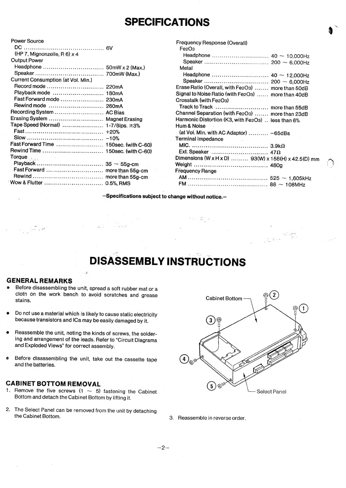
CABINET
BOTTOM
REMOVAL
1.
Remove
the
five
screws
(1
~
5)
fastening
the
Cabinet
Cabinet
Bottom
Select
Panel
Bottom
and
detach
the
Cabinet
Bottom
by
lifting
it.
2.
The
Select
Panel
can
be
removed
from
the
unit
by
detaching
the
Cabinet
Bottom.
3.
Reassemble
in
reverse
order.
o