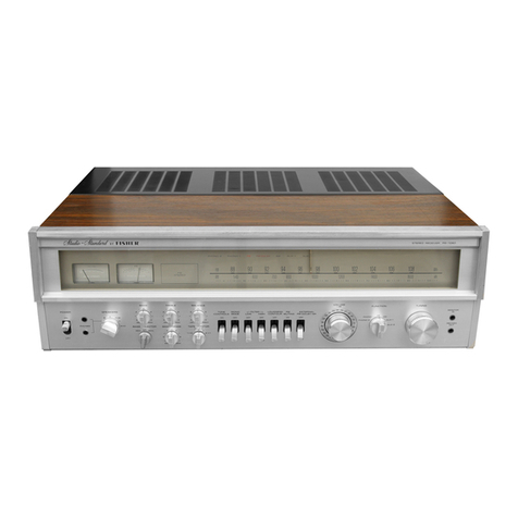
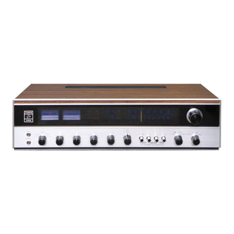
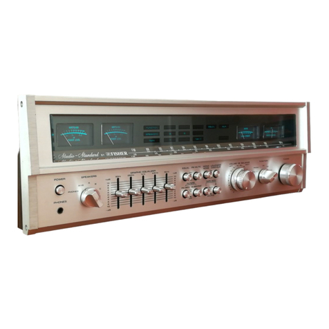
Fisher CR-5125 User manual

SERVICE
MANUAL
FISHER
CR-5125
_
Stereo
Cassette
Tape
Deck
with
Double
Dolby,
Three
Heads
and
Remote
Pause
Control
The
First
Name
in
High
Fidelity

CONTENTS
SPEGIFIGATIONS
232.202
0b
oeccd,
BER
a
a
aS
See
Bate
tea
Hie
kaw
See
eee
dee
ees
3
DISASSEMBEEY,
esr
xctec
8-6-6
wha
ccepiars
Sooke
oid
awe
e
eee
LE
ed
OPES
4-6
MECHANICAL
ADJUSTMENTS
.......
2.0.00.
eee
teens
7&8
ELECTRICAL
ADJUSTMENTS
.......
ccc
ce
te
eee
ee
nena
9-14
REMOTE
CONTROL
ADJUSTMENT
Received
Frequency
Adjustment
..........
0000
cece
eee eee
ee
ee
teenies
15
REMOTE
CONTROL
TRANSMITTER
Transmitted
Frequency
Adjustment...........
000
ccc
cece
cee
eee
eens
16
Transmitter
Parts
List...
0...
0...
ee
ence
een
eeaneeees
17
Remote
Control
Transmitter
Exploded
View
..........
0.000
c
ee
eee
eee
n
ee
neee
17
Transmitter
Schematic
Diagram
.......
0...
0c
cc
eee
eee
eee
eens
18
Transmitter
P.C.Board
(Top
&
Bottom
Views)
.............00
cc
cece
eee
eeeees
18
PARTS.
EIST
vice
oc
eestg
Set
ris
alee
atk
Cee
nes,
Shae
eis:
eee
lw
he ee
19
—25
EXPLODED
VIEW
(CABINET)
........
0...
c
ce
eee
ee
eee
eee
teens
26
EXPLODED
VIEW
(CHASSIS
-1)
1.0.0.0...
cece
cee
ee
eee
ee
eee
eanae
27
EXPLODED
VIEW
(CHASSIS
-2)
..
0...
0...
ccc
eee
enen
eee
eeees
28
EXPLODED:
VIEW
(CHASSIS
33
TOp)
63.5.9
65.06
He
of
escee
dace
op
ack
dee
ee
ae
bie
29
EXPLODED
VIEW
(CHASSIS
4
Bottom)
.........
0.0.0:
cece
eee
ee
eee
eens
30
BLOCK
DIAGRAM)
josie
ie
tea
nwt
Ou
eee
a
nek
otra
etree
eet
wee
wc
31
&
32
DOLBY
NR
UNIT
SCHEMATIC
DIAGRAM
..........
0.00
e
cece
eee
eee
eens
33
DOLBY
NR
UNIT
P.C.BOARD
(TOP
&
BOTTOM
VIEWS)
..........0
0.
cece
ene
33
RECORD
EQ.
UNIT
SCHEMATIC
DIAGRAM
..........
00.0
c
eee
e
eee
ee
eeee
34
RECORD
EQ.
UNIT
P.C.BOARD
(TOP
&
BOTTOM
VIEWS)
..............-0.000-
34
POWER
SUPPLY
P.C.BOARD
(TOP
&
BOTTOM
VIEWS)
............00
cee
eeeee
.
35
CONTROL
AMPLIFIER
P.C.BOARD
(TOP
&
BOTTOM
VIEWS)
..................
36
WIRING
DIAGRAM
(CONTROL
SECTION)
..........
00.
cece
eee
eee
eee
37
&
38
SCHEMATIC
DIAGRAM
(CONTROL
SECTION)
.........
0.02.
ee
ee
eens
39
&
40
AMPLIFIER
BASE
P.C.BOARD
TOP
VIEW
..........
000
eee
eee
eee
eee
41
&
42
AMPLIFIER
BASE
P.C.BOARD
BOTTOM
VIEW
...........
00:
cece
ee ee
nent
43
&
44
WIRING
DIAGRAM
(AMPLIFIER
SECTION)
..............
200:
cee
eee
eeee
45
&
46
SCHEMATIC
DIAGRAM
(AMPLIFIER
SECTION)
...........
Satish
dilate
ged
tee
47
&
48
TRANSISTOR
LEAD
IDENTIFICATION
..........
00
cece
eee
eee
ee
eee
nes
49

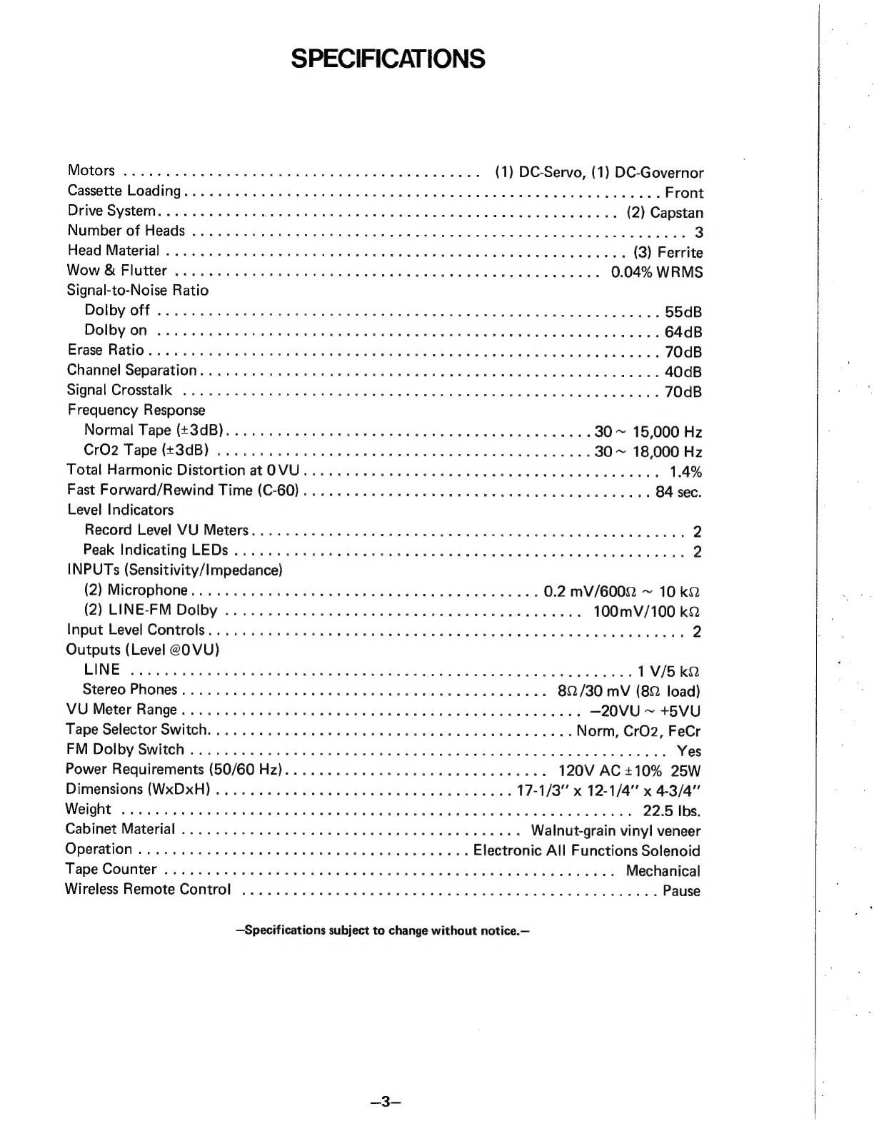
SPECIFICATIONS
Motors
™icisi
ou)
see
Sind
toler,
iar
eect
ateane
ss
hatalis
tod
eosin
(1)
DC-Servo,
(1)
DC-Governor
Cassette
LOad
in
%1g
5x56
toad,
Diced
Rae
bie
EAE
a
og
ASO
awn
ed
wD
RES
Rae
Front
UWE
SYSteM
pies
mas
eee
b
aa
cone
Aone
N
bart
wee
and
bake
ote
eaea
eee
(2)
Capstan
NGmberor
heads
44:5
Awl
neseatea
oe
Geek
aay
ao
eee
chew
eda
data nase
dsiternee
aired
3
Plead
Material
sits
Ged
give
lne
tay
Wace
bdo
pre
teh
ee
ee
ta
ea
gen
Sr
tetas
Shae
ace
(3)
Ferrite
WoW
Plutier
wocces
coe
eos
Bee
aca
ne
eer
alee
yew
een
ee
Od
heeds
0.04%
WRMS
Signal-to-Noise
Ratio
DOIDY
OF
u.8
cents
Stal
Shee
ahaa
aw
tenerk
Bae
yh
Sala
goed
cuahadme
ee
eta
t
55dB
DOIDY:
OW.
syle
Sree
eet
ln
ee
eee
ee
awe
hale
es
Rae
ee
tats
64dB
EraSO:
PROTO:
cal
A
hae
op
i
hates
ge
Se
eater
ee
alee
Caan
args
Slate
haens
aia
aches
toes
ty
70dB
Channel
Separation:
oo,
42-035
ara
4
94s
Ses
winded
ete
wae
Ke
AS
ESAS
he
wee
40cB
BiGlial
ChOSStANC:
505.5..2:
aucoie
uae
eeck
eae
te
Woe
Mearaa
eave
Abe
wlan atte
tea
ahve
dels
Rew
tee
70dB
Frequency
Response
Normal.
Tape
(+3dB)s5
occ
oodcsa
isd
vans
veotind
taba
bones
eee
30
~
15,000
Hz
CrOo-lape(23dB)
i
aocs
onc
de
segma
he
tie
we
ok
ay
tee
wee
td
Sen wed
30
~
18,000
Hz
Total
Harmonic
Distortion
atOVU...
0...
ec
ee
ee
ene
ene
naenaeas
1.4%
Fast
Forward/Rewind
Time
(C-60)..........
00.0
cece
cece
cee
eee
cereeeeeueae
84
sec.
Level
Indicators
Record
Level
VU
Meters...
cc.
dissec
daasen
a
aete
teu
weasa
de
oad
yA
oe
ede
peewee.
2
Peak
Indicating
LEDS:
vec
354
<
Sager
hh
hey
et
wa
cedary
bow
Bua
cigh
ce
ene
Sereda
dian
Barges
2
INPUTs
(Sensitivity/Impedance)
(2)
MICKOPHONG
4.0
2.2.62
tease
aR
each
wie
tate
Roe
eee
weeps
dele
wey
0.2
mV/6002
~
10
kQ
(2)
EINE
BM
D6IBY
a2
&
cs
Gres
vin
te
exceed
a
Mewes
ao
ores
Wis
ate
100mV/100
kQ
Input-Level'Controlsino
sais
Wa
Dew
SS
eee
Fee
e
oso
aw
wow
Swe
DG
sue
ees
aks
2
Outputs
(Level
@0
VU)
LUNE
ics
sarin
erene
ute
&
Rasabu
See
ale
aati
«aed
's
aetna
area
ek
ee
a
Oe
RE
1
V/5
kQ
SIbEO
PRONES
25
5.vecb
cucu
alone
Beare
Oe
e
eS
oan
eae
IS
82/30
mV
(82.
load)
VU
Meter
Range
y
iscsiaccccsine
Ste
ota
ie
alice
Ff
ante
aie
whee
o
widaw
dial
eeetae
ews
—20VU
~
+5VU
Tape
Selector
Switch.
...
0.00.00.
cece
cee
eee
eee
een
nee
eunus
Norm,
CrO2,
FeCr
FIM
Dolby:
SWE
Rit
0c
ena
tidgul
he
Mee
anid
sca
hans
ice
dN
he
Sk
end
alta
ee
ee
Yes
Power
Requirements
(50/60
Hz)...
.......
0.00
cc
cee
eee
eee
neces
120V
AC
+10%
25W
Dimensions
(WxDxH)
....
0.2.0...
cece
eect
e
eee
e
en
eees
17-1/3”
x
12-1/4"
x
4-3/4"
WEIGHS
<cieodmaia
Grvere
wea
ek
x
Dee
Pompey
eee
ate
al
6
a
a
eh
Ms
cosan
22.5
Ibs.
Cabinet
Material.
ycctcene
nye
weacud
ta
oeu
seb
le
tee
HEE
SOR
ROE
Walnut-grain
vinyl
veneer
Operation’.
cic
sett
amie
ee
ee
oS
VEEN
a
Rho
whois
Electronic
All
Functions
Solenoid
(Pape
COUNLEE
3
aaa
ke
ais
arcu
cane
ant
baad
Lee
taled
oad
hah
peda
meted
t
Mechanical
Wireless:
Remote
Control
05
2.5
oasis
ve
vetoed
Sa
ea
Gao
wee
re
Daas
ee
ee
bale
Pause
—Specifications
subject
to
change
without
notice.—

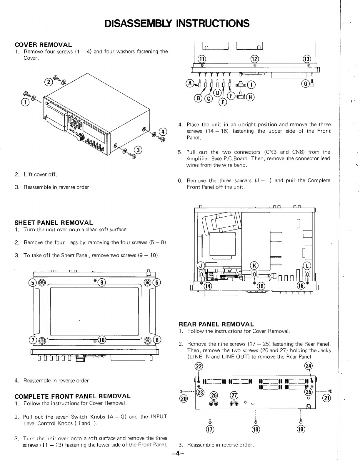
DISASSEMBLY
INSTRUCTIONS
COVER
REMOVAL
1.
Remove
four
screws
(1
—
4)
and
four
washers
fastening
the
Cover.
2.
Lift
cover
off.
3.
Reassemble
in
reverse
order.
SHEET
PANEL
REMOVAL
1.
Turn
the
unit
over
onto
a
clean
soft
surface.
2.
Remove
the
four
Legs
by
removing
the
four
screws
(5
—
8).
3.
To
take
off
the
Sheet
Panel,
remove
two
screws
(9
—
10).
.—
=(9)
4.
Reassemble
in
reverse
order.
COMPLETE
FRONT
PANEL
REMOVAL
1.
Follow
the
instructions
for
Cover
Removal.
2.
Pull
out
the
seven
Switch
Knobs
(A
—G)
and
the
INPUT
Level
Control
Knobs
(H
and
I).
3.
Turn
the
unit
over
onto
a
soft
surface
and
remove
the
three
screws
(11
—
13)
fastening
the
lower
side
of
the
Front
Panel.
@
@)
(2)
®
@DARKAK
eee
see
A®
4.
Place
the
unit
in
an
upright
position
and
remove
the
three
screws
(14—
16)
fastening
the
upper
side
of
the
Front
Panel.
Ohi
5.
Pull
out
the
two
connectors
(CN3
and
CN8)
from
the
Amplifier
Base
P.C.Board.
Then,
remove
the
connector
lead
wires
from
the
wire
band.
6.
Remove
the
three
spacers
(J
—
L)
and
pull
the
Complete
Front
Pane!
off
the
unit.
REAR
PANEL
REMOVAL
1.
Follow
the
instructions
for
Cover
Removal.
2.
Remove
the
nine
screws
(17
—
25)
fastening
the
Rear
Panel.
Then,
remove
the
two
screws
(26
and
27)
holding
the
Jacks
(LINE
IN
and
LINE
OUT)
to
remove
the
Rear
Panel.
Ta
|
|e
||
ree
a
®
@
i
||
ae
A
-
@@
P=
On—
3.
Reassemble
in
reverse
order.
—4~—

DISASSEMBLY
INSTRUCTIONS
(continued)
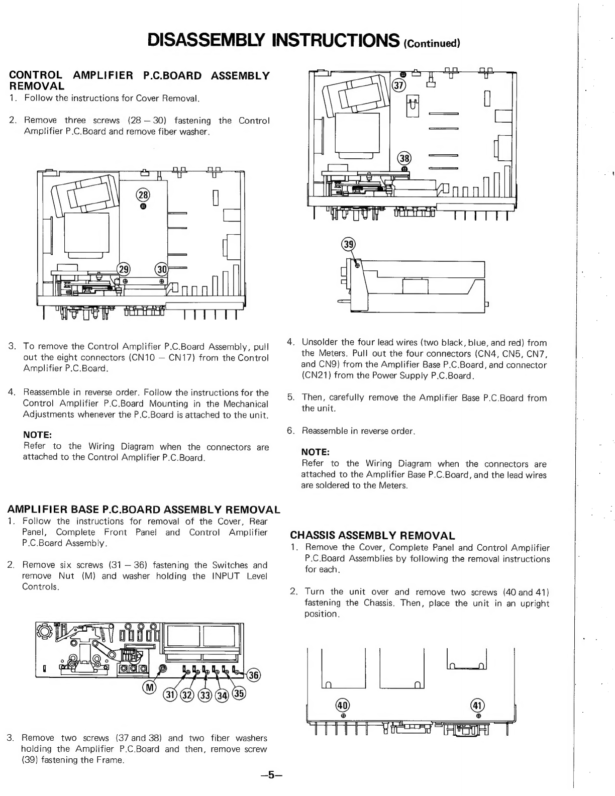
CONTROL
AMPLIFIER
P.C.BOARD
ASSEMBLY
REMOVAL
1.
2.
Remove
three
screws
AMPLIFIER
BASE
P.C.BOARD
ASSEMBLY
REMOVAL
1.
3.
Follow
the
instructions
for
Cover
Removal.
(28
—
30)
fastening
the
Control
Amplifier
P.C.Board
and
remove
fiber
washer.
.
TO
remove
the
Control
Amplifier
P.C.Board
Assembly,
pull
out
the
eight
connectors
(CN10
—
CN17)
from
the
Control
Amplifier
P.C.Board.
Reassemble
in
reverse
order.
Follow
the
instructions
for
the
Control
Amplifier
P.C.Board
Mounting
in
the
Mechanical
Adjustments
whenever
the
P.C.Board
is
attached
to
the
unit.
NOTE:
Refer
to
the
Wiring
Diagram
when
the
connectors
are
attached
to
the
Control
Amplifier
P.C.Board.
Follow
the
instructions
for
removal
of
the
Cover,
Rear
Panel,
Complete
Front
Panel
and
Control
Amplifier
P.C.Board
Assembly.
Remove
six
screws
(31
—
36)
fastening
the
Switches
and
remove
Nut
(M)
and
washer
holding
the
INPUT
Level
Controls.
al
oe
Remove
two
screws
(37
and
38)
and
two
fiber
washers
holding
the
Amplifier
P.C.Board
and
then,
remove
screw
(39)
fastening
the
Frame.
a
ae
.
Unsolder
the
four
lead
wires
(two
black,
blue,
and
red)
from
the
Meters.
Pull
out
the
four
connectors
(CN4,
CN5,
CN7,
and
CNQ)
from
the
Amplifier
Base
P.C.Board,
and
connector
(CN21)
from
the
Power
Supply
P.C.Board.
.
Then,
carefully
remove
the
Amplifier
Base
P.C.Board
from
the
unit.
.
Reassemble
in
reverse
order.
NOTE:
Refer
to
the
Wiring
Diagram
when
the
connectors
are
attached
to
the
Amplifier
Base
P.C.Board,
and
the
lead
wires
are
soldered
to
the
Meters.
CHASSIS
ASSEMBLY
REMOVAL
his
Remove
the
Cover,
Complete
Panel
and
Control
Amplifier
P.C.Board
Assemblies
by
following
the
removal
instructions
for
each.
2.
Turn
the
unit
over
and
remove
two
screws
(40
and
41)
fastening
the
Chassis.
Then,
place
the
unit
in
an
upright
position.

DISASSEMBLY
INSTRUCTIONS
(continued)
3.
Remove
six
screws
(31
—
36)
fastening
the
Switches,
and
remove
Nut
(M)
and
washer
holding
the
INPUT
Level
Controls.
4,
Remove
four
screws
(42
—
45)
fastening
both
sides
of
the
Chassis.
5.
Unsolder
the
five
lead
wires
(two
black,
blue,
red,
and
gray)
from
the
Meters
and
pull
out
the
four
connectors
(CN4,
CN5,
CN7,
and
CN9}
from
the
Amplifier
Base
P.C.Board,
and
the
two
connectors
(CN22
and
CN23)
from
the
Power
Supply
P.C.Board.
6.
Pull
the
Chassis
Assembly
off
the
unit.
7.
Reassemble
in
reverse
order.
NOTE:
Refer
to
the
Wiring
Diagram
when
the
connectors
are
attached
to
the
Amplifier
Base
P.C.Board
and
the
lead
wires
are
soldered
to
the
Meters.

MECHANICAL
ADJUSTMENTS
CONTROL
AMPLIFIER
P.C.BOARD
MOUNTING
Mount
the
P.C.Board
by
the
following
procedures.
1.
Mount
the
Control
Amplifier
P.C.Board
by
temporarily
tightening
the
three
screws,
so
that
the
Stop
Lever
of
the
Completed
Select
Button
is
located
below
the
Release
Lever
of
the
Function
Switch
as
illustrated.
Control
Amplifier
P.C.Board
Release
Lever
Stop
Lever
Serew
fr
1
j
Cotrol
Amplifier
P.C.Board
move
the
P.C.B.
NOTE:
The
Control
Amplifier
P.C.Board
can
easily
be
slid.
2.
Move
the
P.C.Board
to
bring
each
Select
Button
Lever
into
contact
with
each
switch.
Then,
adjust
the
mounting
position
of
the
P.C.Board
correctly
confirming
that
each
button
except
PAUSE
button
is
securely
locked
by
moving
the
P.C.Board.
Function
Switch
Select
Button
Lever
3.
After
tightening
the
mounting
screws,
try
to
push
the
Select
Buttons
again
and
confirm
that
they
are
securely
locked.
Py
[ae
STOP
SWITCH
POSITION
ADJUSTMENT
1.
Push
one
of
the
Select
Buttons
and
lock
it.
Then,
gradually
push
the
STOP
button.
The
Select
Button
should
be
released
after
the
Stop
Switch
is
changed
over.
2.
If
necessary,
loosen
the
screw
fastening
the
Switch
and
adjust
the
position
by
moving
the
Switch
as
illustrated.
Stop
Switch
3.
After
the
adjustment,
tighten
the
screw
and
secure
it
with
paint
or
glue.
NOTE:
Turn
off
the
Power
Switch
whenever
this
adjustment
is
performed.
R/P
SOLENOID
POSITION
ADJUSTMENT
1.
Remove
the
Cover
and
Complete
Front
Panel
by
following
instructions
given
earlier.
Prepare
for
a
spacer
of
0.3mm
as
illustrated.
2.
Loosen
the
two
screws
fastening
the
Solenoid
and
insert
the
spacer
in
the
Solenoid
as
illustrated.
Then,
set
the
unit
in
the
playback
mode
by
pushing
the
PLAY
button.
R/P
Solenoid
MeseorscEtiosececy
move
the
Solenoid
Adjusting
Hole
Slide
Base

MECHANICAL
ADJUSTMENTS
(Continued)
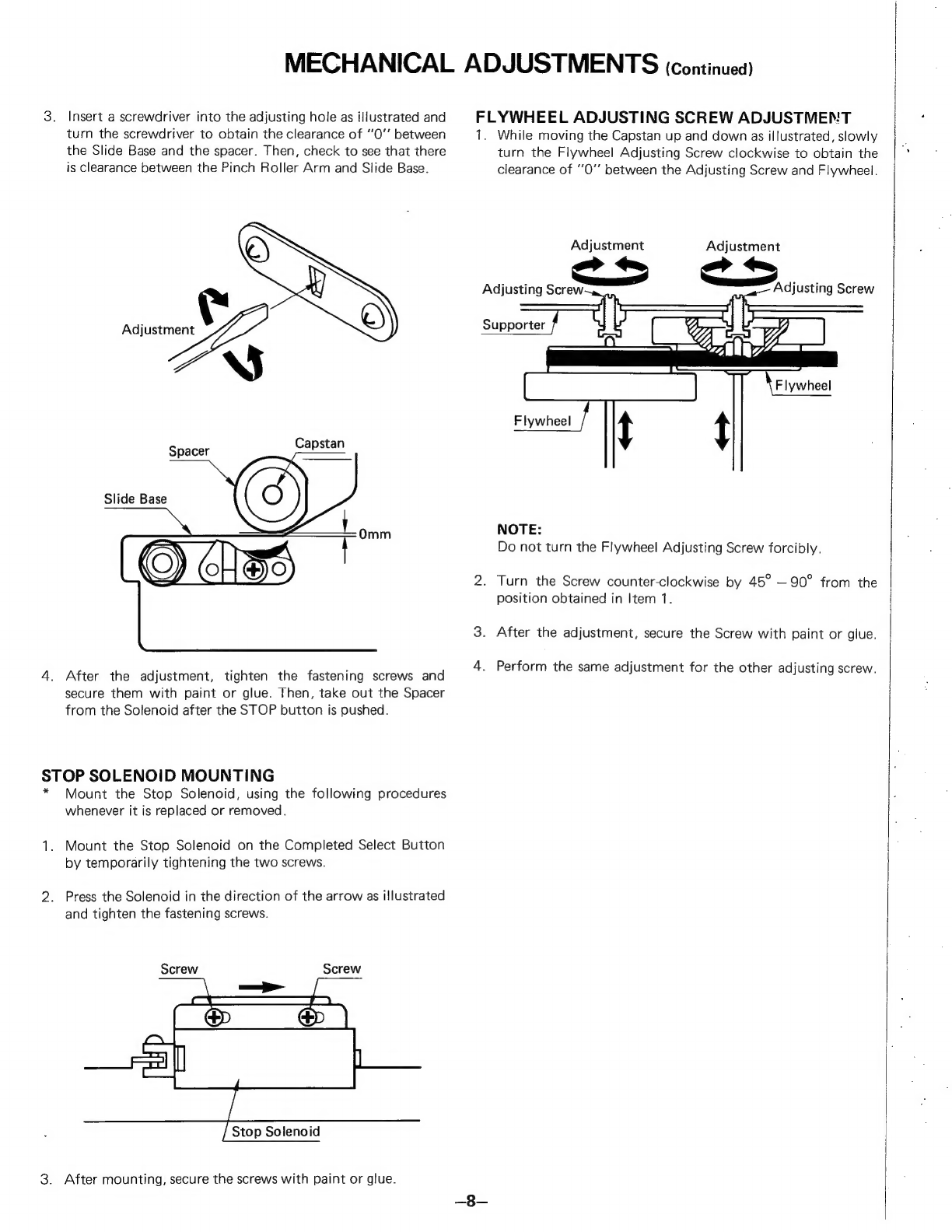
3.
Insert
a
screwdriver
into
the
adjusting
hole
as
illustrated
and
turn
the
screwdriver
to
obtain
the
clearance
of
“‘0’’
between
the
Slide
Base
and
the
spacer.
Then,
check
to
see
that
there
is
clearance
between
the
Pinch
Roller
Arm
and
Slide Base.
Adjustment
ANS
Capstan
Spacer
Slide
Base
()
CHES
4.
After
the
adjustment,
tighten
the
fastening
screws
and
secure
them
with
paint
or
glue.
Then,
take
out
the
Spacer
from
the
Solenoid
after
the
STOP
button
is
pushed.
STOP
SOLENOID
MOUNTING
*
Mount
the
Stop
Solenoid,
using
the
following
procedures
whenever
it
is
replaced
or
removed.
1.
Mount
the
Stop
Solenoid
on
the
Completed
Select
Button
by
temporarily
tightening
the
two
screws.
2.
Press
the
Solenoid
in
the
direction
of
the
arrow
as
illustrated
and
tighten
the
fastening
screws.
Screw
Screw
Stop
Solenoid
3.
After
mounting,
secure
the
screws
with
paint
or
glue.
FLYWHEEL
ADJUSTING
SCREW
ADJUSTMENT
1.
While
moving
the
Capstan
up
and
down
as
illustrated,
slowly
turn
the
Flywheel
Adjusting
Screw
clockwise
to
obtain
the
clearance
of
’’0’’
between
the
Adjusting
Screw
and
Flywheel.
Adjustment
a
Adjusting
Screw
Adjustment
cs.
djusting
Screw
Supporter
Flywheel
NOTE:
Do
not
turn
the
Flywheel
Adjusting
Screw
forcibly.
2.
Turn
the
Screw
counter-clockwise
by
45°
—
90°
from
the
position
obtained
in
Item
1.
3.
After
the
adjustment,
secure
the
Screw
with
paint
or
glue.
4.
Perform
the
same
adjustment
for
the
other
adjusting
screw.

ELECTRICAL
ADJUSTMENTS
REQUIRED
EQUIPMENT
VTVM
Frequency
Counter
Audio
Signal
Generator
Attenuator
Dummy
Load
(47
k-ohm)
Dual-phenomenon
Synchroscope
Test
Tapes
*
3kHz
test
tape
(Example:
TEAC
MTT-111)
for
Tape
Speed
Adjustment
*
10kHz
test
tape
(Example:
TEAC
MTT-114)
for
Head.
Azimuth
Adjustment
*
Test
Tape
for
Dolby
Level
Calibration
(Example:
TEAC
MTT-150)
in
Playback
Gain
Adjustment
®
Test
Tapes
for
recording
and
playback
operations
*
Norma!
Tape
(Example:
BASF
TP-18LHS
T308S)
Ferrichrome
Tape
(Example:
SONY
DUAD
C-60)
*
Chromium
Dioxide
Tape
(Example:
BASF
TP-18CrO2
C401R)
@
Test
Tapes
for
Tape
Running
Condition
Adjustment
*
TDK
SA
C-90
*
MAXELL
UDXLII
C-90
@
Alignment
Tool
Prior
to
the
Electrical
Adjustments,
set
the
unit
and
the
measuring
instruments
as
follows:
*
Dolby
FM
Switch
..........
0.0.00.
00 00
eee
OFF
*
Dolby
NR
Switch
......02..2...
02.00.0000
ee
OFF
*
Bias
Switch.
...........200000-
ee
ee
LOW
*
Equalizer
Switch
..............00000ee
NORMAL
*
Input
Select
Switch
2...
.....
0.00000
eee
LINE
*
Monitor
Switch...
0.0.0...
00. cee
ee
ee
ee
TAPE
*
Audio
Signal
Generator.............
1kHz0dB,1V
NOTE:
The
Electrical
Adjustments
should
be
performed
in
the
order
as
below.
TAPE
SPEED
ADJUSTMENT
1.
Remove
the
Cover
from
the
unit
and
connect
a
frequency
counter
to
the
left
or
right
channel:-LINE
OUT
as
illustrated.
LINE
OUT
PLAY
BACK
Frequency
Counter
3
kHz
(+5
Hz)
2.
Play
back
a
3kHz
test
tape
(Example:
TEAC
MTT-111).
Then,
adjust
the
potentiometer
inside
capstan
motor
by
turning
it
while
the
test
tape
is
being
played
back
until
the
frequency
counter
reading
becomes
3
kHz
(+5
Hz).
Em
HEAD
AZIMUTH
&
TAPE
RUNNING
CONDITION
ADJUSTMENT
ils
wo
Prepare
for
the
two
test
tapes
as
described
below
for
the
Tape
Running
Condition
Adjustment.
We
recommend
“TDK
SA
C-90
and
MAXELL
UDXLII
C-90
cassette
tapes’’
for
this
adjustment.
Cassette
Connect
a
dualtrace
synchroscope
to
both
Left
and
Right
channels
of
LINE
OUT
as
illustrated.
Then,
set
the
synchroscope
as
follows:
®
IMODEN
Snes
asian
teens
Bob
heats
CHOP
(chopped)
*
“SOURCE
42...
woh
owe
as
INT
(internal),
CH1
or
CH2
*
SWEEP’
MODE®
3
<:
ceed
cs
eae
os
AUTO
(automatic)
Synchroscope
Dummy
Load
LINE
OUT
PLAY
BACK
NOTE:
Adjust
the
field
on
the
synchroscope
with
the
VOLT.
ADJ.
and
TIME
ADJ.
Remove
the
Head
Cover
from
the
unit.
Then,
remove
the
Pinch
Roller
of
the
supply
side
by
unscrewing
the
adjusting
nut.

4.
Insert
the
two
test
tapes
into
the
cassette
compartment
alternately
and
play
them
back.
Then,
check
to
see
that
the
tape
is
not
curling
along
the
Tape
Guide
of
the
Combination
ELECTRICAL
ADJUSTMENTS
(continued)
(Record/Playback)
Head
as
illustrated.
Pinch
Roller
(Supply
side)
Tape
Tape
Guide
Tape
Guide
Tape
NOTE:
Replace
the
Pinch
Roller
of
the
Take-up
side
with
a
new
one
Abnormal
Normal
if
a
tape
curl
is
caused.
Insert
the
10
kHz
test
tape
(Example:
TEAC
MTT-114)
into
the
cassette
compartment
and
turn
the
Azimuth
Adjusting
Screw
until
the
waveforms
of
the
Right
and
Left
channels
are
superimposed.
Set
to
optimum
at
maximum
reading
of
the
VTVM.
Adjustment
Azimuth
Adjusting
Screw
6.
Attach
the
Pinch
Roller
of
the
take-up
side
to
the
unit
and
play
back
the
test
tapes
for
the
Tape
Running
Condition
Adjustment.
Then,
adjust
the
Pinch
Roller
height
by
turning
the
adjusting
nut
until
the
tape
is
exactly
centered
in
the
Tape
Guide
of
the
Combination
Head.
7.
While
the
10
kHz
test
tape
(Example:
TEAC
MTT-114)
is
being
played
back,
turn
the
adjusting
nut
until
the
waveforms
of
the
Right
and
Left
channels
are
superimposed.
Set
to
optimum
at
maximum
reading
of
the
VT
VM.
Adjustment
2s
Adjusting
Nut
Pinch
Roller
(Supply
side)
8.
Then,
re-check
to
see
that
the
tape
is
not
curling
along
the
Tape
Guide
of
the
Combination
Head
while
the
test
tapes
for
the
Tape
Running
condition
are
being
played
back.
*
|f
necessary,
turn
the
adjusting
nut
until
the
tape
is
exactly
centered
in
the
Tape
Guide
of
the
Combination
Head.
Adjustment
&
Ss
Adjusting
Nut
Pinch
Roller
(Supply
side)
Tape
Guide
Tape
Vy
Abnormal
Normal
—10—
i
{

ELECTRICAL
ADJUSTMENTS
(Continued)
9.
While
the
10
kHz
test
tape
is
being
played
back
again,
check
to
see
that
the
phase
difference
of
the
Right
and
Left
channels
is
#90°
on
the
synchroscope.
A.
While
the
test
tape
is
playing,
turn
the
azimuth
adjusting
screw
until
the
waveforms
of
the
Right
and
Left
channels
are
superimposed.
Adjustment
y~
Combination
Head
B.
If
not,
replace
the
Pinch
Roller
of
the
take-up
side
wit
AMPLIFIER
GAIN
ADJUSTMENT
h
the
other
one
and
perform
the
adjustment
from
Item
6.
10.
After
the
adjustment,
secure
the
azimuth
adjusting
screw
with
paint
or
glue.
AT
LEFT
CHANNEL
Connect
an
audio
signal
generator
and
an
attenuator
to
the
jeft
channel
LINE
IN,
a
VTVM
to
the
test
point
(TP101),
and
a
VTVM
to
the
left
channel
LINE
OUT
as
illustrated.
Audio
Signal
Generator
TINE
IN
RECORD
Attenuator
200mvV
(—14
dB)
VTVM
(580
mV)
Dummy
Load
Set
the
Monitor
Switch
to
SOURCE
and
feed
the
1
kHz
signal
from
the
audio
signal
generator
at
200
mV
(—14
dB)
to
the
unit.
Adjust
the
left
channel
INPUT
Level
Control
until
the
output
level
on
the
test
point
(TP101)
becomes
580
mV
on
the
VTVM.

ELECTRICAL
ADJUSTMENTS
(Continued)
4.
Then,
adjust
the
potentiometer
(P103)
until
the
output
Jevel
of
1
V
on
the
LINE
OUT
is
obtained
on
the
VTVM
keeping
the
unit
in
the
above
condition.
RIGHT
CHANNEL
Connect
an
audio
signal
generator
to
the
right
channel
LINE
IN,
a
VTVM
to
the
test
point
(TP201),
anda
VTVM
to
the
right
channel
LINE
OUT.
Then,
adjust
the
right
channel
INPUT
Level
Control
and
the
potentiometer
(P203)
for
the
right
channel
by
following
the
same
procedure
as
for
the
left
channel.
PLAYBACK
GAIN
&
METER
LEVEL
ADJUSTMENT
LEFT
CHANNEL
1.
Connect
a
VTVM
to
the
left
channel
LINE
OUT
as
illustrated.
Then,
insert
a
test
tape
for
the
DOLBY
Level
calibration
(Example:
TEAC
MTT-150)
into
the
cassette
compartment.
LINE
OUT
PLAY
BACK
VTVM
(1V)
ND
47
k-ohm
Dummy
Load
2.
While
the
test
tape
is
being
played
back,
adjust
the
potentiometer
(P107)
until
the
output
level
becomes
71
V
on
the
VTVM.
3.
Keeping
the
unit
in
the
playback
mode,
adjust
the
potentiometer
(P102)
until
the
pointer
of
the
left
channel
Meter
swings
to
+3VU
(DOLBY
mark
position)
as
illustrated.
[4]
FISHER
INPUT
LEVEL
/OUTPUT
ZEVEL
RIGHT
CHANNEL
Connect
a
VTVM
to
the
right
channel
LINE
OUT.
Then,
adjust
the
potentiometers
(P207
and
P202)
for
the
right
channel
by
following
the
same
procedure
as
for
the
left
channel.
DOLBY
FM
SENSITIVITY
ADJUSTMENT
LEFT
CHANNEL
1.
Connect
an
audio
signal
generator
and
an
attenuator
to
the
left
channel
LINE
IN,
and
a
VTVM
to
the
left
channel
LINE
OUT
as
illustrated.
Audio
Signal
Generator
1
kHz
1V
RMS
RECORD
Attenuator
200mV
(—14
dB)
VTVM
(1V)
Dummy
Load
Left
Channel
Output
=
Right
Channel
Output
2.
Set the
DOLBY
FM
Switch
to
ON,
and
the
Monitor
Switch
to
SOURCE.
Then,
feed
the
1
kHz
signal
from
the
audio
signal
generator
at
200
mV
(—14
dB)
to
the
unit
with
the
DOLBY
FM
Sensitivity
Control
set
to
the
maximum.
3.
Read
the
output
level
on
the
VTVM.
RIGHT
CHANNEL
Feed
the
1
kHz
signal
from
the
audio
signal
generator
at
200
mV
(—14
dB)
to
the
right
channel
LINE
IN
and
adjust
the
potentiometer
(P201)
until
the
output
level
of
right
channel
becomes
identical
to
the
left
channel
output
level
on
the
VTVM.
LINE
IN—;

ELECTRICAL
ADJUSTMENTS
(continued)
RECORDING
BIAS
ADJUSTMENT
for
Chromium
Dioxide
Tape
LEFT
CHANNEL
Connect
an
audio
signal
generator
and
an
attenuator
to
the
left
channel
LINE
IN,
and
a
VTVM
to
the
left
channel
LINE
OUT
as
illustrated.
Then,
insert
a
chromium
dioxide
tape
into
the
cassette
(Example:
BASF
TP-18CrO2
C401R)
compartment.
Audio
Signal
Generator
1kHz
1V
RMS
Attenuator
10
mV
(—40
dB)
Dummy
Load
1
kHz=14
kHz
(+1
dB)
Set
the
Equalizer
Switch
to
CrO2,
and
the
Bias
Switch
to
HIGH.
Set
the
Monitor
Switch
to
TAPE
and
feed
the
1
kHz
signal
from
the
audio
signal
generator
at
10
mV
(—40
dB)
to
the
unit
with
the
INPUT
Level
Control
set
to
the
maximum.
Then,
set
the
unit
in
the
recording
mode
and
read
the
output
level
on
the
VTVM.
.
While
the
signal
is
being
recorded,
change
the
audio
signal
generator
from
the
1
kHz
signal
to
the
14
kHz
signal.
Then,
check
that
the
14
kHz
signal
output
level
is
identical
to
the
1
kHz
signal
output
level
or
the
deviation
is
+1
dB
on
the
VTVM.
If
not,
adjust
the
potentiometer
(P7109)
and
re-check
the
outputs
of
each
signal
by
alternately
changing
the
audio
signal
generator
to
the
1
kHz
signal
and
the
14
kHz
signal.
Repeat
the
above
adjustment
until
the
specified
output
is
obtained.
RIGHT
CHANNEL
Connect
an
audio
signal
generator
and
an
attenuator
to
the
right
channel
LINE
IN,
and
a
VTVM
to
the
right
channel
LINE
OUT.
Then,
adjust
the
potentiometer
(P209)
for
the
right
channel
by
following
the
same
procedure
as
for
the
left
channel.
e
For
Ferrichrome
Tape
Set
the
Switches
as
follows:
*
Equalizer
Switch
*
Bias
Switch
Then,
insert
a
ferrichrome
tape
(Example:
SONY
DUAD
C-60)
into
the
cassette
compartment.
Adjust
the
potentiometers
by
following
the
conditions
described
below
and
the
same
procedure
as
for
the
Chromium
Dioxide
Tape.
*
Input
Signals
1
kHz
and
14
kHz
Sl
nput
evel
4
saree
eens
BUA
Me
10
mV
(—40
dB)
*
Potentiometers
for
adjustment
Lettiichannel:
ce
2ekck
ou
Daesuk
ed
wits
GS
ow
OB
P108
Rightschannel
0
fo
ete
he
eee
wena
P208
e
For
Normal
Tape
Set
the
Switches
as
follows:
*
Equalizer
Switch
...............0...0..
Fe203
*
Blas:
SWITCH
tn
omits
do
Oh
cae
de
eae
Oe
a
Vleck
LOW
Then,
insert
a
normal
tape
(Example:
BASF
TP-18LHS
T308S)
into
the
cassette
compartment.
Adjust
the
potentiometers
by
following
the
conditions
described
below
and
the
same
procedure
as
for
the
Chromium
Dioxide
Tape.
*
Input
Signal...
2.
1
kHz
and
13
kHz
*
put
LOVE)
ve.
5
ob
Sow
eae
Bee
we
10
mV
(—40
dB)
*
Potentiometers
for
adjustment
eft:channe!
oud
new
bhi
Pas
ee
ede
he
es
P110
Right:channel
4.4
2.8.06
ek
ee
a
ke
oo
ed
eee
P210
RECORDING
GAIN
ADJUSTMENT
e@
For
Chromium
Dioxide
Tape
LEFT
CHANNEL
1.
Connect
an
audio
signal
generator
and
an
attenuator
to
the
left
channel
LINE
IN
as
illustrated.
Then,
insert
a
chromium
dioxide
tape
(Example:
BASF
TP-18CrO2
C401R)
into
the
cassette
compartment.
Audio
Signal
LINE
IN—
RECORD
Generator
1
kHz
1V
RMS
Attenuator
200mV
(—14
dB)
2.
Set
the
Equalizer
Switch
to
CrO2,
and
the
Bias
Switch
to
HIGH.
3.
Set
the
Monitor
Switch
to
SOURCE
and
feed
the
1
kHz
signal
from
the
audio
signal
generator
at
200
mV
(—14
dB)
to
the
unit.

ELECTRICAL
ADJUSTMENTS
(Continued)
4.
Set
the
unit
in
the
recording
mode
and
adjust
the
INPUT
Level
Contro!
until
the
pointer
of
the
left
channe!
Meter
swings
to
O
VU
as
illustrated
while
the
1
kHz
signal
is
being
recorded.
*
FISHER
INPUT
LEVEL/OUJPUT
LEVEL
.
Change
the
Monitor
Switch
from
SOURCE
to
TAPE
and
check
to
see
that
the
pointer
of
the
left
channel
Meter
stays
at
O
VU.
If
not,
adjust
the
potentiometer
(P104)
and
check
the
swing
of
the
pointer.
Repeat
the
above
adjustment
until
the
pointer
of
the
left
channel
meter
stays
at
0
VU.
RIGHT
CHANNEL
Connect
an
audio
signal
generator
and
an
attenuator
to
the
right
channel
LINE
IN.
Then,
adjust
the
potentiometer
(P204)
for
the
right
channel
by
following
the
same
procedure
as
for
the
left
channel.
—-14—
for
Ferrichrome
Tape
Set
the
Switches
as
follows:
*
Equalizer
Switch
*
“Blas
OWitChg.o
2084
gap
Sowa
seth
od
ee
eee
eth
MID.
Then,
insert
a
ferrichrome
tape
(Example
SONY
DUAD
C-60)
into
the
cassette
compartment.
Adjust
the
potentiometers
by
following
the
conditions
described
below
and
the
same
procedure
as
for
the
Chromium
Dioxide
Tape.
*
INpUtSighal:
«0.2
sets
bed
det
ds
oS,
OE
AS
1
kHz
*
INPUT
LEVEl)
init
oo
cokten
cd
Pele
al
ades
os
200
mV
(—14
dB}
*
Potentiometers
for
adjustment
Bettcchaniel.!
26352
nen
2
BAY
bed
oo
we
nes
P106
Right
channel
for
Normal
Tape
Set
the
Switches
as
follows:
*
Equalizer
Switch
®
BIAS
OWITCA
4828.4
Sancho
d
Ao
Oe
aes
Bane
iat
LOW
Then,
insert
a
normal
tape
(Example:
BASF
TP-18LHS
T308S)
into
the
cassette
compartment.
Adjust
the
potentiometers
by
following
the
conditions
described
below
and
the
same
procedure
as
for
the
Chromium
Dioxide
Tape.
S-APUE
SIOMAl
2d.
ec
2
Wes
tee
Ci
Ree
hed
ie
Bn
a
1
kHz
input
Level:
2005
i
die
ea
as
200
mV
(—14
dB)
*
Potentiometers
for
adjustment
Leftchannel
......
20.0.0...
00.00.
ecu
P105
Right
channel
.............0...0..00004
P205

REMOTE
CONTROL
ADJUSTMENT
RECEIVED
FREQUENCY
ADJUSTMENT
Synchroscope
1.
Pull
out
the
two
connectors
(CN18
and
CN19)
from
the
sine
wave
(Max.)
Control
Amplifier
P.C.Board.
2.
Connect
an
audio
signal
generator,
a
SCA
signal
generator,
and
an
attenuator
to
the
connector
pins
(CN18
and
CN19)
and
then,
connect
a
VTVM
and
a
synchroscope
across
Resistor
R515
on
the
Control
Amplifier
P.C.Board
as
illustrated.
Attenuator
1
mV
(—60
dB)
be)
Se
CN18
SCA
Signal
Generator
>
‘
38
kHz,
Deviation
+1
kHz
CN19
7
L823
}
Audio
Signal
Generator
570
Hz
E
ope
3.
Modulate
the
signal
of
570
Hz
produced
from
the
audio
signal
generator
at
38
kHz,
deviation
+1
kHz
in
the
SCA
signal
generator.
4.
Feed
the
modulated
signal
at
1mV(—60dB)
to
the
connector
pin
(CN18)
with
the
unit
in
the
playback
mode.
5.
Turn
the
cores
of
the
transformers
(T501
and
T502)
with
an
Synchroscope
alignment
tool
until
the
signal
sine
wave
becomes
the
sinewave:
(Max:)
maximum
at
peak-to-peak
on
the
synchroscope.
6.
Connect
the
VTVM
to
the
Pin
No.
5
of
C501
as
illustrated.
Then,
adjust
the
potentiometer
(P501)
until
the
VTVM
reading
becomes
the
maximum
while
feeding
the
modulated
signal
to
the
connector
pin
(CN18)
with
the
unit
in
the
playback
mode.
Attenuator
c—__
1
mV
(—60
cB)
ea
=
=
CN18
SCA
Signal
Generator
38
kHz,
Deviation
+1
kHz
CN19
i
é ‘
ta
Audio
Signal
:
|@s
Generator
570
Hz
:
:
ote
ewe
—15—

TRANSISTER
ADJUSTMENT
TRANSMITTED
FREQUENCY
ADJUSTMENT
1.
Connect
a
frequency
counter
through
a
47
k-ohm
resistor
to
the
emitter
of
Transistor
Q2
as
illustrated.
Frequency
Counter
570
Hz
(+3 Hz)
4.
Adjust
the
potentiometer
(P3)
to
obtain
38
kHz
(+0.2
kHz)
on
the
frequency
counter.
Then,
turn
the
core
of
the
transformer
(T1)
until
the
wave
form
becomes
the
maximum
at
peak-to-peak
(50
—
55
V)
on
the
synchroscope
(Volt.
Range:
10V/cm.).
5.
Check
to
see
that
the
frequency
counter
reads
38
kHz
(£0.2
kHz).
*
If
not,
repeat
the
adjustment
in
Item
3
until
the
specified
value
is
obtained.
6.
Connect
the
synchroscope
(Volt.
Range:
0.2V/cm)
to
the
plus
side
of
Capacitor
C6
as
illustrated.
Then,
adjust
the
potentiometer
(P2)
until
the
synchroscope
reading
becomes
1
V
at
peak-to-peak.
Synchroscope
§
1V
‘
—16—
2.
Turn
the
potentiometer
(P2)
fully
counter-clockwise
and
adjust
the
potentiometer
(P1)
by
turning
it
until
the
oscillation
frequency
becomes
570Hz
(+3Hz)
on
the
frequency
counter.
3.
Connect
the
frequency
counter
through
a
47
k-ohm
resistor
and
a
synchroscope
to
the
transmitter
output
as
illustrated.
Synchroscope
50
—
55V
Frequency
Counter
38
kHz
(40.2
kHz)
Resistor
)
(47
k-ohm)
Output
eid
i
wil
en
Cc
—s
\acitfamms
co

TRANSISTER
PARTS
LIST
Description
REMOTE
CONTROL
TRANSMITTER
ASSY
4
1922
00010}
Remote
Control
Transmitter
Assy
103
3
1303
00811]
Screw,
Pan Hd.
Tapping-2.
+M3.0x8
131
0
4001
00110]
Transmitter
P.C.B.
Assy
131
2
7103
33100]
Label
141
2
1119
48100]
Box,
Top
141
2
1119
48200]
Box,
Bottom
141
2
1439
09400)!
Battery
Sheet
141
2
1449
38200]
Box
Plate
141
2
1619
47800]
Button
141
2
2449
25100}
Sheet
141
2
3829
16800]
Battery
Terminal
141
2
4219
13500]
Screw
141
2
4469
25100]
Cushion
141
2
4469
25000}
Cushion
131
2
7103
22600]
Label
TRANSMITTER
P.C.B.
ASSY
CM1
5
3500
KOOSV
|
Mylar
0.015uF
CD10
6100
0000V
|
Electrolytic
10uF
CD10
6100
0000V
|
Electrolytic
10uF
203
5
5100
53670
|
Transistor,
2SC536
203
5
5100
53670
|
Transistor,
2SC536
203
5
5100
53670
|
Transistor,
2SC536
203
5
5100
53670
|
Transistor,
2SC536
203
5
5100
53670
|
Transistor,
2SC536
RD1
8
4251
JVO00|
Carbon
180k
ohm
1/4W
RD2
2
2251
JVO00
|
Carbon
2.2k
ohm
1/4W
RD2
2
0251
JVO000
|
Carbon
22
ohm
1/4W
RD4
7
2251
JV000
|
Carbon
4.7k
ohm
1/4W
RD2
2
2251
JVOO0
|
Carbon
2.2k
ohm
1/4W
RD4
7
2251
JVOO0
|
Carbon
47k
ohm
1/4W
RD4
7
3251
JVO00
|
Carbon
47k
ohm
1/4W
131
2
4203
19600]
Washer
RD2
2
2251
JVO00
|
Carbon
2.2k
ohm
1/4W
TRANSMITTER
P.C.B.
ASSY
RD3
3
1251
JVOOO
|
Carbon
330
ohm
1/4W
RD3
3
1251
JVO00
|
Carbon
330
ohm
1/4W
131
0
4001
001
oe
Transmitter
P.C.B.
Assy
RD2
7
2251
JVOOO
|
Carbon
2.7k
ohm
1/4W
4
1519
70650!
Speaker
(Transmitter)
2.7k
ohm
1/4W
4
2262
01630]
Transmitter
P.C.B.
5.6k
ohm
1/4W
——
Ne
ee
a
a
es
RD2
7
2251
JVOOO
|
Carbon
RD5
6
2251
JVOO00
}
Carbon
4
2312
01060
141
2
3829
22101
141
2
3829
22202
CM4
7
3500
KOOSV
CM4
7
3500
KOOSV
CM4
7
3500
KOOSV
Push
Switch
1
Key
Battery
Terminal
Battery
Terminal
Mylar
0.047
uF
Mylar
0.047
uF
Mylar
0.047
uF
RDS
6
2251
JVOO00
RD1
0
4251
JVOOO
RD5
6
2251
JVO000
RD2
2
0251
JV000
RD3
9
0251
JVO00
RD4
7
3251
JVO0O
Carbon
Carbon
Carbon
Carbon
Carbon
Carbon
5.6k
ohm
100k
ohm
5.6k
ohm
22
ohm
39
ohm
47k
ohm
1/4W
1/4W
1/4W
1/4W
1/4W
1/4W
CM4
7
3500
KOOSV
|
Mylar
0.047
uF
CD3
3
6100
O000V
|
Electrolytic
33
uF
CD2
25250
OOOOV
|
Electrolytic
2.2uF
CM5
6
2500
KOOSV
|
Mylar
0.0056uF
CM5
6
2500
KOOSV
|
Mylar
0.0056yuF
RD1
2
4251
JVOOO
|
Carbon
120k
ohm
1/4W
4
2542
00010
|
Output
Transformer
4
2229
22671
|
Semi-fixed
Resistor
(B-5k)
4
2229
23880
|
Semi-fixed
Resistor
(B-4.7k)
4
2229
22910
|
Semi-fixed
Resistor
(B-1k)
PRPs
swoon
nono
nani
n
REMOTE
CONTROLE
TRANSMITTER
EXPLODED
VIEW
141
2
4219
13500
gs
Screw
141
21119
48200
Box
Bottom
#PTS-2
3x8
“\
131
0
4001
00110
Transmitter
PC
Assy
141
2
1619
47800
Button
141
2
4469
25100
Cushion
PN
Hy
VY
141
2
3829
16800
Terminal
Battery
|
ea
aases
25000
141
2
1439
09400
Battery
Sheet
141
22449
25100
Sheet
141
2
1449
38200
Plate
Box
—~17—

REMOTE
CONTROL
TRANSMITTER
SCHEMATIC
DIAGRAM
,
93,
04,95
2SC536
TRANSMITTER
yk)
B-
KA
ate
REMOTE
CONTROL
TRANSMITTER
PC.BOARD
(Top
View)
(Bottom
View)
TRANSMITTER
re
OS
8
pig
=
Sle:
z
1
aU
Me
oe
S|
PUSH_
SLIDE
SWITCH
—18—

PACKAGE
PARTS
LIST
Description
Part
No.
CABINET
Description
141
6
1449
55000
141
6
1449
55700
141
6
2519
07690
141
6
2519
08490
141
6
2519
10015
141
6
2519
10018
141
6
2519
10022
141
6
3919
36300
141
6
4419
12601
141
6
4559
02300
141
6
4799
14700
141
6
4799
14701
141
6
4799
14702
141
6
4799
14703
141
6
4799
14704
141
6
4799
14705
141
6
1419
ee
Individual
Carton
141
6
1449
52400
|
Styrofoam
Case
Styrofoam
Case
Styrofoam
Pad
Fan
Bag
Poly
Cover
Poly
Cover
Poly
Cover
Poly
Cover
Plain
Pad
Control
Tag
Serial
No.
Sheet
Month
Label,
Brown
(Jan.,
Feb.)
Month
Label,
Red
(Mar.,
Apr.)
Month
Label,
Green
(May,
Jun.)
Month
Label,
Blue
(Jul.,
Aug.)
Month
Label,
Orange
(Sep.,
Oct.)
Month
Label,
Violet
(Nov.,
Dec.)
141
6
4559
00100
|
Serial
No.
Sheet
SPP
See
eae
ones
ooo
oo
os
os
os
131
3
1303
00611
101
3
1304
00811
104
3
1303
01411
143
3
1903
01411
101
3
1303
00511
143
3
1903
00811
143
3
1903
00618
143
3
1903
00818
110
3
1203
00013
101
3
1704
00518
101
3
1303
00611
101
3
1203
00811
101
3
1202
60411
143
3
1903
00618
Screw,
Pan Hd.
C
SW
+M3.0x6
Screw,
Pan
Hd.
+M4.0x8
Screw,
Pan
Hd.
Tapping-3
+M3.0x14
Screw,
Brazier
Hd.
Tapping-2
+M3.0x14
Screw,
Pan Hd.
+M3.0x5
Screw,
Brazier
Hd.
Tapping-2
+M3.0x8
Screw,
Brazier
Hd.
Tapping-2
+M3.0x6
Screw,
Brazier
Hd.
Tapping-2
+M3.0x8
Finished
Washer
M3.0
Screw,
Bind
Hd.
+M4.0x5
Screw,
Pan Hd.
+M3.0x6
Screw,
Flat
Hd.
+M3.0x8
Screw,
Flat
Hd.
+M2,.6x4
Screw,
Brazier
Hd.
Tapping-2
+M3.0x6
ACCESSORIES
PAUSE
INDICATOR
P.C.B.
ASSY
4
1922
00010
4
2369
70571
131
2
7103
27800
131
6
4319
10802
131
6
4519
14400
141
6
4119
77600
141
6
4729
09800
CABINET
141
2
4539
03200
141
2
3119
11000
4
2519
72650
141
2
3719
04400
141
2
3719
04200
141
2
4569
06800
4
2439
70892
141
2
3899
06800
141
2
3899
06900
141
2
3519
38400
141
0
1119
56100
141
2
3529
16801
141
2
1119
50500
141
21119
50400
141
2
4539
12400
141
2
3519
41300
141
2
1259
02400
141
2
1539
10100
141
2
1449
39900
141
2
1249
19000
141
0
1539
00500
141
2
7519
38900
4
2319
73200
4
2239
70220
4
2379
70110
141
2
1149
19102
141
2
1149
19101
141
0
3779
00400
141
2
4469
27900
141
2
4469
26700
141
0
1619
24400
141
2
1619
52900
141
2
1639
26400
141
2
1639
26500
131
2 1801
13200
131
2
4201
17800
143
3
1903
00611
131
3
1303
00511
101
3
1303
00611
Remote
Control
Transmitter
Assy
Patch
Cord
Label
Service
Station
List
Warranty
Card
Instruction
Manual
Caution
Label
Fiber
Washer
Cabinet
Chassis
Power
Transformer
Transformer
Cover
Power
Transformer
Bracket
Washer,
Transformer
Power
Cord
Cord
Holder
Clamp,
Power
Cord
P.C.B.
Bracket
Front
Panel
Complete
Spacer
Rear
Panel
Cover
Washer
Circuit
Bracket
Panel
Sheet
Blind
Blind
Cover
Dust
Cover
Head
Cover
Assy
Snap
Power
Switch
Capacitor
0.01
uv
Solderless
Terminal
Frame
Frame
Support
P.C.B.
Assy
Cushion
Indicator
Cushion
Switch
Knob
Assy
Reset
Button
Knob
Knob
Leg
Screw,
Ground
Screw,
Brazier
Hd.
Tapping-2
+M3.0x6
Screw,
Pan Hd.
C
SW
Screw,
Pan
Hd.
+M3.0x5
+M3.0x6
D517
i
4
2269
30720
4
1329
74220
|
Pause
Indicator
P.C.B.
Assy
4
2029
70720
|
Diode,
SLP-132B
Indicator
P.C.B.
OSPF
PBSFAHSNNNSP
HH
esa
pses
sansa
nn
nwa
saew
oa
pypyasiniga
=
4
1329
74160
141
2
3779
10600
4
2369
71480
4
2369
71850
4
2359
72150
4
2359
72350
4
2369
71850
4
2359
73990
4
2359
74000
4
2359
716000
CC1
0
1500
KEOOC
CMB5
6
3500
KOOSV
CM1
5
3500
KOOSV
CD2
2
563A
0000V
CD1
0
6160
O000V
CD1
0
5160
O000V
CD3
3
663A
O000V
CC1
5
1500
KEOOC
CD1
0
6250
O000V
CD1
0
6250
0000V
CD1
0
6250
0000V
CC4
7
1500
KEOOC
CD1
0
6250
0000V
CD1
0
6250
0000V
CD1
0
5250
O0000V
CD1
05160
O000V
CC4
7
1500
KEOOC
CD1
0
5250
O000OV
CC1
0
1500
KEOOC
CDi
0
6250
0000V
CT1
0
4160
KOODV
CD1
0
763A
O000V
CC4
7
0500
KEOOC
CM1
8
2500
KOOSV
CM1
0
2500
KOOSV
CD3
3
663A
O000V
CD1
0
6250
O000V
CD2
2
5100
0000V
CT1
5
4350
KOODV
CC1
0
1500
KEOOC
CCi1
0
1500
KEOOC
CD1
0
6160
O000V
CC4
7
1500
KEOOC
CDi
0
6160
O000V
AMPLIFIER
BASE
P.C.B.
ASSY
Amplifier
Base
P.C.B.
Assy
P.C.B.
Clamp
Connector
3P
Connector
4P
Connector
9P
Connector
4P
Connector
4P
Connector
3P
Assy
Connector
3P
Assy
Connector
6P
Ceramic
100pF
Mylar
0.056uF
Mylar
0.015pF
Electrolytic
2.
2uF
Electrolytic
10uF
Electrolytic
Tur
Electrolytic
33yuF
Ceramic
150pF
Electrolytic
10uF
Electrolytic
10uF
Electrolytic
10OuF
Ceramic
470pF
Electrolytic
10nF
Electrolytic
10uF
Electrolytic
Tur
Electrolytic
Tur
Ceramic
470pF
Electrolytic
Tur
Ceramic
100pF
Electrolytic
10uF
Tantalum
O.1uF
Electrolytic
100uF
Ceramic
47pF
Mylar
0.0018uF
Mylar
0.0014uF
Electrolytic
S3uF
Electrolytic
10uF
Electrolytic
2.2uF
Tantalum
0.15uF
Ceramic
100pF
Ceramic
7OOpF
Electrolytic
10uF
Ceramic
470pF
Electrolytic
10uF
PSP
PPP
BPP
HP HP
Hesse
sn
nnn
sss
nnn
srs
nnn
cin
ni
gaa

CC3
9
0500
KEOOC
CD1
0
6160
O000V
CD1
0
7250
0000V
CD10
6160
O000V
CC4
7
1500
KEOOC
CDi
0
6160
0000V
CC3
9
0500
KEOOC
CD1
0
6160
O000V
CD4
7
5160
0000V
CC3
9
0500
KEOOC
CC1
0
1500
KEOOC
CM5
6
3500
KOOSV
CM1
5
3500
KOOSV
CD2
2
563A
O000V
CD1
0
6160
0000V
CD1
0
5160
O000V
CD3
3
663A
O000V
CC1
5
1500
KEOOC
CD1
0
6250
O000V
CD1
0
6250
0000V
CD1
0
6250
0000V
CC4
7
1500
KEOOC
CD1
0
6250
OO000V
CD1
0
6250
0000V
CD1
0
5250
0000V
CD1
0
5160
O000V
CC4
7
1500
KEOOC
CD1
0
5250
O000V
CC1
0
1500
KEOOC
CD1
0
6250
O000V
CT1
04160
KOODV
CD10
763A
O000V
CC4
7
0500
KEOOC
CM1
8
2500
KOOSV
CM1
0
2500
KOOSV
CD3
3
663A
O000V
CD1
0
6250
0000V
CD2
2
5100
0000V
CT1
5
4350
KOODV
CC1
0
1500
KEOOC
CC1
0
1500
KEOOC
CD1
0
6160
0000V
CC4
7
1500
KEOOC
CD1
0
6160
O000V
CC3
9
0500
KEOOC
CD1
0
6160
O000V
CD1
0
7250
O000V
CD1
0
6160
0000V
CC4
7
1500
KEOOC
CD1
0
6160
O000V
CC3
9
0500
KEOOC
CD1
0
6160
O0000V
CD4
7
5160
O0000V
CC3
9
0500
KEOOC
CD1
0
7250
0000V
CD10
7160
OO00V
CD4
7
7350
OOO00V
CD2
2
7350
O0000V
CD4
7
6250
0000V
CD10
7160
OOOOV
CD1
0
7350
O0OO0V
4
2029
70160
202
59110
18820
202
5
9110
18820
202
5
9110
18820
4
2029
70160
4
2029
70160
202
5
9110
18820
4
2029
70160
202
5
9110
18820
Ceramic
Electrolytic
Electrolytic
Electrolytic
Ceramic
Electrolytic
Ceramic”
Electrolytic
Electrolytic
Ceramic
Ceramic
Mylar
My
tar
Electrolytic
Electrolytic
Electrolytic
Electrolytic
Ceramic
Electrolytic
Electrolytic
Electrolytic
Ceramic
Electrolytic
Electrolytic
Electrolytic
Electrolytic
Ceramic
Electrolytic
Ceramic
Electrolytic
Tantalum
Electrolytic
Ceramic
Mylar
Mylar
Electrolytic
Electrolytic
Electrolytic
Tantalum
Ceramic
Ceramic
Electrolytic
Ceramic
Electrolytic
Ceramic
Electrolytic
Electrolytic
Electrolytic
Ceramic
Electrolytic
Ceramic
Electrolytic
Electrolytic
Ceramic
Electrolytic
Electrolytic
Electrolytic
Electrolytic
Electrolytic
Electrolytic
Electrolytic
Diode,
18953
Diode,
1$188
Diode,
18188
Diode,
1S188
Diode,
18953
Diode,
1S953
Diode,
18188
Diode,
1$953
Diode,
18188
39PF
10uF
100uF
10uF
470PF
1OuF
S9OPF
10uF
4.7
pF
39PF
100PF
0.056uF
0.015uF
2.2uF
10uF
Woe
33uF
150pF
10uF
10uF
10uF
470pF
10uF
10uF
TF
TF
470pF
Tur
100pF
10pnF
O0.1uF
100uF
47pF
0.0018yuF
0.001
uF
33
uF
10yuF
2.2uF
0.15
uF
100pF
100pF
10uF
A70pPF
10uF
39pF
10uF
100nF
10uF
470pF
10nF
39pF
10uF
4.7
uF
39pF
100uF
100pnF
470uF
220ynF
ATF
100uF
100uF
PARTS
LIST
(Continued)
AMPLIFIER
BASE
P.C.B.
ASSY
SB
eo
eo
oe
oo
oo
So OS
Se
ws
os
os
es
es
os
Ss es
os
Ss
os
ss
sss
os
ss
ss
Ss
os
Ss
os
os
os
os
os
os
8s
ss
ss
es
os
os
os
es
ss
Ss
Ss
Ss
Ss Ss Ss
sss
ss
as
ss
ss
AMPLIFIER
BASE
P.C.B.
ASSY
Phe
Part
No.
Description
202
5
9110
18820
202
5
9110
18820
4
2029
70160
4
2029
70160
202
5
9110
18820
4
2069
70400
4
2069
70400
4
2069
70410
4
2069
70400
4
2069
70400
4
2069
70410
4
2559
70030
4
2559
70030
4
2359
71242
4
2359
71242
4
2359
71243
4
2359
73600
4
2359
73600
4
2589
71430
4
1329
74170
4
1329
74230
4
1329
74181
4
1329
74181
4
1329
74181
4
1329
74181
4
2229
72967
4
2229
72967
4
2229
72967
4
2229
72967
4
2229
72967
4
2229
72967
4
2229
72972
4
2229
72972
4
2229
72972
4
2229
72968
4
2229
72967
4
2229
72967
4
2229
72967
4
2229
72967
4
2229
72967
4
2229
72967
4
2229
72972
4
2229
72972
4
2229
72972
203
5
5100
53650
203
5
5100
69352
203
5
5100
53650
203
5
5100
69352
203
5
5100
53650
203
5
5100
69352
203
5
5100
69352
203
5
5100
53650
203
5
5100
53650
203
5
5100
53650
203
5
5100
53650
203
5
5100
53650
203
5
5100
69352
203
5
5100
53650
203
5
5100
69352
203
5
5100
69352
203
5
5100
69352
203
5
5100
69352
203
5
5100
53650
203
5
5100
53650
203
5
5100
53650
203
5
5100
53650
4
2369
70740
4
2329
70180
4
2329
70180
RD3
9
3251
KVCGOO
Diode,
18188
Diode,
1$188
Diode,
1$953
Diode,
1$953
Diode,
18188
IC,
TA7139P
IC,
TA7139P
IC,
TA7129P
IC,
TA7139P
IC,
TA7139P
IC,
TA7129P
Coil
33
mH
Coil
33
mH
Jack
1P
(Microphone)
Jack
1P
(Microphone)
Jack
1P
Jack
2P
(Line
In}
Jack
2P
(Line
Out)
OSC
Block
EQ
Record
Unit
P.C.B.
Assy
Lamp
Wire
Unit
P.C.B.
Assy
DOLBY
NR
Unit
P.C.B.
Assy
DOLBY
NR
Unit
P.C.B.
Assy
DOLBY
NR
Unit
P.C.B.
Assy
DOLBY
NR
Unit
P.C.B.
Assy
Potentiometer
103
(B-10k)
Potentiometer
103
(B-10k)
Potentiometer
103
(B-10k)
Potentiometer
103
(B-10k)
Potentiometer
103
(B-10k)
Potentiometer
103
{B-10k)
Potentiometer
204
(B-200k)
Potentiometer
204
(B-200k)
Potentiometer
204
(B-200k)
Potentiometer
203
(B-20k)
Potentiometer
103
(B-10k)
Potentiometer
103
(B-10k)
Potentiometer
103
(B-10k)
Potentiometer
103
(B-10k)
Potentiometer
103
(B-10k)
Potentiometer
103
(B-10k)
Potentiometer
204
(B-200k)
Potentiometer
204
(B-200k)
Potentiometer
204
(B-200k)
Transistor,
2SC536
Transistor,
2SC693
Transistor,
2SC536
Transistor,
2SC693
Transistor,
2SC536
Transistor,
2SC693
Transistor,
2SC693
Transistor,
2SC536
Transistor,
2SC536
Transistor,
2SC536
Transistor,
2SC536
Transistor,
2SC536
Transistor,
2SC693
Transistor,
2SC536
Transistor,
2SC693
Transistor,
2SC693
Transistor,
2SC693
Transistor,
2SC693
Transistor,
2SC536
Transistor,
2SC536
Transistor,
2SC536
Transistor,
2SC536
RT
Pin
Relay
(Record/Play)
Relay
(Record/Play)
Carbon
39k
ohm
1/4W
+10%
FE
o
ET
TO
OY
Other Fisher Stereo Receiver manuals

Fisher
Fisher 400 User manual

Fisher
Fisher TAC-M82 User manual

Fisher
Fisher 500-T Installation guide

Fisher
Fisher Studio-Standart 504 User manual

Fisher
Fisher RS-1060 User manual

Fisher
Fisher 500-TX User manual

Fisher
Fisher 4020 User manual
Fisher
Fisher 220T User manual

Fisher
Fisher RS-2010 User manual

Fisher
Fisher RS-3030 User manual