Fodenn IPC-BT35 User manual

1 / 9
Fodenn Electronic Technology Co.,Ltd
Add: 3rd floor, Building B, Runchang industrial park, Zhonghao 2 road,
Bantian street, Longgang district, Shenzhen
Tel:0755-86329789 Fax:0755-83689236 Email:oversea1@fodenn.com
Model Number: IPC-BT35
Thank youfor usingourmotherboardmodelnumberIPC-BT35,thismotherboardmadeby
Fodeenwithstrictrequirements,superiorinquality,goodstabilityandexcellentperformance.
This manual include introduction of the motherboard and paramater definition.
Note:Take esd precautions before unpacking,do not
fall or press.
This model motherboard is 6 seris 8USB,Dual display,Dual network.

2 / 9
Fodenn Electronic Technology Co.,Ltd
Add: 3rd floor, Building B, Runchang industrial park, Zhonghao 2 road,
Bantian street, Longgang district, Shenzhen
Tel:0755-86329789 Fax:0755-83689236 Email:oversea1@fodenn.com
1.1 Motherboard SPEC
Size
- Mini 154.8mm*117.4mm
CPU
- IntelBayTrail J1900 2.42GHz 2M quad core
Chipset
- Intel BayTrail J1900
RAM
- DDR3 SO-DIMM Max Support 4GB
Display Chip
- Intel® HD Graphics
Onboard Lan Function
-Realtek RTL8111E Gigabit.Support wake-up function.
Rear I/O port
-2 * RJ-45 Lan interface and LED indicator light.
-2 * USB2.0 port
-1 * VGA Port
-1 *HDMI Port
-1 * Video Input
-1 * Video Output
-1 *DC Input Port
Connector
-1 * Memory slot
-1 * SATA connector
-1 * MINI PCIE Port
-1 * MINI SATA port(Back end )
-1 * SIM slot
-1 * INVERT Port
-CPU/SYS fans port
-CMOS Remove Pin
-6 * 9PIN RS-232 Pin(COM1/2/3/4/5/6)
-1 * 4PIN RS485/422 Pin(Optional)
-1 * GPIO Pin
-1 * LVDS Pin
-1 * EDP Pin
-1 * IDE_ PWR Pin
-3 * USB 2.0 Pin
-Video F_AUDIO Pin
-System Panel F_PANEL Pin
BIOS
-32MB AMI BIOS
-Plug and play support
-ACPI 1.1 power management
-support wake-up function
Operating temperature
- -40℃~ 60℃
Storage Temperature
- -25℃~ 70℃
Operating Humidity
-5% ~ 95%(No Condensation)
OS Support
-Windows XP、Win7、Win8、Linux
3 / 9
Fodenn Electronic Technology Co.,Ltd
Add: 3rd floor, Building B, Runchang industrial park, Zhonghao 2 road,
Bantian street, Longgang district, Shenzhen
Tel:0755-86329789 Fax:0755-83689236 Email:oversea1@fodenn.com
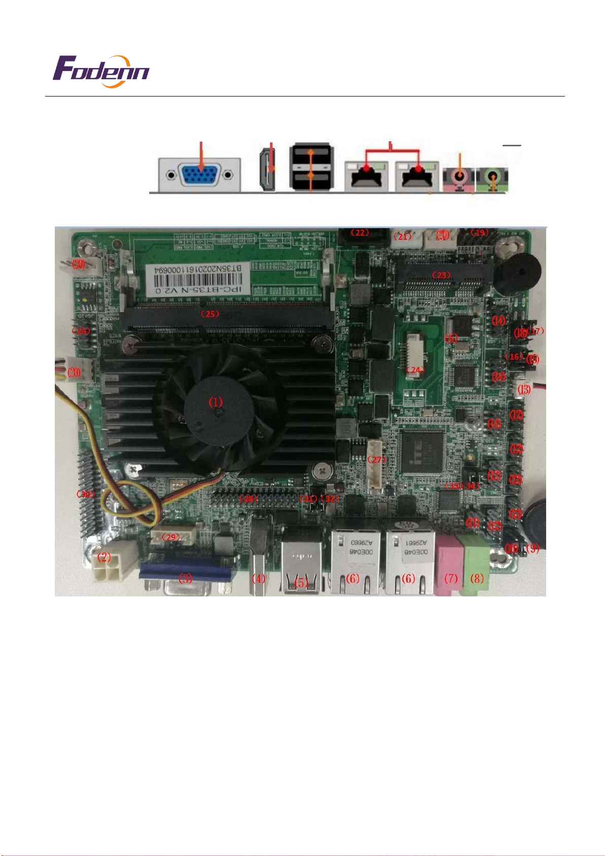
VGA Port
HDMI Port RJ-45 Port
USB 2.0 Port
MIC-IN
LINE-OUT
2.1
Port Explanatory Chart
1. CPU 2. Power Socket 3. VGA 4. HDMI
5. USB2.0 6.RJ45 7.MIC 8. Line-Out
9. JC21 10.JC61 11. Power Amilifier Pin 12.Series Pin
13. Battery Pin 14.F-USB 1/2/3 15.CLR-CMOS1 16.J1-485
17.J1-485 18.J1-422 19.F-Panel 20.System Fan,CPU Fan Pin
21.SATA Power 22.SATA 23.Mini-PCIE Slot 24. SIM Slot
25.Memory Slot 26.JGPIO 27. JPS2 28.LVDS Pin
29.Invert Pin 30.EDP Pin 31. LVDS-PWR2 32.LVDS-PWR1
33.JC11 34.JC12
4 / 9
Fodenn Electronic Technology Co.,Ltd
Add: 3rd floor, Building B, Runchang industrial park, Zhonghao 2 road,
Bantian street, Longgang district, Shenzhen
Tel:0755-86329789 Fax:0755-83689236 Email:oversea1@fodenn.com
2.2
Inside Port
2.2.1
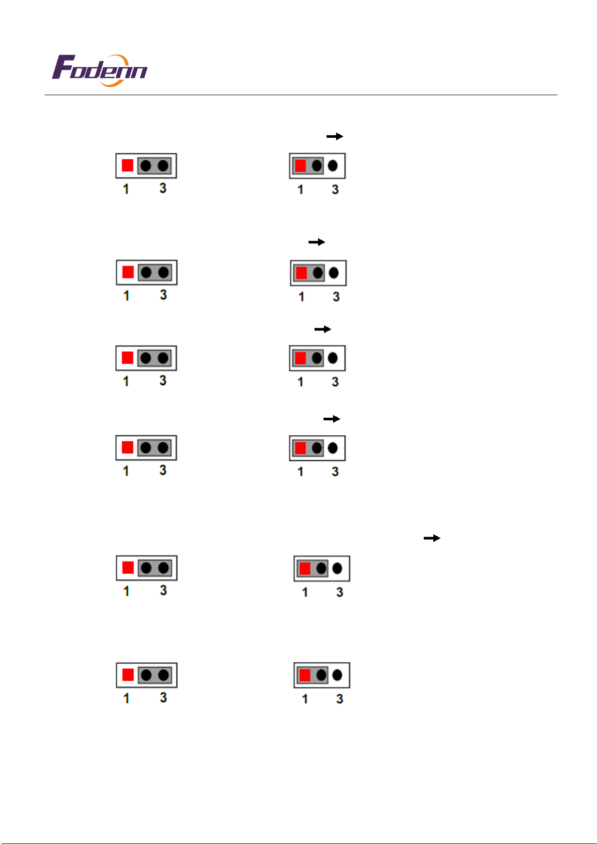
JC11(3-PIN):COM1Portfunctionsetup(9-PIN)
JC11
COM1
PIN2-3Connection:RS232 PIN1-2Connection:RS232(PIN1is+5V)
JC12(3-PIN):COM1Port function settings (9-PIN)
JC12
COM1
PIN2-3Connection:RS232 PIN1-2Connection:RS232(PIN5is+12V)
JC21(3-PIN):COM2Port function settings(9-PIN)
JC21
COM2
PIN2-3Connection:RS232 PIN1-2Connection:RS232(PIN1is+5V) JC61(3-
PIN):COM1Port function settings(9-PIN)
JC61
COM6
PIN2-3Connection:RS232 PIN1-2 Connection:RS232(PIN1is+5V)
2.2.2 J1_485/J2_485(3-PIN):COM2
Port function settings(9-PIN)
J1_485/J2_485
COM2
PIN2-3 Connection:RS232 PIN1-2 Connection:
RS485 J1_422(3-PIN):COM2Port function settings(9-PIN)J1_422 COM2
PIN2-3Connection:RS232 PIN1-2Connection:RS422

5 / 9
Fodenn Electronic Technology Co.,Ltd
Add: 3rd floor, Building B, Runchang industrial park, Zhonghao 2 road,
Bantian street, Longgang district, Shenzhen
Tel:0755-86329789 Fax:0755-83689236 Email:oversea1@fodenn.com
3
2
2.2.3 COM1/2/3/4/5/6: Parameter definition
2
COM1/COM2(9 PIN)
2.2.4 F_USB1,F_USB2andF_USB3(9-PIN): Parameter definition, and optional USB2 (2.0mm) Pin
definition.F_USB1/2/3
2.2.5 J_485/422(4-PIN):RS485/RS422 Parameter definition
2TX485_422+ 2RX422+
2TX485_422- 2RX422-
2 4
2.2
,6 CLR_CMOS(3-PIN)
Note: CLR_CMOS allows you to clear the data in CMOS, including system setting data, such as system
password, date, time and system setting parameters. In order to clear and reset the system parameters to the
default settings, please turn off the computer and unplug the power cord, then use a jumper cap to short-
circuit pin2 and pin3 on CLR_CMOS for five seconds. If you need to clear the CMOS when completing the
BIOS refresh, you must first start the system, and then shut down the system before you perform the CMOS
clear operation.
PIN2-3: Clear COMS PIN1-2: Meaningless
2

6 / 9
Fodenn Electronic Technology Co.,Ltd
Add: 3rd floor, Building B, Runchang industrial park, Zhonghao 2 road,
Bantian street, Longgang district, Shenzhen
Tel:0755-86329789 Fax:0755-83689236 Email:oversea1@fodenn.com
2
2.3
2.3 Display output
The motherboard display output of this specification has four different signal output modes. The four signal
outputs can be arbitrarily selected in two groups for combination, whether it is synchronous dual display or
asynchronous dual display, which can be satisfied, respectively: VGA, HDMI, LVDS, EDP Four signal display
output
2.3.1
LVDS Displayoutput(30-PIN):parameterdefinition
29 30
2.3.2
LVDS_PWR1(3-PIN):LVDS ((VCC+3V/+5V power control)
LVDS_PWR1
LVDS
PIN2-3 Connection:VCC is+3.3V PIN1-2 Connection:VCC is+5V
LVDS_PWR2(3-PIN):LVDS(VCC+12V power control)
LVDS_PWR2
LVDS
PIN2-3 Connection::VCC is+12V PIN1-2Connection::Meaningless
Note: When LVDS_PWR2 is designed to be 12V, you need to remove the jumper cap on LVDS_PWR1
PIN
Definition
PIN
Definition
1
VCC
16
ACLK+
2
VCC
17
ADO3-
3
VCC
18
ADO3+
4
GND
19
BDO0-
5
GND
20
BDO0+
6
GND
21
BDO1-
7
ADO0-
22
BDO1+
8
ADO0+
23
BDO2-
9
ADO1-
24
BDO2+
10
ADO1+
25
GND
11
ADO2-
26
GND
12
AD02+
27
BCLK-
13
GND
28
BCLK+
14
GND
29
BDO3-
15
ACLK-
30
BDO3+
7 / 9
Fodenn Electronic Technology Co.,Ltd
Add: 3rd floor, Building B, Runchang industrial park, Zhonghao 2 road,
Bantian street, Longgang district, Shenzhen
Tel:0755-86329789 Fax:0755-83689236 Email:oversea1@fodenn.com
2
PIN
Definition
1
+12V
2
+12V
3
BACKLIGHT_ADJ
4
PWM
5
GND
6
GND
6
PIN 1
3
2.3.3
INVERT(6-PIN):LVDS invert Parameterdefinition
2.3.4
EDP Displayoutput(30-PIN):parameterdefinition
29 30
2.4
2.4 Built-in function interface of the board
2.4.1
F_AUDIO(4-PIN):AmplifierPINdefinition
2 4
PIN
Definition
PIN
Definition
1
VCC
16
TX3+
2
VCC
17
GND
3
VCC
18
GND
4
DET
19
AUX-
5
GND
20
HPD
6
GND
21
AUX+
7
TX0-
22
GND
8
TX1-
23
GND
9
TX0+
24
GND
10
TX1+
25
12V
11
GND
26
12V
12
GND
27
BKON
13
TX2-
28
5V
14
TX3-
29
BKCTL
15
TX2+
30
GND
PIN
Definition
1
LLINE2-R+
2
LLINE2-R-
3
LLINE2-L+
4
LLINE2-L-

8 / 9
Fodenn Electronic Technology Co.,Ltd
Add: 3rd floor, Building B, Runchang industrial park, Zhonghao 2 road,
Bantian street, Longgang district, Shenzhen
Tel:0755-86329789 Fax:0755-83689236 Email:oversea1@fodenn.com
PIN
Definition
1
KB_DATA
2
KB_CLK
3
GND
4
MS_DATA
5
MS_CLK
6
GND
7
+5V
PIN
Definition
1
GPIO
2
GPIO
3
GPIO
4
GPIO
5
GPIO
6
GPIO
7
GPIO
8
GPIO
9
+12V
10
GND
PIN
Sort
1
HDD_LED+
2
PWR_LED+
3
HDD_LED-
4
PWR_LED-
5
RESETSW
6
PWR_SW
7
GND
8
GND
9
NULL
10
GND
7
PIN 1
2
2.4.2
JPS2(7-PIN): Keyboard/Mouse PIN definition
2.4.3
JGPIO(10-PIN): GPIOParameterdefinition
9 10
2.4.4
F_PANEL(9-PIN): Host switch controller
9 / 9
Fodenn Electronic Technology Co.,Ltd
Add: 3rd floor, Building B, Runchang industrial park, Zhonghao 2 road,
Bantian street, Longgang district, Shenzhen
Tel:0755-86329789 Fax:0755-83689236 Email:oversea1@fodenn.com
PIN
Definition
1
GND
2
TXP
3
TXN
4
GND
5
RXN
6
RXP
7
GND
2.4.5
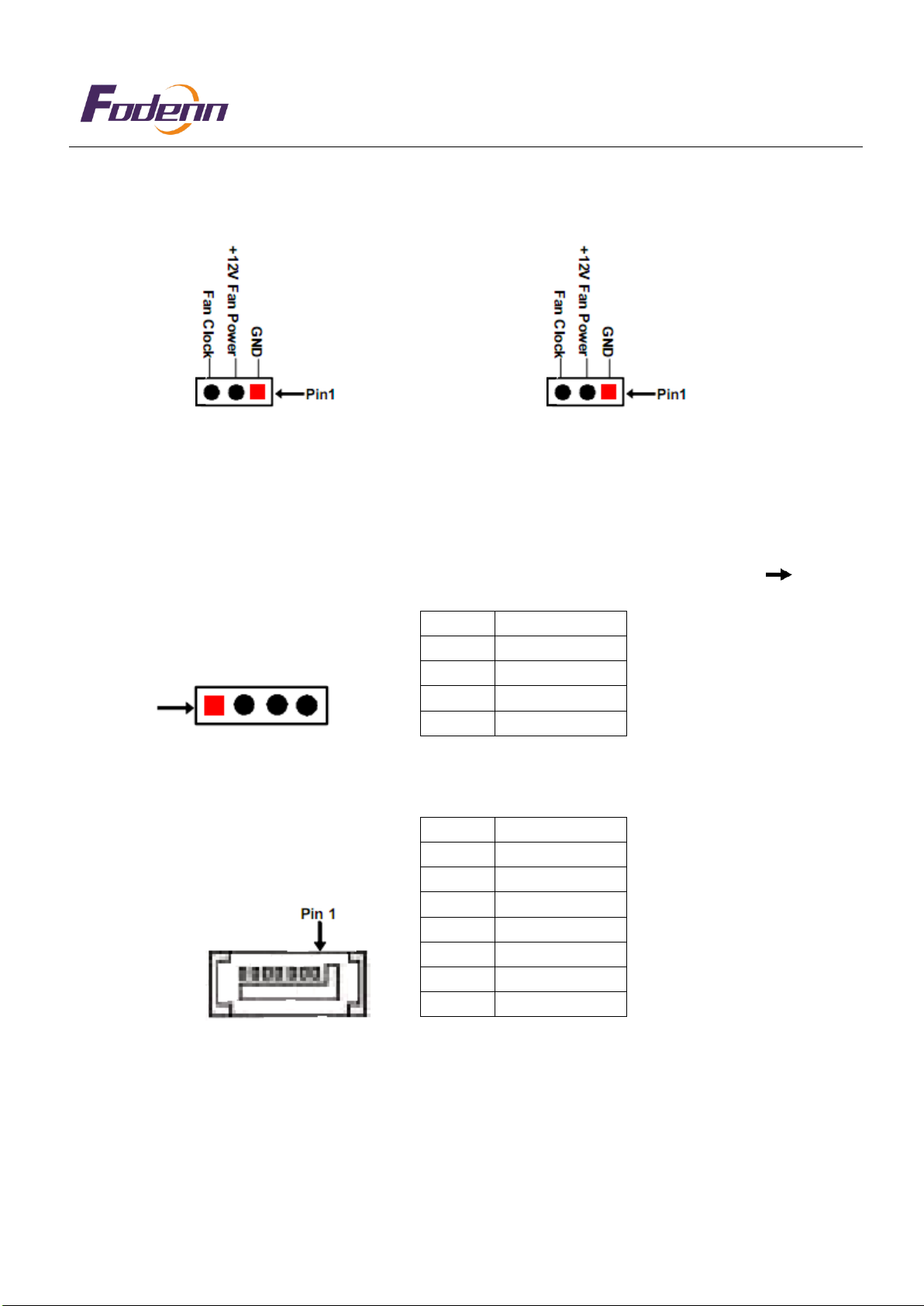
SYS_FAN/CPU_FAN(3-PIN): System fan/CPU fan
SYS_FAN CPU_FAN
2.5
System storage tool interface
The motherboard of this specification has three memory pair interfaces, two of which are standard MINI_PCIE
26-PIN (one on the front of the board and one on the back of the board), and a standard SATA 2 pair of
interfaces. In order to facilitate the application of SSD solid state drives and general hard drives. In addition, this
board has a SIM card slot that can support 3G module functions.
2.6.1 IDE_PWR(4-PIN): Common hard disk power access interface(SATA1)
IDE_PWR
SATA1
PIN 1 4
2.5.2 SATA1(7-PIN): Common version hard disk signal interface
Thank you for your understanding!
PIN
Definition
1
+5V
2
GND
3
GND
4
+12V
Table of contents
Other Fodenn Motherboard manuals


