DTK PAM-0079V User manual

PAM-0079V
High Performance
Pentium PCI Mainboard
User’s Guide
Edition 1.10
©1999 DTK Computer, Inc.
P/N: 155100-8797

I
WARNING
For the system to operate normally, please make sure JP1 of the mainboard is set as below. Refer
to Fig. 4 in this manual for the location JP1.
If JP1 is shorted to 2-3, no CMOS data can be retained.
CAUTION
The motherboard is an electrostatic sensitive device. Don’t open or handle except at a static-
free workstation.
POWER OFF
It needs to hold the power switch 4 seconds to turn off the power.
Windows, MS-DOS, and MS Word are trademarks of Microsoft Corporation.
Novell, Netware are trademarks of Novell, Inc.
Lotus, 1-2-3, and Symphony are trademarks of Lotus Development Corporation.
PC, AT, PC-DOS, OS/2 and Presentation Manager are trademarks of IBM Corporation.
UNIX is the trademark of AT&T.
Intel i82440EX and Pentium II are registered trademark of Intel Corporation.
All other brand and product names are trademarks or registered trademarks of their respective
companies.
The information presented in this publication has been carefully checked for reliability; however,
no responsibility is assumed for inaccuracies, whereas, specification is subjected to change
without notice.
1 2 3
JP1

II
CONTENTS
CHAPTER 1 INTRODUCTION 1
CHAPTER 2 JUMPER SETTINGS 5
2.1 JUMPERS PRESENTATION 5
2.2 CPU TYPE 5
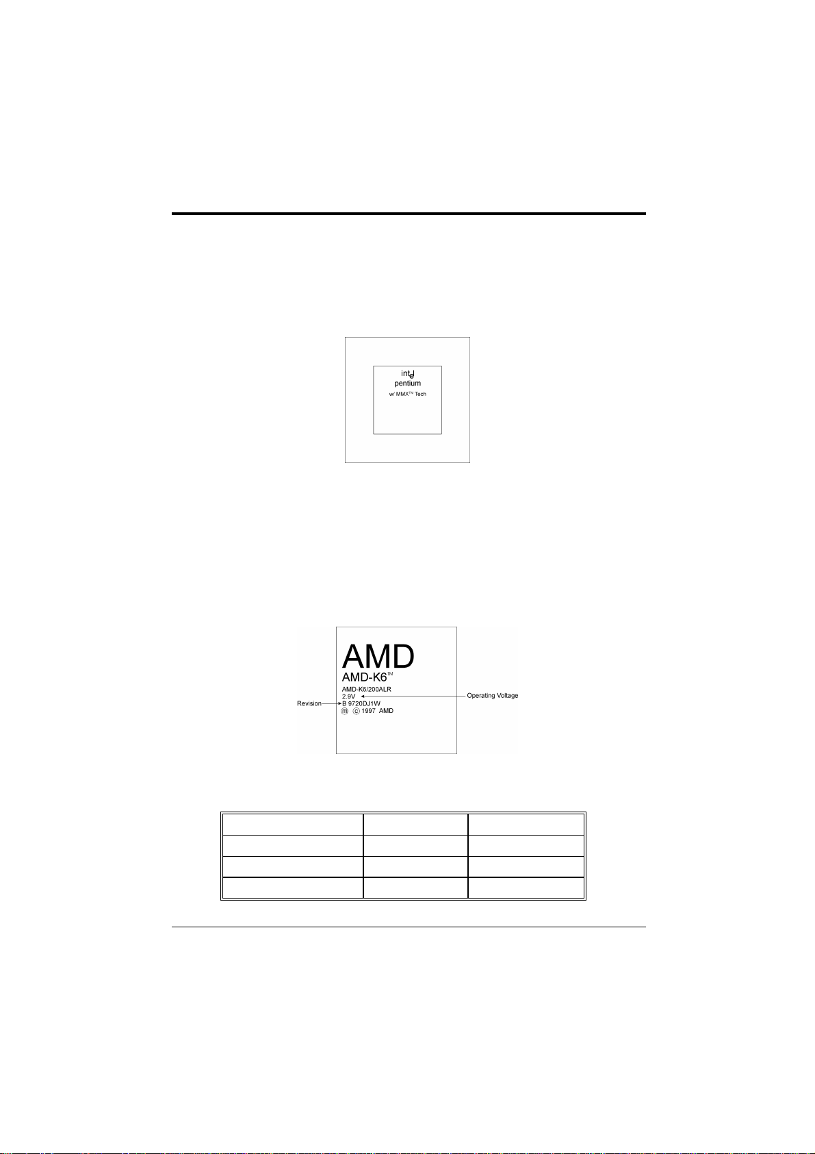
2.2.1 INTEL PENTIUM CPU 5
2.2.2 INTEL PENTIUM w/ MMXTECH (P55C) CPU 6
2.2.3 AMD-K6 CPU 6
2.2.4 AMD-K5 CPU 7
2.2.5 CYRIX 6x86 CPU 7
2.2.6 CYRIX 6x86L CPU 8
2.2.7 CYRIX 6x86MX CPU 8
2.2.8 IDT WinCHIP C6 CPU 9
2.3 GRAPHICAL DESCRIPTION OF JUMPER SETTINGS 10
2.4 CPU VOLTAGE 11
2.5 CPU EXTERNAL (BUS) FREQUENCY AND AGP FREQUENCY
SELECTION (SW1-4,5,6) 12
2.6 CPU TO BUS FREQUENCY RATIO (SW1-1,2,3) 12
2.7 SDRAM FREQUENCY SELECTION (SW1-7) 12
2.8 CPU SPEED 13
2.9 JP1 - CLEAR CMOS DATA 14
2.10 J6 – VOLTAGE SELECTION FOR SYSTEM ROM 14
2.11 JP7 – ONBOARD AUDIO SELECT 14
2.12 MEMORY CONFIGUARTION 15
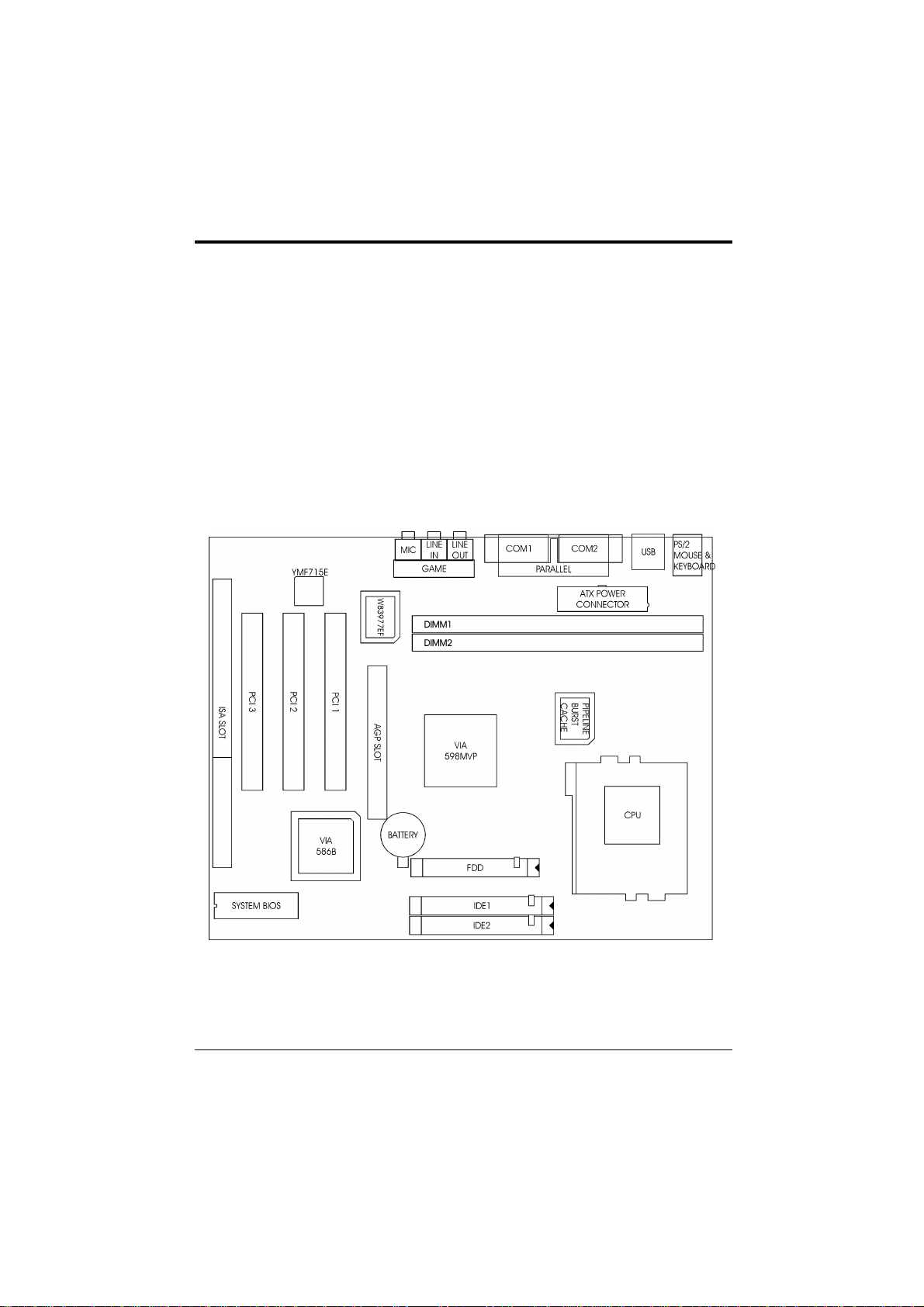
CHAPTER 3 CONNECTOR CONFIGURATION 17
3.1 J1 - POWER ON/OFF SWITCH 18
3.2 J3 – KEYLOCK CONNECTOR 18
3.3 J4 - SPEAKER 18
3.4 J5 - RESET 18
3.5 J7 – GREEN LED 19
3.6 J8 - HDD LED 19
3.7 JP2 - IrDA CONNECTOR 19
3.8 JP3 – WAKE UP ON LAN 20
3.9 JP4 – INTERNAL MODEM RING UP 20
3.10 SJ4 – CD-ROM AUDIO CONNECTOR (MITSUMI/PANASONIC) 20
3.11 SJ6 – CD-ROM AUDIO CONNECTOR (SONY) 20
3.12 CN5 - ATX POWER SUPPLY CONNECTOR 21
3.13 FAN1 – CPU FAN CONNECTOR 21
3.14 IDE0, IDE1 – PRIMARY/SECONDARY IDE CONNECTORS 21
3.15 FLOPPY - FLOPPY DRIVE CONTROLLER 21
3.16 PS/2 KEYBOARD CONNECTOR 22
3.17 PS/2 MOUSE CONNECTOR 22
3.18 UNIVERSAL SERIAL BUS PORT 0 & 1 22

III
3.19 SERIAL PORT COM1 & COM2 22
3.20 PARALLEL PORT CONNECTOR 22
3.21 AUDIO PORT CONNECTOR 22
CHAPTER 4 AWARD BIOS SETUP GUIDE 23
4.1 AWARD BIOS SETUP 23
4.2 STANDARD CMOS SETUP 25
4.3 BIOS FEATURES SETUP 26
4.4 CHIPSET FEATURES SETUP 28
4.5 POWER MANAGEMENT SETUP MENU 30
4.6 PCI CONFIGURATION 32
4.7 INTEGRATED PERIPHERALS SETUP MENU 34
4.8 LOAD SETUP DEFAULTS MENU 36
4.9 SUPERVISOR PASSWORD 36
4.10 USER PASSWORD 37
4.11 IDE HDD AUTO DETECTION 37
4.12 SCSI HARD DISK INSTALLATION 37
4.13 SAVE & EXIT SETUP MENU 37
4.14 EXIT WITHOUT SAVING MENU 38
CHAPTER 5 SOFTWARE INSTALLATION 39
5.1 VIA BUS MASTER PCI IDE DRVIVER FOR WINDOWS 95 39
5.2 AGP VxD SETUP PROGRAM39
5.3 VIA PCI MINIPORT DRIVER SETUP PROGRAM 40
5.4 VIA POWER MANAGEMENT CONTROLLER SETUP PROGRAM 40
5.5 SOUND DRIVER INSTALLATION 40
5.6 THE YSTATION APPLICATION FOR WINDOWS 95/WINDOWS 98 41
CHAPTER 6 FLASH AND DMI UTILITY 43
6.1 AWARD FLASH UTILITY 43
6.2 DESKTOP MANAGEMENT INTERFACE (DMI) OVERVIEW 45
APPENDIX A QUICK GUIDE 49

1
CHAPTER 1 INTRODUCTION
Preface
The motherboard is a 4 layer, Micro ATX form factor high performance PCI/AGP mainboard.
It includes VIA MVP3 system chipset, Winbond W83977EF Super I/O controller, Yamaha
YMF715E Sound Chip.
Features
Processor
•Intel Pentium/MMX, Cyrix 6x86/6x86L/6x86MX/M II, AMD K5/K6/K6-2/K6-III and IDT
C6 CPU
•The mainboard can run with following speeds:
90 ~450MHz
Chipset
•VIA VT82C598MVP (PCI/AGP System Controller)
•VIA VT82C586B (PCI Integrated Peripheral Controller)
•Winbond W83977EF (Super I/O Controller)
•Yamaha YMF715E (Audio Drive Sound Controller)
Main Memory
•Memory configurations up to 256MB SDRAM/EDO.
•DIMM socket for SDRAM (3.3V unbuffered).
•Support both Synchronous DRAM and Extended Data Output (EDO) Mode DRAM
Modules.
Multi I/O
•On board Multi-I/O supports two serial, one parallel ports and floppy drive controller.
•Serial ports are 16550 Fast UART compatible.
•Parallel port has EPP and ECP capabilities.
•PS/2 keyboard and PS/2 mouse connector is provided.
•IrDA supported.
•USB supported.
Accelerated Graphics Port (AGP) Interface
•A.G.P. specification compliant
•A.G.P. 66/133MHz devices supported
PCI IDE
•On board supports PCI Master IDE Controller, two connectors support up to four IDE
devices such as HDD, CD ROM drive and Tape Back-up drives, etc.
•PCI Master IDE controller supports PIO Mode 3 and 4 devices, I/O data transfer rate can be
up to 16.6MB/s.
•Ultra DMA Mode supported. Transfer rate can be up to 33MB/s.

Chapter 1
2
Sound Controller (Optional)
•Compatible with all major PC sound standards, including Sound BlasterPro, MPU-401
and Windows Sound System.
•Plug-and-Play support for Audio, Joystick, FM Controller, MPU-401.
•Wave Audio support sample rates from 4KHz to 44KHz.
•Full-duplex monophonic mode, half-duplex stereo mode.
System BIOS
•Award BIOS (128KB Flash EPROM).
Slots
•One AGP slot
•Three PCI slots
•One ISA slots
Form Factor
•Micro ATX Form Factor Size (244mm x 195mm) 4 Layer
Fig. 1 Key Components of the Mainboard

Introduction
3
Environment
Working Specifications
Actual Field MTBF (hours) 104,515 hours
Preventive Maintenance Not Required
Environmental Limits Operating Non-operating
Temperature 0 to 50 degree Celsius -10 to 65 Degree Celsius
Relative Humidity
(without condensation) 8 to 85% 5 to 95%
Altitude 10,000ft 40,000ft
Vibration 1,000Hz
Electricity 4.75 ∼5.25V
Power Specification
Configuration: 133MHz Intel P54C CPU, 32MB 60ns EDO DIMM, 512KB Cache, 3.5 inch
floppy drive, 840MB Hard Disk, running at DOS prompt.
DC Voltage Tolerance Consumption (mA)
+5V +/- 5% 860
+5V Standby +/- 5% 0.5
+5V +/- 5% 0
+12V +/- 5% 200
-12V +/- 5% 30

Chapter 1
4

5
CHAPTER 2 JUMPER SETTINGS
2.1 JUMPERS PRESENTATION
Pins 1 and 2 are shorted with a jumper cap.
1 2 3
Pins 2 and 3 are shorted with a jumper cap.
1 2 3
The jumper is shorted when the jumper cap is placed
over the two pins of the jumper.
The jumper is open when the jumper cap is removed
from jumper.
2.2 CPU TYPE
2.2.1 INTEL PENTIUM CPU
The pentium processors have different operation voltage. In order to using the CPU
Voltage correctly, the following is the marking for identify the CPU type.
Fig. 2a CPU Description
(Bottom Side)
Description :
X = Voltage Specification (S or V) Y = Timing Specification (S or M)
S = Standard Voltage (3.4V) S = Standard EDS timings
V = VRE 3.4 - 3.6V (3.5V) M = Min Valid Delay Spec.
Z = Dual Processing Support ( S or U)
S = Support DP/MP/UP
U = Not tested to support DP

Chapter 2
6
2.2.2 INTEL PENTIUM w/ MMX TECH (P55C) CPU
The Intel Pentium w/ MMXTech (P55C) CPU is offered with dual voltage supply
- 2.8V for core and 3.3V (I/O) interface. The following is the marking for identify
the CPU type. (The following diagram is provided as an example only. It does not
necessarily indicate a valid product marking.)
Fig. 2b CPU Description
(Top Side)
2.2.3 AMD-K6 CPU
The AMD-K6 CPU family requires dual voltage power for operation. The AMD-
K6/166, 200 require a voltage of 2.9V core and 3.3V I/O. The AMD-K6/233
requires a voltage of 3.2V core and 3.3V I/O. (The following diagram is provided as
an example only. It does not necessarily indicate a valid product marking.)
Fig. 2c CPU Description
(Top Side)
Operating Voltage I/O Voltage Core Voltage
2.2V 3.3V 2.2V
2.9V 3.3V 2.9V
3.2V 3.3V 3.2V

Jumper Settings
7
2.2.4 AMD-K5 CPU
The AMD-K5 family CPU operates on different operation voltage depending on the
CPU type. The operating voltage can be known through the marking on the surface of
the CPU. (The following diagram is provided as an example only. It does not
necessarily indicate a valid product marking.)
Fig. 2d CPU Description
(Top Side)
2.2.5 CYRIX 6x86 CPU
The Cyrix 6x86 has different nominal voltage depends on different lot. Please refer to
the CPU marking.
Fig. 2e CPU Description
(Top Side)
Marketing Recommended Nominal Voltage
3.3V or 3.52V 3.52V
028 3.52V
016 3.3V
Blank 3.52V

Chapter 2
8
2.2.6 CYRIX 6x86L CPU
The Cyrix 6x86L has different I/O and core voltage. Please refer to the CPU
marking.
Fig. 2f CPU Description
(Top Side)
2.2.7 CYRIX 6x86MX CPU
The Cyrix 6x86MX has different I/O and Core Voltage. Please refer to the CPU
marking.
Fig. 2g CPU Description
(Top Side)
I/O Voltage Core Voltage
Cyrix 6x86MX 3.3V 2.9V
Cyrix 6x86L 3.3V 2.8V

Jumper Settings
9
2.2.8 IDT WinCHIP C6 CPU
The IDT WinChip C6 CPU has different operating voltage. Please refer to the CPU
marking to identify the operating voltage.
Fig. 2h CPU Description

Chapter 2
10
2.3 GRAPHICAL DESCRIPTION OF JUMPER
SETTINGS
Fig. 3 Jumper Location of the mainboard

Jumper Settings
11
2.4 CPU VOLTAGE
(A) BIOS Setup
BIOS Auto detect or setup through BIOS. Different CPU requires different voltage.
Please refer the following table.
Auto BIOS Auto detect
2.2 2.2V AMD K6 and AMD-K6-2
2.4 AMD-K6-III; AMD-K6-2/450
2.8 Pentium MMX; Cyrix 6x86L
2.9 2.9V AMD K6; Cyrix 6x86MX/M II
3.2 3.2V AMD-K6/233
3.3 Intel Pentium, 3.3V IDT WinChip C6
3.52 Cyrix 6x86; AMD K5, 3.5V IDT WinChip C6
Table 1a
Note: If the BIOS doesn’t show “CPU Core Voltage” item in Chipset Features
Setup menu. You need setup the CPU Core Voltage by jumpers.
(B) Jumper Setup
The board also provides the hardware solution to select the CPU voltage.
Voltage Jumper Voltage Jumper
2.2V 3.2V
2.4V 3.3V
2.8V 3.5V
2.9V
Table 1b
JP10 JP9 JP8 JP10 JP9 JP8
JP10 JP9 JP8

Chapter 2
12
2.5 CPU EXTERNAL (BUS) FREQUENCY AND AGP
FREQUENCY SELECTION (SW1-4,5,6)
These switches tell the clock generator what frequency to send to the CPU and AGP.
The Bus clock times the Bus Ratio equals the CPU’s Internal frequency.
2.6 CPU TO BUS FREQUENCY RATIO (SW1-1,2,3)
These switches set the frequency ratio between the Internal frequency of the CPU
and the External frequency (called the Bus clock) within the CPU. These must be
set together with the above switches CPU External (Bus) Frequency Selection.
2.7 SDRAM FREQUENCY SELECTION (SW1-7)
This switch set the SDRAM frequency same as CPU External frequency or AGP
frequency.
SW1-7 : ON SDRAM frequency = AGP frequency
SW1-7 : OFF SDRAM frequency = CPU External frequency
ON
1 2 3 4 5 6 7

Jumper Settings
13
2.8 CPU SPEED
Bus Freq. Ratio Setting Bus Freq. Setting
CPU Type Freq. Ratio Freq. SW1-1 SW1-2 SW1-3 SW1-4 SW1-5 SW1-6
Intel Pentium 90MHz 1.5x 60MHz OFF OFF OFF ON ON ON
Intel Pentium 100MHz 1.5x 66MHz OFF OFF OFF OFF ON ON
Intel Pentium 120MHz 2.0x 60MHz ON OFF OFF ON ON ON
Intel Pentium 133MHz 2.0x 66MHz ON OFF OFF OFF ON ON
Intel Pentium 150MHz 2.5x 60MHz ON ON OFF ON ON ON
Intel Pentium 166MHz 2.5x 66MHz ON ON OFF OFF ON ON
Intel Pentium 200MHz 3.0x 66MHz OFF ON OFF OFF ON ON
Intel Pentium w/MMX 166MHz 2.5x 66MHz ON ON OFF OFF ON ON
Intel Pentium w/MMX 200MHz 3.0x 66MHz OFF ON OFF OFF ON ON
Intel Pentium w/MMX 233MHz 3.5x 66MHz OFF OFF OFF OFF ON ON
AMD-K5-PR120 120MHz 2.0x 60MHz ON OFF OFF ON ON ON
AMD-K5-PR133 133MHz 2.0x 66MHz ON OFF OFF OFF ON ON
AMD-K5-PR166 166MHz 2.5x 66MHz ON ON OFF OFF ON ON
AMD-K6/166 166MHz 2.5x 66MHz ON ON OFF OFF ON ON
AMD-K6/200 200MHz 3.0x 66MHz OFF ON OFF OFF ON ON
AMD-K6/233 233MHz 3.5x 66MHz OFF OFF OFF OFF ON ON
AMD-K6/266 266MHz 4.0x 66MHz ON OFF ON OFF ON ON
AMD-K6/300 300MHz 4.5x 66MHz ON ON ON OFF ON ON
AMD-K6-2/250 250MHz 2.5x 100MHz ON ON OFF OFF OFF OFF
AMD-K6-2/266 266MHz 4.0x 66MHz ON OFF ON OFF ON ON
AMD-K6-2/300 300MHz 3.0x 100MHz OFF ON OFF OFF OFF OFF
AMD-K6-2/333 333MHz 3.5x 95MHz OFF OFF OFF ON OFF OFF
AMD-K6-2/350 350MHz 3.5x 100MHz OFF OFF OFF OFF OFF OFF
AMD-K6-2/380 380MHz 4.0x 95MHz ON OFF ON ON OFF OFF
AMD-K6-2/400 400MHz 4.0x 100MHz ON OFF ON OFF OFF OFF
AMD-K6-2/450 450MHz 4.5x 100MHz ON ON ON OFF OFF OFF
AMD-K6-III/400 400MHz 4.0x 100MHz ON OFF ON OFF OFF OFF
AMD-K6-III/450 450MHz 4.5x 100MHz ON ON ON OFF OFF OFF
Cyrix 6x86L-PR150 120MHz 2.0x 60MHz ON OFF OFF ON ON ON
Cyrix 6x86L-PR166 133MHz 2.0x 66MHz ON OFF OFF OFF ON ON
Cyrix 6x86L-PR200 150MHz 2.0x 75MHz ON OFF OFF ON ON OFF
Cyrix 6x86MX-PR166 150MHz 2.5x 60MHz ON ON OFF ON ON ON
Cyrix 6x86MX-PR200 150MHz 2.0x 75MHz ON OFF OFF ON ON OFF
Cyrix 6x86MX-PR200 166MHz 2.5x 66MHz ON ON OFF OFF ON ON
Cyrix 6x86MX-PR233 188MHz 2.5x 75MHz ON ON OFF ON ON OFF
Cyrix 6x86MX-PR233 200MHz 3.0x 66MHz OFF ON OFF OFF ON ON
Cyrix M II-300 225MHz 3.0x 75MHz OFF ON OFF ON ON OFF
Cyrix M II-300 233MHz 3.5x 66MHz OFF OFF OFF OFF ON ON
Cyrix M II-333 250MHz 2.5x 100MHz ON ON OFF OFF OFF OFF
Cyrix M II-350 300MHz 3.0x 100MHz OFF ON OFF OFF OFF OFF
IDT WinChip C6-180 180MHz 3.0x 60MHz OFF ON OFF ON ON ON
IDT WinChip C6-200 200MHz 3.0x 66MHz OFF ON OFF OFF ON ON
IBM 6x86MX-PR266 208MHz 2.5x 83MHz ON ON OFF OFF ON OFF
Table 2

Chapter 2
14
2.9 JP1 - CLEAR CMOS DATA
JP1 is used to clear the content of the CMOS Data in the RTC (build in PIIX4 chip).
Table 3: Clear CMOS Data
2.10 J6 – VOLTAGE SELECTION FOR SYSTEM ROM
J6 is used to select the operation voltage of the System ROM.
Table 4: Voltage Selection for System ROM
2.11 JP7 – ONBOARD AUDIO SELECT
JP7 is set to select the Onboard Audio enabled or disabled.
Table 5: Onboard Audio Select

Jumper Settings
15
2.12 MEMORY CONFIGUARTION
The mainboard lets user upgrade system memory via DIMM sockets on the
mainboard. On board memory is located in four banks: Bank 0 - 3. Two DIMM
sockets are provided for EDO DRAM or Synchronous DRAM. Table 6 provides the
typical memory configurations supported by the mainboard.
The maximum memory size is up to 256MB (SDRAM/EDO). The size of each
DIMM can be 8MB, 16MB, 32MB, 64MB or 128MB.
Bank 0/1 (DIMM1) Bank 2/3 (DIMM2)
Installed None
None Installed
Installed Installed
Table 6

Chapter 2
16
Table of contents
Other DTK Motherboard manuals