FRONTGRADE GR716-BOARD User manual

Frontgrade Gaisler AB
Kungsgatan 12 | SE-411 19 Goteborg | Sweden
+46 31 7758650 | frontgrade.com/gaisler
2
GR716-BOARD
GR716-BOARD-UM
Oct 2023, Version 1.0
TABLE OF CONTENTS
1Introduction...................................................................................................................4
1.1 Scope and Purpose of the Document .....................................................................4
1.2 Reference Documents ............................................................................................4
2Abbreviations................................................................................................................4
3Introduction...................................................................................................................5
3.1 Overview.................................................................................................................5
3.2 Handling .................................................................................................................6
4Board Design................................................................................................................7
4.1 Board Block Diagram..............................................................................................7
4.2 Board Mechanical Configuration.............................................................................8
4.3 GR716 Microcontroller..........................................................................................11
4.4 Memory.................................................................................................................12
4.5 LVDS Interfaces....................................................................................................13
4.6 GPIO.....................................................................................................................14
4.7 Bootstrap Signals..................................................................................................14
4.8 Debug Support Unit Interfaces..............................................................................15
4.9 Oscillators and Clock Inputs .................................................................................16
4.10 Power Supply and Voltage Regulation..................................................................17
4.11 Reset Circuit and Button.......................................................................................20
4.12 Watchdog..............................................................................................................20
5Setting Up and Using the Board .................................................................................20
6Interfaces and Configuration.......................................................................................21
6.1 List of connectors..................................................................................................21
6.2 List of Oscillators, Switches and LED’s.................................................................23

Frontgrade Gaisler AB
Kungsgatan 12 | SE-411 19 Goteborg | Sweden
+46 31 7758650 | frontgrade.com/gaisler
3
GR716-BOARD
GR716-BOARD-UM
Oct 2023, Version 1.0
List of Figures
Figure 3-1 GR716-BOARD Development Board ...............................................................5
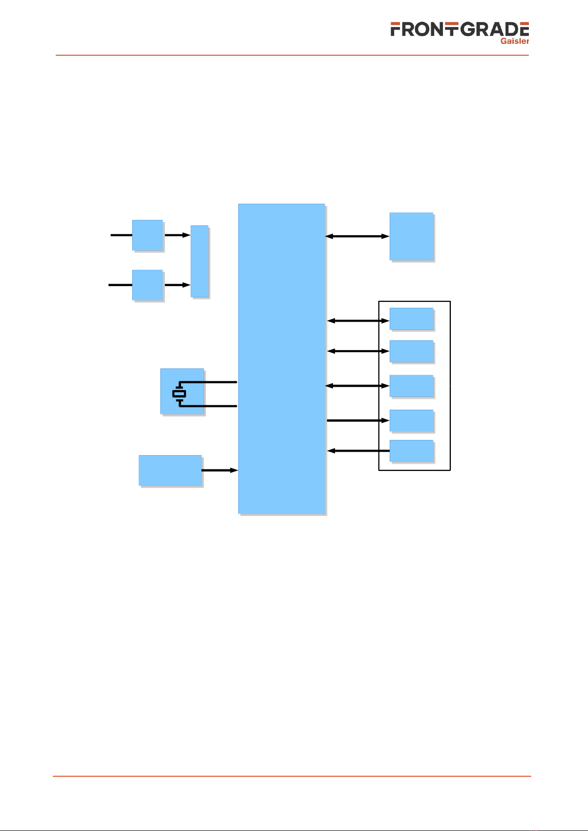
Figure 4-1 GR716-BOARD Board Block Diagram .............................................................7
Figure 4-2 GR616-BOARD Board Dimensions..................................................................8
Figure 4-3 GR716-BOARD mounted on a GR716-CPCI-DEV Carrier board ....................9
Figure 4-4 GR716-TEST-MEMORY BOARD...................................................................10
Figure 4-5 GR716-TEST-ADCDAC BOARD....................................................................10
Figure 4-6 GR716 Microcontroller Block Diagram ...........................................................11
Figure 4-7 GR716 Package.............................................................................................11
Figure 4-8 SPI Boot Memory Connectons.......................................................................12
Figure 4-9 Debug Support Unit connections....................................................................15
Figure 4-10 GR716-DSU-USB Adapter..........................................................................15
Figure 4-11 Board level Clock Distribution Scheme .......................................................16
Figure 4-12 Power Regulation Scheme .........................................................................18
Figure 4-13 Power Supply Configuration Jumpers.........................................................19
Figure 6-1 PCB Top View ................................................................................................24
Figure 6-2 PCB Bottom View...........................................................................................25
Figure 6-3 PCB Top View (Photo)....................................................................................26
Figure 6-4 PCB Bottom View (Photo) ..............................................................................27
List of Tables
Table 1: Bootstrap Resistor Settings..................................................................................14
Table 2: List of Connectors ................................................................................................21
Table 3: J1 Screw Terminal Connector for Input Voltages..................................................21
Table 4: J2 POWER-External Power Connector ................................................................21
Table 5: Expansion connector P1 Pin-out .........................................................................22
Table 6: Expansion connector P2 pin-out ..........................................................................22
Table 7: List and definition of Oscillators and Crystals.......................................................23
Table 8: List and definition of PCB mounted LED's............................................................23
Table 9: List and definition of Switches ..............................................................................23
Table 10: Definition of Switch S1 functions (refer to [RD1]) ...............................................23

Frontgrade Gaisler AB
Kungsgatan 12 | SE-411 19 Goteborg | Sweden
+46 31 7758650 | frontgrade.com/gaisler
4
GR716-BOARD
GR716-BOARD-UM
Oct 2023, Version 1.0
1 INTRODUCTION
1.1 Scope and Purpose of the Document
This document provides a User's Manual and Interface document for the “GR716-BOARD”
Development and Demonstration board.
The work has been performed by Frontgrade Gaisler AB, Göteborg, Sweden.
1.2 Reference Documents
[RD1] GR716, Data Sheet and User's Manual",Frontgrade Gaisler, GR716-UM-DS,
available from http://www.gaisler.com/index.php/products/components/GR716
[RD2] GR716-BOARD_schematic.pdf, Schematic
[RD3] GR716-BOARD_assy_drawing.pdf, Assembly Drawing
[RD4] GRMON3 User's Manual, available from:
https://www.gaisler.com/index.php/products/debug-tools/grmon3
2 ABBREVIATIONS
ASIC
Application Specific Integrated Circuit.
DSU
Debug Support Unit
EDAC
Error Detection and Correction
ESA
European Space Agency
ESD
Electro-Static Discharge
ESTEC
European Space Research and Technology Center
GPIO
General Purpose Input / Output
IC
Integrated Circuit
I/O
Input/Output
IP
Intellectual Property
LDO
Low Drop-Out
PCB
Printed Circuit Board
POL
Point of Load
SOC
System On a Chip
SPW
Spacewire
TBC
To Be Confirmed
TBD
To Be Defined

Frontgrade Gaisler AB
Kungsgatan 12 | SE-411 19 Goteborg | Sweden
+46 31 7758650 | frontgrade.com/gaisler
5
GR716-BOARD
GR716-BOARD-UM
Oct 2023, Version 1.0
3INTRODUCTION
3.1 Overview
This document describes the GR716-BOARD Development Board.
This equipment is intended to be used as a platform for the demonstration of the
Frontgrade Gaisler GR716 RAD Hard Microcontroller.
Furthermore, this board provides developers with a convenient hardware platform for the
evaluation and development of software for the GR716 microcontroller.
The GR716 Microcontroller features a fault-tolerant LEON3 SPARC V8 processor,
communication interfaces and on-chip ADC, DAC, Power-on-Reset, Oscillator, Brown-out
detection, LVDS transceivers, regulators to support for single 3.3V supply, ideally suited for
space and other high-rel applications.
The GR716 Microcontroller is a complex device with multifunctional pins whose function
depend on the mode of operation and programming of internal registers of the device. This
board treats the pins in a generic manner to allow easy access to all the pins and features
of the GR716 microcontroller.
Figure 3-1 GR716-BOARD Development Board

Frontgrade Gaisler AB
Kungsgatan 12 | SE-411 19 Goteborg | Sweden
+46 31 7758650 | frontgrade.com/gaisler
6
GR716-BOARD
GR716-BOARD-UM
Oct 2023, Version 1.0
The board contains the following main items as detailed in section 0 of this document:
•size 80 x 100mm
•two 2x32 pin stackable 0.1” headers allowing access to all I/O pins
•connector for single VIN power input (+5V to +12V)
•alternative connector for connections to individual device power supplies
•jumpers for power supply configuration
•on-board regulators converting from VIN to 3.3V & 1.8V
•256 Mbit SPI memory (Cypress, S25FL256SAGN in 8 pin WSON
package)
•socket for crystal (25MHz TBC)
•DIP switch for bootstrap settings
•on-board I2C voltage/current measurement
3.2 Handling
ATTENTION: OBSERVE PRECAUTIONS FOR
HANDLING ELECTROSTATIC SENSITIVE DEVICES
This unit contains sensitive electronic components which can be damaged by Electrostatic
Discharges (ESD). When handling or installing the unit observe appropriate precautions
and ESD safe practices.
When not in use, store the unit in an electrostatic protective container or bag.
When configuring the jumpers on the board, or connecting/disconnecting cables, ensure
that the unit is in an un-powered state.
When operating the board in a 'stand-alone' configuration, the power supply should be
current limited to prevent damage to the board or power supply in the event of an over-
current situation.
This board is intended for commercial use and evaluation in a standard laboratory
environment, nominally, 20°C. All devices are standard commercial types, intended for use
over the standard commercial operating temperature range (0 to 70ºC).

Frontgrade Gaisler AB
Kungsgatan 12 | SE-411 19 Goteborg | Sweden
+46 31 7758650 | frontgrade.com/gaisler
7
GR716-BOARD
GR716-BOARD-UM
Oct 2023, Version 1.0
4 BOARD DESIGN
4.1 Board Block Diagram
The GR716-BOARD Board provides the electrical functions and interfaces as represented
in the block diagram, Figure .Figure 4-2.
Figure 4-1 GR716-BOARD Board Block Diagram
Note that not all features and interfaces are available at the same time, and the
configuration of on-board resistors plus programming of registers is required to access
some of the features.
CRYSTAL
CRYSTAL
GR716
MICRO-
CONTROLLER
GR716
MICRO-
CONTROLLER
RESET_OUT
RESET_OUT
EXPANSION CONNECTOR
DCDC
DCDC SPI
FLASH
SPI
FLASH
GPIO
GPIO
DSU
DSU
BOOTSTRAP/
CONFIGURATION
BOOTSTRAP/
CONFIGURATION
3.3V
RESET_IN
RESET_IN
DCDC
DCDC
1.8V
VIN
VIN
LVDS
LVDS
CONFIGURATION
JUMPERS
CONFIGURATION
JUMPERS

Frontgrade Gaisler AB
Kungsgatan 12 | SE-411 19 Goteborg | Sweden
+46 31 7758650 | frontgrade.com/gaisler
8
GR716-BOARD
GR716-BOARD-UM
Oct 2023, Version 1.0
4.2 Board Mechanical Configuration
The board (80 x 100mm) and can be used 'stand-alone' on the bench-top simply an
external +5V power supply connected to connector J2. For mounting of the board on a
carrier or expansion board, four M2.5 mounting holes are provided in the corners of the
board, as shown in the figure below.
Figure 4-2 GR616-BOARD Board Dimensions
The expansion connectors P1 and P2 of the GR716-BOARD are stacking style connectors
having a socket on the bottom side and an extended pin on the top side. In a stand-alone
configuration the pins on the top side allow easy access for Logic Analyser or Oscilloscope
probing for all the functional microcontroller pins.
The sockets on the bottom side allow the board to be plugged on to a carrier board to
conveniently enable further development testing.
The CPCI format board providing GPIO, SPW, Serial (via FTDI-USB) and analog coaxial
connector which has been developed for this purpose is shown in Figure 4-3.

Frontgrade Gaisler AB
Kungsgatan 12 | SE-411 19 Goteborg | Sweden
+46 31 7758650 | frontgrade.com/gaisler
9
GR716-BOARD
GR716-BOARD-UM
Oct 2023, Version 1.0
Figure 4-3 GR716-BOARD mounted on a GR716-CPCI-DEV Carrier board
Alternatively, the stacking connector concept allows the interface functions to be expanded
by stacking the GR716-BOARD to other boards in a concept similar to PC104.
A test board for adding memory (SPI serial, 8 bit parallel FLASH and 8 bit SRAM) is shown
in Figure 4-4, and a test board for exercising the Analog features of the GR716
microcontroller is shown in Figure 4-5.
This concept also provides a convenient way for User Defined interface boards to be
developed and connected to the GR716-BOARD, if other functions or features are to be
demonstrated.

Frontgrade Gaisler AB
Kungsgatan 12 | SE-411 19 Goteborg | Sweden
+46 31 7758650 | frontgrade.com/gaisler
11
GR716-BOARD
GR716-BOARD-UM
Oct 2023, Version 1.0
4.3 GR716 Microcontroller
The Frontgrade Gaisler GR716 Microcontroller features a fault-tolerant LEON3 SPARC V8
processor, communication interfaces and on-chip ADC, DAC, Power-on-Reset, Oscillator,
Brown-out detection, LVDS transceivers, regulators to support for single 3.3V supply,
ideally suited for space and other high-rel applications.
Figure 4-6 GR716 Microcontroller Block Diagram
The GR716 Microcontroller is a complex device with many modes of operation. For the
details of the interfaces, operation and programming, refer to [RD1].
The GR716 microcontroller is packaged in a 132-pin, 0.635mm pitch Ceramic Quad Flat
Pack package (housing: 24 x 24 mm).
Figure 4-7 GR716 Package

Frontgrade Gaisler AB
Kungsgatan 12 | SE-411 19 Goteborg | Sweden
+46 31 7758650 | frontgrade.com/gaisler
12
GR716-BOARD
GR716-BOARD-UM
Oct 2023, Version 1.0
4.4 Memory
The memory configuration installed on the board comprises:
•256 Mbit SPI serial boot prom (Cypress, S25FL256SAGN)
The SPI boot memory is connected directly to the SPIM interface of the GR716 Micro-
controller. Although the SPI memory chip can operate in a x4 data mode, only a x1 data
mode is usable with the GR716.
Figure 4-8 SPI Boot Memory Connectons

Frontgrade Gaisler AB
Kungsgatan 12 | SE-411 19 Goteborg | Sweden
+46 31 7758650 | frontgrade.com/gaisler
13
GR716-BOARD
GR716-BOARD-UM
Oct 2023, Version 1.0
4.5 LVDS Interfaces
The GR716 microcontroller provides a set of three LVDS input pairs and three LVDS
output pairs which are configurable from software via configuration registers to provide
SpaceWire or SPI4SPACE interfaces.
These signals are connected from the GR716 microcontroller to the Expansion connector,
P2.
100 Ohm Termination resistors and fail-safe resistors for the LVDS receiver signals are
mounted on the board close to the receiver.
This equipment has SPW ports that use Low Voltage Differential
Signalling (LVDS) which has limited common mode voltage protection. To
avoid damage to the SPW interfaces due to common mode voltage the
following actions should be performed before the equipments that will be
connected by SpaceWire are powered on.
•Before connecting any SpaceWire cables, make sure that there is no
voltage difference between the different equipment grounds. E.g.,
measure the voltage between the different equipment grounds with a
voltmeter. The result should be close to 0 V.
•After the SpaceWire cables are connected, make sure that the
equipment grounds are low ohmic connected to each other. E.g.,
measure the resistance between the different equipment grounds with a
multimeter in resistance mode. The result should be less than 1 Ω.
This board is intended to be used together with a carrier board. See the user’s manual of
the carrier board for information about the connection and grounding of the SpaceWire
interface. Users using the board stand alone or design their own carrier board, must
ensure that equipments connected via SPW have grounds that are connected together.

Frontgrade Gaisler AB
Kungsgatan 12 | SE-411 19 Goteborg | Sweden
+46 31 7758650 | frontgrade.com/gaisler
14
GR716-BOARD
GR716-BOARD-UM
Oct 2023, Version 1.0
4.6 GPIO
All 64 GPIO pins are connected from the GR716 Microcontroller to the Expansion
connector.
These General purpose I/O pins are 3.3V LVCMOS voltage levels.
Note though that most pins have multiple functions and in certain configurations may have
different input/output voltage requirements (e.g. ADC and DAC signals). Care must be
taken to account for this.
No current limiting or overvoltage protection components are included on
the GPIO signals of the GR716-BOARD board. The signals are connected
directly from the microcontroller to the expansion connector. Care must
therefore be taken to ensure that any external circuitry connected does not
exceed the allowable voltage limits for the input/output pins.
4.7 Bootstrap Signals
A number of features of the GR716 microcontroller are required to be set at power-on of
the processor, by means of bootstrap pins. A number of GPIO and function pins are pre-
defined for this purpose, according the definition Table 22 of [RD1].
To define the desired setting, an 8 pole, Double-Throw DIP switch (S1), is provided on the
board to connect these signals to either a pull-up or a pull-down resistor, or to allow the pin
to float.
Table 1: Bootstrap Resistor Settings
Pin
Function
Default
GPIO0
Disable EDAC
Up
GPIO17
Bypass Internal Boot Prom
Down
GPIO62
Enable Memory Test
Down
GPIO63
Redundant Memory Available
Down
DSUTX
Copy ASW image/SPW default frequency
Down
SPIM_MOS
I
Remote Access/Boot from Memory
Down
SPIM_SCK
Boot Source 0
Down
SPIM-SEL
Boot Source 1
Down

Frontgrade Gaisler AB
Kungsgatan 12 | SE-411 19 Goteborg | Sweden
+46 31 7758650 | frontgrade.com/gaisler
15
GR716-BOARD
GR716-BOARD-UM
Oct 2023, Version 1.0
4.8 Debug Support Unit Interfaces
Program download and debugging to the processor is performed using the GRMON
Debug Monitor tool from Frontgrade Gaisler ([RD4]). The GR716 microcontroller provides
a UART based DSU interface for Debug and control of the processor by means of a host
terminal, as represented in Figure 4-9.
Four control signals from the Debug Support Unit interface to the processor are
implemented:
DSUTX Debug UART Transmit
DSURX Debug UART Receive
DSUEN This signal is pulled high on the board to enable
Debugging
DSUBRE This signal is pulled low on the board
To connect to a host computer, a small adapter can be used as shown in Figure 4-10.
Figure 4-9 Debug Support Unit connections
Figure 4-10 GR716-DSU-USB Adapter
GR716
DSUBRE→
HOST
TERMINAL/COMPUTER
USB
DSUEN→
FTDI
DSURX→
DSUTX←
EXPANSION
CONNECTOR
GR716-DSU-USB

Frontgrade Gaisler AB
Kungsgatan 12 | SE-411 19 Goteborg | Sweden
+46 31 7758650 | frontgrade.com/gaisler
16
GR716-BOARD
GR716-BOARD-UM
Oct 2023, Version 1.0
4.9 Oscillators and Clock Inputs
The oscillator and clock scheme for the GR716-BOARD Board is shown in Figure 4-11.
Two oscillator inputs are required: CLK for the main system clock, and SPW_CLK for the
SpaceWire clock of the microcontroller
To allow the GR716 Microcontroller to operate in a stand alone manner a crystal is
required on the board which is connected to the Crystal oscillator interface for the GR716.
On this board the crystal is mounted on a DIL8 socket adapter in order to allow various
crystal frequencies to be tested.
This generates an output clock, XO_OUT, which is connected to the CLK and SPW_CLK
inputs with jumpers.
In an alternative scenario, it may be preferred to have a separate CLK or SYS_CLK to
allow different frequencies to be used. In this case the jumpers can be moved and instead
an external 3.3V LVCMOS clock signal provided via the expansion connector.
For more details of the internal Crystal Oscillator, PLL structure and clock gating features
of the GR716, please refer to sections 9 and 10 of [RD1].
Figure 4-11 Board level Clock Distribution Scheme
GR716
microcontroller
SPW_CLK
CLK
XO_1
XTAL
25 MHz
Y1 XO_2
XO_OUT
EXPANSION
CONNECTOR

Frontgrade Gaisler AB
Kungsgatan 12 | SE-411 19 Goteborg | Sweden
+46 31 7758650 | frontgrade.com/gaisler
17
GR716-BOARD
GR716-BOARD-UM
Oct 2023, Version 1.0
4.10 Power Supply and Voltage Regulation
The power configuration is represented in Figure 4-12.
By means of configuration jumpers, several configurations can be tested:
1. Individual voltages from external bench supplies connected to the screw
terminal connector J1 to provide
+VADC (+3V3 nominal)
+VREF (+3V3 nominal)
+VDAC (+3V3 nominal)
+VLVDS (+3V3 nominal)
This allows individual power supplies to be tested over min/nom/max by
varying the supply voltages.
2. Single VIN (+12V nominal) input supply connector to J1.
3. Single VIN (+12V nominal) input supply connector to J2.
4. VIN provided from external circuitry connected to Expansion connector P2.
With reference to the setting of the jumpers shown in Figure 4-13:
•In case 1, jumpers JP1, JP2, JP3 and JP4 should be set to position 1-2.
•In cases 2,3,4 VIN is regulated with two LMZ21701 micro Point-of-Load regulators to
generate a regulated VDDIO (+3.3V) and VDD_CORE (+1.8V). In these cases,
jumpers JP1, JP2, JP3 and JP4 should be set to position 2-3.
•Jumper JP5 (VPLL) should not be installed. VPLL is provided from the 1V8 voltage
generated by the LDO regulator inside the GR716.
•If the GR716 is to be operated from a single 3.3V, and the internal LDO is to be used
to generate the VDDCORE voltage of 1.8V then JP6 should be installed and JP7
removed.
•If the GR716 is to be operated from both the POL generated 3.3V and 1.8V supplies,
then JP6 should be removed and JP7 installed. In this situation, the internal LDO is
disabled and VDDCORE voltage of 1.8V is provided form the POL regulator.
At the output of the 3.3V and 1.8V POL regulators, 20 mOhm sense resistors and INA219
Current/Power Monitor circuits with an I2C interface are incorporated on the board. The
I2C signals (SDA, SCL) are connected to the Expansion connector P2 to allow the
current/voltage to be measured using an I2C master circuit.

Frontgrade Gaisler AB
Kungsgatan 12 | SE-411 19 Goteborg | Sweden
+46 31 7758650 | frontgrade.com/gaisler
18
GR716-BOARD
GR716-BOARD-UM
Oct 2023, Version 1.0
Figure 4-12 Power Regulation Scheme
J2 +3V3
DCDC
GR716
5V min
12V nom
14.5V max LMZ21701
1A max
VDDA_ADC
VDDA_DAC
+3V3
VDDA_REF
VDDA_LVDS
VDD_LDO_IN
VDD_IO
VDD_CORE
FILTER
FILTER
FILTER
FLASH
EXPANSION
CONNECTOR
+1V8
+1V8
DCDC
J1
I2C measure
I2C measure
LMZ21701
1A max
+VIN
+VLVDS
+VREF
+VDAC
+VADC

Frontgrade Gaisler AB
Kungsgatan 12 | SE-411 19 Goteborg | Sweden
+46 31 7758650 | frontgrade.com/gaisler
20
GR716-BOARD
GR716-BOARD-UM
Oct 2023, Version 1.0
4.11 Reset Circuit and Button
The GR716 microcontroller includes an internal RESET circuit with Brown-out detector to
reset the processor and its peripherals (see section 8 of [RD1]).
The resulting low reset signal is present on the microcontroller pin RESET_OUT_N. This
signal is connected to the expansion connector, P2.
A manual reset of the microcontroller can be generated using the RESET_IN_N signal.
This signal is present on the expansion connector P2, and can be driven from an external
circuity if required. A miniature push button switch is provided on the GR716-DSU-USB
(Figure 4-10) to pull this signal low, when the button is pressed.
4.12 Watchdog
The GR716 microcontroller includes an internal Watchdog timer function which can be
used for the purpose of generating a system reset in the event of a software malfunction or
crash. Please refer to [RD1].
5 SETTING UP AND USING THE BOARD
The board is provided with a default configuration set by bootstrap settings.
For additional information, refer to [RD2] and for information about the Bootstrap signals,
refer to section 4.7.
To operate the board stand alone on the bench top, install the power configuration jumpers
appropriately, and +12V supply to the board connector J2.
ATTENTION! To prevent damage to board, please ensure that the
correct power supply voltage and polarity is used with the board.
Do not exceed +14.5V at the power supply input, as this may damage
the board.
The POWER_3V3 and POWER_1V8 power good LED’s should be
illuminated indicating that the power supply is present and the board is
generating the supply voltages that it requires.
Upon power on, using default bootstrap the processor will start executing instructions
beginning at the memory location 0x02000000, which is the start of the PROM. If the
PROM is 'empty' or no valid program is installed, the first executed instruction will be
invalid, and the processor will halt with an ERROR condition.
To perform program download and software debugging on the hardware it is necessary to
use the Frontgrade Gaisler GRMON3 debugging software, installed on a host PC (as
represented in Figure 4-9). Please refer to the GRMON3 documentation for the installation
of the software on the host PC (Linux or Windows), and for the installation of the
associated hardware dongle.
To perform software download and debugging on the processor, a link from the Host
computer to the DSU interface of the board is necessary. As described in section 0 this is
achieved via the FTDI USB interface.
Program download and debugging can be performed in the usual manner with GRMON3.
More information on the usage, commands and debugging features of GRMON3, is given
in the GRMON3 Users Manuals and associated documentation, [RD4].
Table of contents
Other FRONTGRADE Motherboard manuals