FUNAI SYLVANA 6413TB User manual

SERVICE MANUAL
THIS SERVICE MANUAL (6413TB/TVK131/W6413TB) CONTAINS ONLY DIFFERENCE
PARTS FROM ORIGINAL MODEL. FOR ALL OTHER DATA, SEE ORIGINAL SERVICE MAN-
UAL MODELS ST413B.
13"COLOR TELEVISION
6413TB/TVK131/W6413TB

IMPORTANT SAFETY NOTICE
Proper service and repair is important to the safe, reliable operation of all
Funai Equipment. The service procedures recommended by Funai and de-
scribed in this service manual are effective methods of performing service
operations. Some of these service special tools should be used when and
as recommended.
It is important to note that this service manual contains various CAUTIONS
and NOTICES which should be carefully read in order to minimize the risk of
personal injury to service personnel. The possibility exists that improper
service methods may damage the equipment. It also is important to under-
stand that these CAUTIONS and NOTICES ARE NOT EXHAUSTIVE. Funai
could not possibly know, evaluate and advice the service trade of all conceiv-
able ways in which service might be done or of the possible hazardous con-
sequences of each way. Consequently, Funai has not undertaken any such
broad evaluation. Accordingly, a servicer who uses a service procedure or
tool which is not recommended by Funai must first use all precautions thor-
oughly so that neither his safety nor the safe operation of the equipment will
be jeopardized by the service method selected.
TABLE OF CONTENTS
Block Diagrams..................................................................................................................................................... 1-1
Schematic Diagrams / CBA’ s and Test Points ..................................................................................................... 2-1
Parts List............................................................................................................................................................... 3-1

L1302BLIF
BLOCK DIAGRAMS
1-1 1-2
32
21
17
12
29
25
27
20
28
30
5
1
64
62
10
VCXO
INV
V.RAMP
REF
FILTER
VERTICAL
COUNT
DOWN
RGB
EXT.
INPUT
X331
3.58MHz
HORIZONTAL
COUNT
DOWN
ADJ
DET
VCC
ADJ
RGB MATRIX
CONTRAST BRIGHT CLAMP
CLAMP
DELAY
HV
BLK
WH301A TO WH301B
DRIVE
AMP
VIDEO
MUTE
VIDEO
TONE
BLACK
STRETCH
GAMMA
H
VCO
BGP
GENE.
KILLER
DET
CHROMA
BPF
V-SYNC
TRIG.
SYNC
SEPA
CHROMA
TRAP
VCO
ADJ 4.5MHz
TRAP
JK701
V-IN
FBP
H-DRIVE
ACL/ABL
CF301
4.5MHz
BPF
CF302
VIDEO
DET
VIF
AMP
SAW
FILTER
KEY
SWITCH
SF1
APC
DET
INTELLIGENT
MONITORING
ACC
DET
ACC
HPF
LPF
AFT
IC333 VIDEO/AUDIO/CHROMA/DEFLECTION/IF
VCO
LOCK DET
TUNER
LINE
CHROMA
APC DET
14
31
15
16
6
7
40
43
34
36
49
DEMODULATOR
AFC-2
AFC-1
H.COINCIDENCE
EQ
ELIMINATE
BUS
I/F
BUS
CONTROL
TUNER
LINE
X2
TU1
IF
AGC
TU
TP301
AGC
SDA
SCL
EXT.CLK
1
2
11
5
4
8
TP300
GND
IC101 TV MICON
IC151
MEMORY
SW101-
SW106
V-SYNC
H-SYNC
OSD-R
OSD-G
OSD-B
C-VIDEO
SD
KEY-IN
SDA
SCL
SDA
SCL
I2C-OPEN
V-DRIVE
V.RAMP NF
31
32
11
33
17
28
2
1
39
40
41
42
SDA 4
I2C-OPEN 2
INT.MONITOR
1
FM ANT.
1
SCL 5
CN301
CN101
(NO CONNECTION)
CN301 is used for
adjustment at factory
26
27
10
PROTECT-1
PROTECT-2
PROTECT1
PROTECT2
REMOCON
FROM/TO
CRT/H.V. BLOCK
OSD-BLK
5
6WF1
WF2
FROM/TO
CRT/H.V. BLOCK
TU AUDIO TO AUDIO/POWER
CONTROL BLOCK
TO
CRT/H.V. BLOCK
BLUE5
GREEN4
RED3
WF16
IF/Video/System Control Block Diagram
VIDEO SIGNALRF/IF SIGNAL AUDIO SIGNAL
REMOTE
SENSOR
RCV101
P-ON-H
P-ON-H
SDA
SCL
35
A-MUTE-H
A-MUTE-H 6
TO AUDIO/POWER
CONTROL
BLOCK
RESET25RESET
HPF
TRAP
SW
IF AGC
RF AGC
57
QIF
AGC
QIF
DET
FM
TV
TV
FM
61
(TO FM ANT.) W6413TB
W6413TB

Audio/Power Control Block Diagram
MAIN CBA
AUDIO SIGNAL
WF6
1-3 1-4
LIMITER FM DET AF
AMP
IC801
IC333
(AMP)
Q831
JK801
EARPHONE
JACK
LINE
TUNER
NOTE FOR WIRE CONNECTORS:
1. PREFIX SYMBOL "CN" MEANS CONNECTOR.
(CAN DISCONNECT AND RECONNECT.)
2. PREFIX SYMBOL "CL" MEANS WIRE-SOLDER HOLES OF THE PCB.
(WIRE IS SOLDERED DIRECTLY.)
TEST POINT INFORMATION
:INDICATES A TEST POINT WITH A JUMPER WIRE ACROSS A HOLE IN THE PCB.
:USED TO INDICATE A TEST POINT WITH A COMPONENT LEAD ON FOIL SIDE.
:USED TO INDICATE A TEST POINT WITH NO TEST PIN.
:USED TO INDICATE A TEST POINT WITH A TEST PIN.
SCL
SDA
5
10
52
47
13
55
46
33
39
42
41
A-IN
TU AUDIO
P-ON-H
BACK UP
BUS
I/F
ATT 50
POWER ON
CONTROL
+5.7V
REGULATOR
JK702
+5V CTRL
+5V CTRL2
+8V CTRL
BACKUP
CTRL
AUDIO
MUTE
A-MUTE-H
TO POWER SUPPLY
BLOCK
FROM/TO IF/VIDEO/
SYSTEM CONTROL
BLOCK
SP801
SPEAKER
CN801
7OUTPUT 1
FROM/TO IF/VIDEO
/SYSTEM CONTROL
BLOCK
FROM IF/VIDEO/
SYSTEM CONTROL
BLOCK
L1302BLA
P-ON-ON
P-ON-ON
RESET
RESET
BUS
CONTROL
VIDEO/AUDIO/CHROMA/DEFLECTION/IF
SP 1
SP-GND 1JS801
ST413B, F413TB

SCHEMATIC DIAGRAMS / CBA’S AND TEST POINTS
Standard Notes
Many electrical and mechanical parts in this chassis have special characteristics. These characteristics often pass
unnoticed and the protection afforded by them cannot necessarily be obtained by using replacement components
rated for higher voltage, wattage, etc. Replacement parts that have these special safety characteristics are identified
in this manual and its supplements; electrical components having such features are identified by the mark "
#
" inthe
schematic diagram and the parts list. Before replacing any of these components, read the parts list in this manual
carefully. The use of substitute replacement parts that do not have the same safety characteristics as specified in the
parts list may create shock, fire, or other hazards.
Note:
1.Do not use the part number shown on these drawings for ordering. The correct part number is shown in the parts
list, and may be slightly
different or amended since these drawings were prepared.
2.All resistance values are indicated in ohms (K=103, M=106).
3.Resistor wattages are 1/4W or 1/6W unless otherwise specified.
4.All capacitance values are indicated in µF (P=10−6µF).
5.All voltages are DC voltages unless otherwise specifi
Note of Capacitors:
ML --- Mylar Cap. PP --- Metalized Film Cap. SC --- Semiconductor Cap. L --- Low Leakage type
Temperature Characteristics of Capacitors are noted with the following:
B ---
±10% CH --- 0±60ppm/°C SL --- +350~-1000ppm/°C
Tolerance of Capacitors are noted with the following:
Z --- +80~-20%
Note of Resistors:
CEM --- Cement Res. MTL --- Metal Res. F --- Fuse Res.
(Top View) (Bottom View)
(Bottom View)
Electrolytic Capacitor
+
Transistor or Digital Transistor
NPN Transistor PNP Transistor
NPN Digital Transistor PNP Digital Transistor
(Top View)
(Top View)
E C B
E C B
Digital Transistor
CBA Symbols Schematic Diagram Symbols
E C B
(Top View)
(Top View)
E C B
E C B
Capacitors and transistors are represented by thefollowing symbols.
2-1 L1302SC

LILIST OF CAUTION, NOTES, AND SYMBOLS USED IN THE
SCHEMATIC DIAGRAMS ON THE FOLLOWING PAGES:
1. CAUTION: FOR CONTINUED PROTECTION AGAINST FIRE HAZARD, REPLACE ONLY WITH THE
SAME TYPE FUSE.ATTENTION: POUR UNE PROTECTION CONTINUE LES RISQES D’INCELE
N’UTILISER QUE DES FUSIBLE DE MEMO TYPE.
RISK OF FIRE-REPLACE FUSE AS MARKED.
2. CAUTION:
Fixed Voltage (or Auto voltage selectable) power supply circuit is used in this unit.
If Main Fuse (F001) is blown, first check to see that all components in the power supply circuit are not defective
before you connect the AC plug to the AC power supply. Otherwise it may cause some components in the power
supply circuit to fail.
3. Note:
(1)Do not use the part number shown on the drawings for ordering. The correct part number is shown in the parts
list, and may be slightly different or amended since the drawings were prepared.
(2)To maintain original function and reliability of repaired units, use only original replacement parts which are listed
with their part numbers in the parts list section of the service manual.
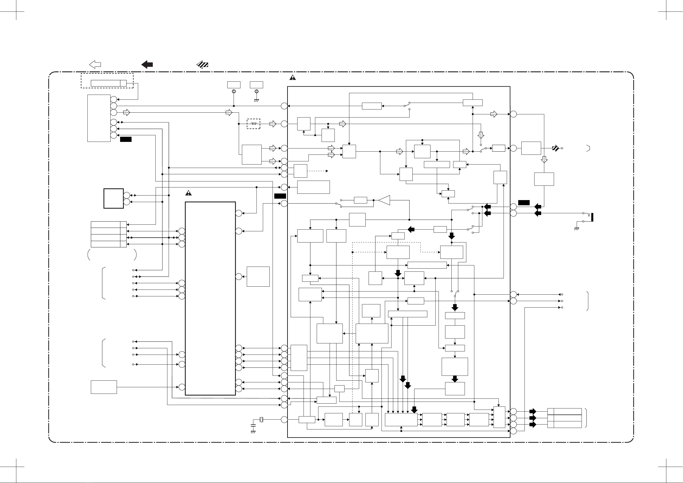
4. Wire Connectors
(1)Prefix symbol "CN" means "connector" (can disconnect and reconnect).
(2)Prefix symbol "CL" means "wire-solder holes of the PCB" (wire is soldered directly).
5. Note: Mark "•" is a leadless (chip) component.
6. Voltage indications on the schematics are as shown below:
7. How to read converged lines
1-D3
Distinction Area
Line Number
(1 to 3 digits)
Examples:
1. "1-D3" means that line number "1" goes to area "D3".
2. "1-B1" means that line number "1" goes to area "B1".
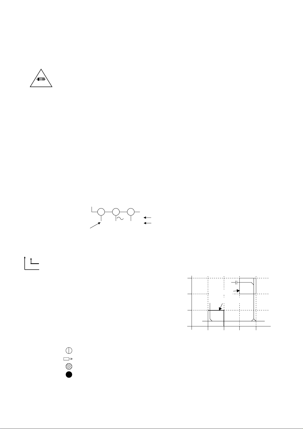
8. Test Point Information
2315.0
5.0
Voltage Indicates that the voltage
is not consistent here.
(3.0) (3.0) Power on mode
Power off mode
Unit: Volts
3
2
1
ABCD
1-B1
1-D3
AREA D3
AREA B1
: Indicates a test point with a jumper wire across a hole in the PCB.
: Used to indicate a test point with a component lead on foil side.
: Used to indicate a test point with no test pin.
: Used to indicate a test point with a test pin.
A V
2-2 L1302SC

2-3 L1302SCM1
Main 1/2 Schematic Diagram
2-4 2-5
MAIN 1/2
Ref No. Position
IC101 B-4
IC151 A-5
IC333 D-3
IC801 F-2
Q111 C-3
Q831 F-2
TP300 B-1
TP301 B-2
CN301 G-5
CN801 G-2
ICS
TRANSISTORS
TEST POINTS
CONNECTORS

A1
A2
A3
A4
A5
B1
B2
B3
B4
B5
C1
C2
C3
C4
C5
D1
D2
D3
D4
D5
E1
E2
E3
E4
E5
F1
F2
F3
F4
F5
G1
G2
G3
G4
G5

IF SIGNAL
VIDEO SIGNAL
AUDIO SIGNAL

Main 2/2 & CRT Schematic Diagram
2-6 L1300SCM2
NOTE :
The voltage for parts in hot circuit is measured using
hot GND as a common terminal.
CAUTION !
Fixed voltage power supply circuit is used in this unit.
If Main Fuse (F601) is blown, check to see that all components in the power supply
circuit are not defective before you connect the AC plug to the AC power supply.
Otherwise it may cause some components in the power supply circuit to fail.
BECAUSE A HOT CHASSIS GROUND IS PRESENT INTHE POWER
SUPPLY CIRCUIT, AN ISOLATION TRANSFORMER MUST BE USED.
ALSO, IN ORDER TO HAVE THE ABILITY TO INCREASE THE INPUT
SLOWLY, WHEN TROUBLESHOOTINGTHIS TYPE POWER SUPPLY
CIRCUIT, A VARIABLE ISOLATION TRANSFORMER IS REQUIRED.
CAUTION
FOR CONTINUED PROTECTION AGAINST FIRE HAZARD,
REPLACE ONLY WITH THE SAME TYPE FUSE.
ATTENTION : POUR UNE PROTECTION CONTINUE LES RISQES
D'INCELE N'UTILISER QUE DES FUSIBLE DE MEMO TYPE.
RISK OF FIRE-REPLACE FUSE AS MARKED.
"This symbol means fast operating fuse."
"Ce symbole reprèsente un fusible à fusion rapide."
4A/125V
2-7 2-8
MAIN 2/2
Ref No. Position
IC551 I-5
IC601 K-2
Q571 K-5
Q572 J-5
Q601 L-2
Q602 L-2
Q662 K-1
Q671 I-2
Q676 I-1
Q681 H-2
Q682 H-1
Q683 I-1
J121 K-4
J122 K-4
TP302 K-4
TP601 J-4
CN571 J-5
CN691 N-2
WH301A L-4
WH501A L-5
VR661 J-1
ICS
TRANSISTORS
TEST POINTS
CONNECTORS
VARIABLE RESISTORS
CRT
Ref No. Position
Q501 L-4
Q502 M-4
Q503 M-4
TP501 L-4
TP502 L-4
CN501 M-4
WH301B L-4
WH501B L-5
CONNECTORS
TEST POINTS
TRANSISTORS

H1
H2
H3
H4
H5
I1
I2
I3
I4
I5
J1
J2
J3
J4
J5
K1
K2
K3
K4
K5
L1
L2
L3
L4
L5
M1
M2
M3
M4
M5
N1
N2
N3
N4
N5

VIDEO SIGNAL

+B
TP601
FOCUS-VR
(UPPER SIDE)
SCREEN-VR
(LOWER SIDE)
GND
TP300
15KHz
TP302
+B
ADJ
VR661
AGC
TP301
2-9
CAUTION !
Fixed voltage power supply circuit is used in this unit.
If Main Fuse (F601) is blown, check to see that all components in the power supply
circuit are not defective before you connect the AC plug to the AC power supply.
Otherwise it may cause some components in the power supply circuit to fail.
Main CBA Top View
BECAUSE A HOT CHASSIS GROUND IS PRESENT IN THE POWER
SUPPLY CIRCUIT, AN ISOLATION TRANSFORMER MUST BE USED.
ALSO, IN ORDER TO HAVE THE ABILITY TO INCREASE THE INPUT
SLOWLY, WHEN TROUBLESHOOTING THIS TYPE POWER SUPPLY
CIRCUIT, A VARIABLE ISOLATION TRANSFORMER IS REQUIRED.
CAUTION
FOR CONTINUED PROTECTION AGAINST FIRE HAZARD,
REPLACE ONLY WITH THE SAME TYPE FUSE.
ATTENTION : POUR UNE PROTECTION CONTINUE LES RISQES
D'INCELE N'UTILISER QUE DES FUSIBLE DE MEMO TYPE.
RISK OF FIRE-REPLACE FUSE AS MARKED.
"This symbol means fast operating fuse."
"Ce symbole reprèsente un fusible à fusion rapide."
4A/125V
2-10 2-11 BL1400F01012-1
L1302CBAA2.p65 2001/05/29, 10:381

WF9
PIN 1
OF CN571
WF10
PIN 3
OF WH501A
Q572
Collector
WF7
Q571
Base
WF8
WF12
PIN 4
OF CN571
PIN50
OF IC301
WF6
PIN 40
OF IC301
WF2
PIN 8
OF TU1
WF16
WF11
PIN 7
OF IC551
PIN36
OF IC301
WF1
2-12
CAUTION !
Fixed voltage power supply circuit is used in this unit.
If Main Fuse (F601) is blown, check to see that all components in the power supply
circuit are not defective before you connect the AC plug to the AC power supply.
Otherwise it may cause some components in the power supply circuit to fail.
Main CBA Bottom View
BECAUSE A HOT CHASSIS GROUND IS PRESENT IN THE POWER
SUPPLY CIRCUIT, AN ISOLATION TRANSFORMER MUST BE USED.
ALSO, IN ORDER TO HAVE THE ABILITY TO INCREASE THE INPUT
SLOWLY, WHEN TROUBLESHOOTING THIS TYPE POWER SUPPLY
CIRCUIT, A VARIABLE ISOLATION TRANSFORMER IS REQUIRED.
CAUTION
FOR CONTINUED PROTECTION AGAINST FIRE HAZARD,
REPLACE ONLY WITH THE SAME TYPE FUSE.
ATTENTION : POUR UNE PROTECTION CONTINUE LES RISQES
D'INCELE N'UTILISER QUE DES FUSIBLE DE MEMO TYPE.
RISK OF FIRE-REPLACE FUSE AS MARKED.
"This symbol means fast operating fuse."
"Ce symbole reprèsente un fusible à fusion rapide."
4A/125V
2-13 2-14
MAIN CBA
Ref No. Position
IC101 E-1
IC151 E-2
IC333 D-1
IC551 A-1
IC601 C-3
IC801 E-1
Q111 D-2
Q571 A-2
Q572 B-1
Q601 B-3
Q602 C-3
Q662 C-2
Q671 C-2
Q676 C-2
Q681 D-2
Q682 C-2
Q683 B-1
Q831 D-1
J121 A-2
J122 A-2
TP300 A-3
TP301 A-1
TP302 A-2
TP601 B-3
CN301 A-1
CN571 A-2
CN691 C-3
CN801 D-1
WH301A C-1
WH501A A-2
VR661 A-1
VARIABLE RESISTORS
ICS
TRANSISTORS
TEST POINTS
CONNECTORS
BL1400F01012-1
L1302CBAA2.p65 2001/05/29, 10:392

Q502
Collector
WF14
Q501
Collector
WF15
TP502
BLUE
TP501
GND
Q501
Base
WF3
Q502
Base
WF4
Q503
Collector
WF13
Q503
Base
WF5
2-15
CRT CBA Top View CRT CBA Bottom View
BL1400F01012-2
2-16
CRT CBA
Ref No. Position
Q501 B-2
Q502 B-2
Q503 C-2
TP501 B-3
TP502 A-2
CN501 A-2
WH301B B-1
WH501B B-1
TRANSISTORS
TEST POINTS
CONNECTORS

3-1 L1302PL
PARTS LIST
PRODUCT SAFETY NOTE: Products marked with a #
have special characteristics important to safety. Before
replacing any of these components, read carefully the
product safety notice in this service manual. Don't
degrade the safety of the product through improper ser-
vicing.
NOTES:
1. Parts that not assigned part numbers (---------) are
not available.
2. Tolerance of Capacitors and Resistors are noted
with the following symbols.
3. This parts list only different parts. For all other
parts, see original service manual model ST413B.
4. Comparison chart of Models and Marks:
[ MECHANICAL PARTS ]
[ ELECTRICAL PARTS ]
MCV CBA
Main CBA
C.....±0.25% D.....±0.5% F.....±1%
G.....±2% J......±5% K.....±10%
M.....±20% N.....±30% Z.....+80/-20%
Model Mark
6413TB A
TVK131 B
W6413TB C
Ref.No. Mark Description Part No.
A1X A,B FRONT CABINET ASSEMBLY 0EM201385
A1X C FRONT CABINET ASSEMBLY 0EM201428
A-1 A,B FRONT CABINET 0EM000485
A-1 C FRONT CABINET 0EM201429
A-3 A,B CONTROL PLATE 0EM301443
A-3 C CONTROL PLATE 0EM301481
A2X A REAR CABINET ASSEMBLY 0EM201386
A2X B REAR CABINET ASSEMBLY 0EM201412
A2X C REAR CABINET ASSEMBLY 0EM201430
A-2 A,B REAR CABINET 0EM000481
A-2 C REAR CABINET 0EM201431
A-4#A RATING LABEL 0EM406169
A-4#B RATING LABEL 0EM406266
A-4#C RATING LABEL 0EM406312
B-2 M5 CRT SCREW(B) 0VM403923
B-9 A,B CHASISS NO. LABEL 0EM406181
B-9 C CHASISS NO. LABEL 0EM406227
S-1 A CARTON 0EM301444
S-1 B CARTON 0EM301473
S-1 C CARTON 0EM301482
S-5 A SERIAL NO. LABEL 0EM406170
S-5 B SERIAL NO. LABEL 0EM406267
S-5 C SERIAL NO. LABEL 0EM406313
S-7 B LABEL, EAS(H3761UD) MAKER
NO.ZLLFNSLE1 0VM410203
X-1 A,B REMOCON UNIT 130/ERC001/N0108UD
or N0108UD
A,B REMOCON UNIT 130/ERC001/N0132UD N0132UD
X-1 C REMOCON UNIT 130/ERC001/N0112UD
or N0112UD
C REMOCON UNIT 130/ERC001/N0133UD N0133UD
X-4#A OWNER'S MANUAL(E)/(S)
L1402UC:ENGLISH/SPANISH 0EMN01764
X-4#B OWNER'S MANUAL(E)/(S):ENGLISH/
SPANISH 0EMN01773
X-4#C OWNER'S MANUAL(E)/(S):ENGLISH/
SPANISH 0EMN01791
X-9 RETURN STOP SHEET 0VM408870A
CLN1 C WIRE ASSEMBLY FM ANTENNA WX1L1003-001
Ref.No. Mark Description Part No.
A,B
CMCV CBA (MMA-318)
MCV CBA (MMA-323)
Consists of the following
0ESA04060
0ESA04089
Main CBA (MCV-A)
CRT CBA (MCV-B) ---------------
---------------
Ref.No. Mark Description Part No.
Main CBA
Consists of the following ------------
C21 C CHIP CERAMIC CAP. B K 0.01µF/50V CHD1JKB0B103
C113 CERAMIC CAP.(AX) F Z 0.01µF/25V CDA1EZT0F103
C 302 ELECTROLYTIC CAP. 220µF/10V M or CE1AMZPTL221
ELECTROLYTIC CAP. 220µF/10V M CE1AMZPDL221
C343 ELECTROLYTIC CAP. 0.1µF/50V M or CE1JMASDLR10
ELECTROLYTIC CAP. 0.1µF/50V M or CE1JMASDL0R1
ELECTROLYTIC CAP. 0.1µF/50V M or CE1JMASTLR10
ELECTROLYTIC CAP. 0.1µF/50V M CE1JMASTL0R1
C364 ELECTROLYTIC CAP. 2.2µF/50V M or CE1JMASDL2R2
ELECTROLYTIC CAP. 2.2µF/50V M CE1JMASTL2R2
C 361 A,B CHIP CERAMIC CAP. CH J 680PF/50V CHD1JJBCH681
C 375 FILM CAP.(P) 0.047µF/50V J or CMA1JJS00473
FILM CAP.(P) 0.047µF/50V J or CA1J473MS029
FILM CAP.(P) 0.047µF/50V J TV or CMB1JJS00473
MYLAR CAP. 0.047µF/50V K 2250473S
C 642#SAFETY CAP. 10000PF/250V or CCG2EMA0F103
#SAFETY CAP. F M 0.01µF/250V or CCG2EMP0F103
#CERAMIC CAP. 0.01UF F CS CCG2HMN0F103
C 643#SAFETY CAP. 10000PF/250V or CCG2EMA0F103
#SAFETY CAP. F M 0.01µF/250V or CCG2EMP0F103
#CERAMIC CAP. 0.01UF F CS CCG2HMN0F103
C701 CHIP CERAMIC CAP. CH J 100pF/50V CHD1JJBCH101
C711 CERAMIC CAP.(AX) X K 3300pF/16V CDA1CKT0X332
CN101 C STRAIGHT CONNECTOR BASE 00 8283
0212 00 000 or J383C02UG002
C STRAIGHT PIN HEADER, 2P 173981-2 1770258
D 393 ZENER DIODE MTZJT-775.6B QDTB0MTZJ5R6
D801 PCB JUMPER D0.6-P5.0 JW5.0T
D802 CARBON RES. 1/2W J 100 Ωor RCX2JZQZ0101
CARBON RES. 1/2W J 100 ΩRCX2101KA013
L 11 A,B PCB JUMPER D0.6-P5.0 JW5.0T
Ref.No. Mark Description Part No.

3-2 L1302PL
L 11 C INDUCTOR 0.47µH-J-26T or LLAXJATTUR47
C INDUCTOR 0.47µH-K-26T LLAXKATTUR47
L 373 A,B INDUCTOR 3.3µH-J-26T or LLAXJATTU3R3
A,B INDUCTOR 3.3µH-K-26T LLAXKDTKA3R3
L 375 C INDUCTOR 4.7µH-J-26T or LLAXJATTU4R7
C INDUCTOR 4.7µH-K-26T LLAXKDTKA4R7
IC 101#IC:TV MICOM M3727GM8-054FP QSZAA0SMB054
IC 333#IC:CHROMA/IF 1 CHIP M61206FP-61 or QSZAB0RMB011
#IC:CHROMA/IF 1 CHIP M61206FP QSZAA0RMB011
R12 C CHIP RES. 1/10W J 0 ΩRRXAJB5Z0000
R165 A,B CHIP RES. 1/10W J 0 ΩRRXAJB5Z0000
R166 C CHIP RES. 1/10W J 0 ΩRRXAJB5Z0000
R 325 CARBON RES. 1/4W J 180k Ωor RCX4JATZ0184
CARBON RES. 1/6W J 180k ΩRCX6JATZ0184
R343 CHIP RES.(1608) 1/10W J 100 ΩRRXAJB5Z0101
R364 CHIP RES.(1608) 1/10W J 100 ΩRRXAJB5Z0101
R380 CHIP RES.(1608) 1/10W J 100 ΩRRXAJB5Z0101
R 562 CHIP RES.(1608) 1/10W J 2.7k ΩRRXAJB5Z0272
R701 CHIP RES.(1608) 1/10W J 75 ΩRRXAJB5Z0750
R702 CHIP RES. 1/10W J 0 ΩRRXAJB5Z0000
R711 CHIP RES.(1608) 1/10W J 47k ΩRRXAJB5Z0473
R712 CHIP RES.(1608) 1/10W J 1k ΩRRXAJB5Z0102
AC601 A,B AC CORD WAC0172AS006 or WAC0172AS006
A,B AC CORD WAC0172LTE01 or WAC0172LTE01
A,B AC CORD LA-2366 WAC0172LW006
AC601 C AC CORD 9806191 or WAC9172AS002
C AC CORD LA-2144 WAC9172LW002
B-10 JACK HOLDER 0EM404325
CF 1 C 40.4M TRAP MKT40.4MA110P FBE406PMR001
CF302 A,B 4.5M FILTER LTH4.5MCB or FBB455PLN001
A,B CERAMIC FILTER SFSRA4M50CF00-B0
or FBB455PMR004
A,B CERAMIC FILTER 4.5MHZ FBB455PMS001
CF 302 C 4.5M FILTER SFE4.5MC FBB455PMR005
JK701 RCA JACK 1P AV-8.4-9Y JXRL010RP010
JK702 RCA JACK 1P AV-8.4-9W JXRL010RP011
JK801 EARPHONE JACK HTJ-035-1ZEBTZ or JYSL030GE001
EARPHONE JACK HSJ1403-01-010 or JYSL030HD002
EARPHONE JACK MSJ-035-12APC or JYSL030LY001
EARPHONE JACK LGY6501-0600 JYSL030SR001
SF 1 SAW FILTER SAFGP45M7VHBZL1B03 or FBB456PMR003
SAW FILTER SAFGP45M7VHBZL2B03 FBB456PMR004
TU 1 A,B TUNER TEDH9-300A or UTUNNTUAL025
A,B TUNER B8095AP UTUNNTUSP018
TU1 C TUNER UNIT TEDH9-930A UTUNNTUAL026
Ref.No. Mark Description Part No.

6413TB/TVK131/W6413TB L1302UC/06UG/08UJ
Printed in Japan
2001-03-30 HO

SERVICE MANUAL
13" COLOR TELEVISION
ST413B

IMPORTANT SAFETY NOTICE
Proper service and repair is important to the safe, reliable operation of all
Funai Equipment. The service procedures recommended by Funai and de-
scribed in this service manual are effective methods of performing service
operations. Some of these service special tools should be used when and
as recommended.
It is important to note that this service manual contains various CAUTIONS
and NOTICES which should be carefully read in order to minimize the risk
of personal injury to service personnel. The possibility exists that improper
service methods may damage the equipment. It also is important to under-
stand that these CAUTIONS and NOTICES ARE NOT EXHAUSTIVE. Funai
could not possibly know, evaluate and advice the service trade of all con-
ceivable ways in which service might be done or of the possible hazardous
consequences of each way. Consequently, Funai has not undertaken any
such broad evaluation. Accordingly, a servicer who uses a service proce-
dure or tool which is not recommended by Funai must first use all precau-
tions thoroughly so that neither his safety nor the safe operation of the
equipment will be jeopardized by the service method selected.
TABLE OF CONTENTS
Specifications...........................................................1-1
Important Safety Precautions...................................2-1
Standard Notes for Servicing...................................3-1
Disassembly Instructions .........................................4-1
Electrical Adjustment Instructions ............................5-1
Block Diagram..........................................................6-1
Schematic Diagram / CBA’s and Test Points ..........7-1
Schematic Diagram .................................................7-3
CBA Views and Test Points ..................................... 7-9
Wave Forms ............................................................ 8-1
Wiring Diagram........................................................ 9-1
IC Pin Fuction........................................................ 10-1
Cabinet Exploded View ..........................................11-1
Packing Exploded View..........................................11-3
Mechanical Parts List ............................................ 12-1
Electrical Parts List................................................ 13-1
This manual suits for next models
2
Table of contents
Other FUNAI TV manuals

FUNAI
FUNAI CTV270S User manual

FUNAI
FUNAI LED40-H9200M User manual

FUNAI
FUNAI 40FDB7514 User manual

FUNAI
FUNAI NLC-3216 User manual

FUNAI
FUNAI 10090403 User manual

FUNAI
FUNAI 40FDI7714 User manual

FUNAI
FUNAI 32FE502W User manual

FUNAI
FUNAI 32FDI5514 User manual

FUNAI
FUNAI T-27M User manual

FUNAI
FUNAI F20LCTE User manual

FUNAI
FUNAI LED40-H9825M User manual

FUNAI
FUNAI TVCR200 HYPER User manual

FUNAI
FUNAI RFT909A User manual

FUNAI
FUNAI F4819CUS User manual

FUNAI
FUNAI RFT909 User manual

FUNAI
FUNAI F4819T User manual

FUNAI
FUNAI 40FDB7555 User manual

FUNAI
FUNAI FT1371 User manual

FUNAI
FUNAI 40FDB7714 User manual

FUNAI
FUNAI esa RSEC313E User manual