GS-EVB-HB-66508B-RN Technical Manual
_____________________________________________________________________________________________________________________
GS-EVB-HB-66508B-RN Rev. 210118 © 2021 GaN Systems Inc. www.gansystems.com 2
Please refer to the Evaluation Board/Kit Important Notice on page 26
Overview
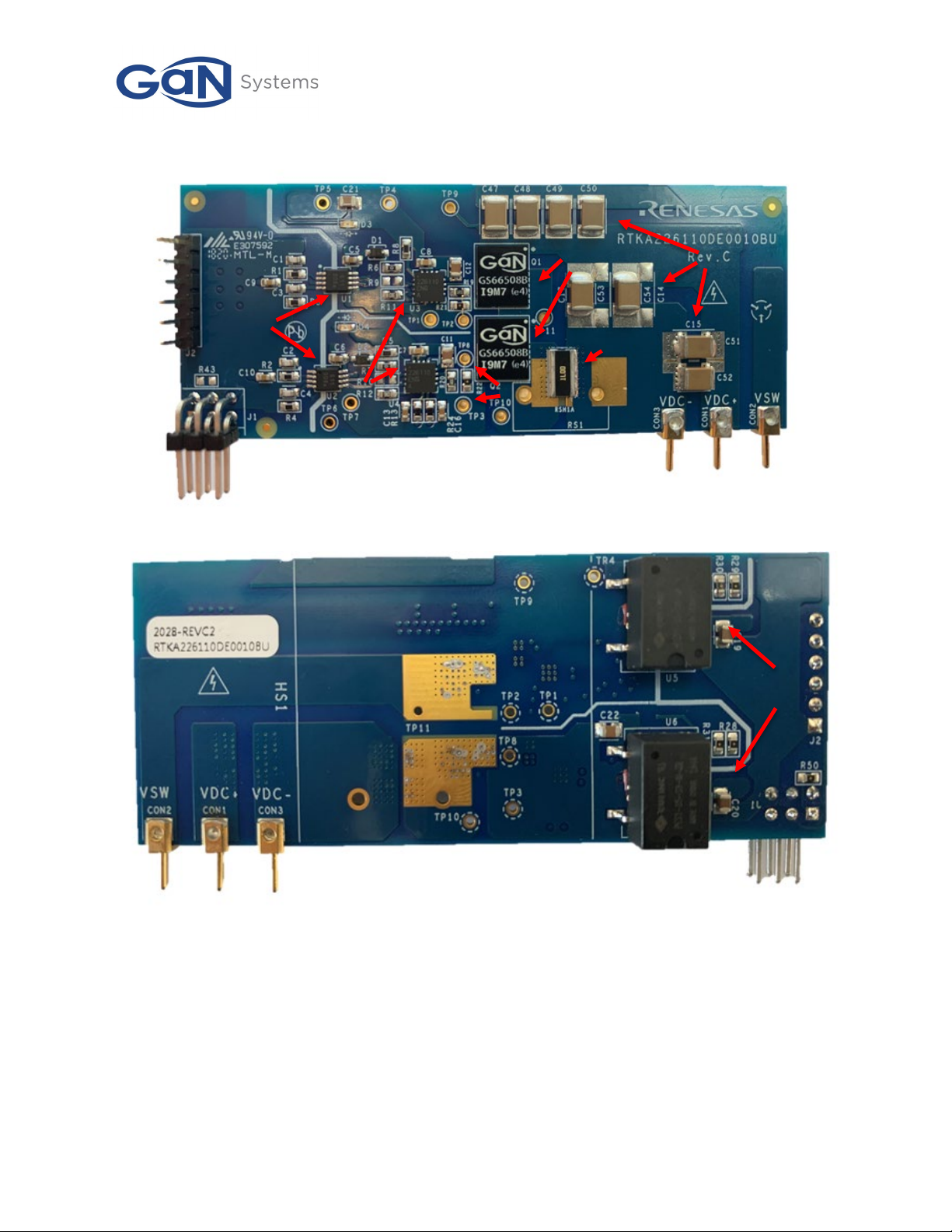
The GS-EVB-HB-66508B-RN is a RTK226110DE0010BU RAA226110
https://www.renesas.com/products/raa226110 gate drive demo board following GS665XXX-EVBDB
daughter board style. This evaluation kit consists of two GaN Systems 650V GaN Enhancement-mode
HEMTs (E-HEMTs) and all necessary circuits including half bridge gate drivers, isolated power supplies
and optional heatsink to form a functional half bridge power stage. It allows users to easily evaluate the
GaN E-HEMT performance in any half bridge-based topology, either with the universal mother board
(P/N: GS665MB-EVB) or users’ own system design. The GS-EVB-HB-66508B-RN demo board provides 0V
turn-off voltage solution. 0V turn-off solution is normally used in low power application. 0V turn-off
solution is easy to implement as there is no need a negative power supply rail. And the reverse
conduction voltage drop of GaN is lower. For E-mode GaN device the Vgs threshold voltage is low (typ:
1.7V). 0V turn-off has the risk of false turn-on when the GaN device is in off state. Also, the switching-off
loss will be higher than negative turn-off voltage. The 0V turn-off solution is normally used in the low
power applications.
Features:
•Serves as a reference design and evaluation tool as well as deployment-ready solution for easy in-
system evaluation.
•Vertical mount style with height of 35mm, which fits in majority of 1U design and allows
evaluation of GaN E-HEMT in traditional through-hole type power supply board.
•Current shunt position for switching characterization testing
•Universal form factor and footprint for all products
•0V turn off voltage
The daughter board and universal mother board ordering part numbers are below:
Table 1 Ordering part numbers
GS-EVB-HB-66508B-RN GS66508B GaN E-HEMT 650V/30A, 50mΩ With
RAA226110 gate driver, 0V turn off voltage
Universal 650V Mother Board
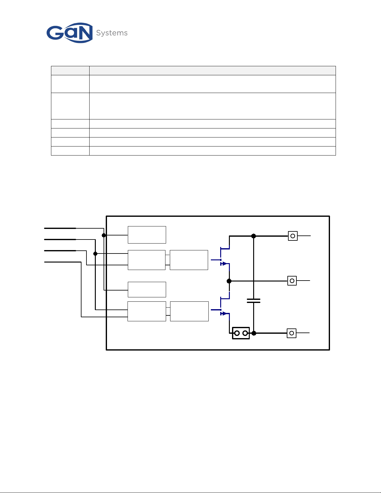
Control and Power I/Os:
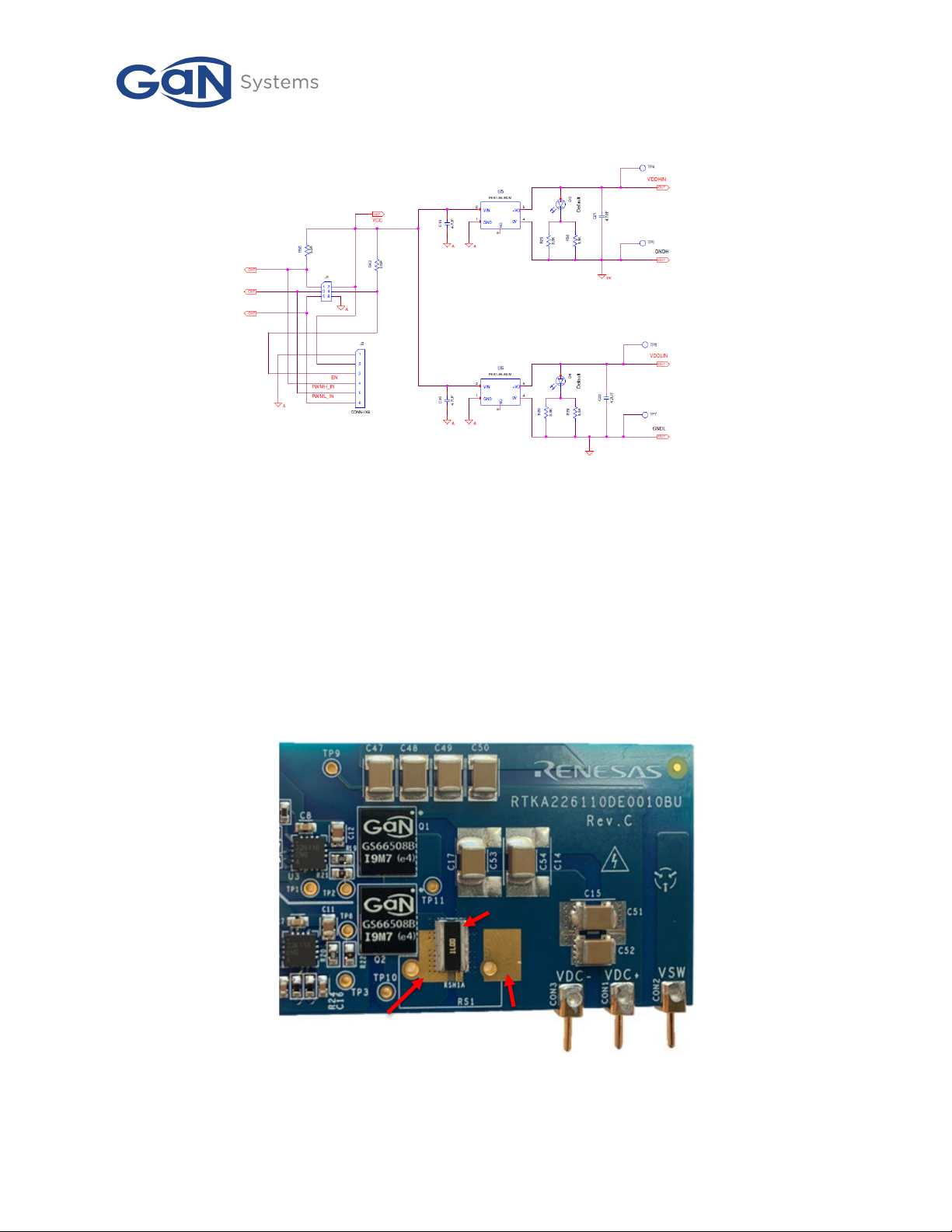
The daughter board GS-EVB-HB-66508B-RN circuit diagram is shown in Figure 1. The control logic
inputs on 2x3 pin header J1 are listed below: