Gan Systems GS-EVB-HB-0650603B-HD User manual

GS-EVB-HB-0650603B-HD
Half Bridge Bipolar Drive Switch Board
Technical Manual
_____________________________________________________________________________________________________________________
GS-EVB-HB-0650603B-HD TM Rev. 210712 © 2021 GaN Systems Inc www.gansystems.com 1
Please refer to the Evaluation Board/Kit Important Notice on page # 16
GS-EVB-HB-0650603B-HD
Half Bridge Bipolar Drive Switch Board
Technical Manual
Visit www.gansystems.com for the latest version of this technical manual.

GS-EVB-HB-0650603B-HD
Half Bridge Bipolar Drive Switch Board
Technical Manual
_____________________________________________________________________________________________________________________
GS-EVB-HB-0650603B-HD TM Rev. 210712 © 2021 GaN Systems Inc www.gansystems.com 2
Please refer to the Evaluation Board/Kit Important Notice on page # 16
DANGER
DO NOT TOUCH THE BOARD WHEN IT IS ENERGIZED AND ALLOW ALL
COMPONENTS TO DISCHARGE COMPLETELY PRIOR HANDLING THE BOARD.
HIGH VOLTAGE CAN BE EXPOSED ON THE BOARD WHEN IT IS CONNECTED
TO POWER SOURCE. EVEN BRIEF CONTACT DURING OPERATION MAY
RESULT IN SEVERE INJURY OR DEATH.
Please sure that appropriate safety procedures are followed. This evaluation kit
is designed for engineering evaluation in a controlled lab environment and
should be handled by qualified personnel ONLY. Never leave the board
operating unattended.
WARNING
Some components can be hot during and after operation. There is NO built-in
electrical or thermal protection on this evaluation kit. The operating voltage,
current, and component temperature should be monitored closely during
operation to prevent device damage.
CAUTION
This product contains parts that are susceptible to damage by electrostatic
discharge (ESD). Always follow ESD prevention procedures when handling the
product.

GS-EVB-HB-0650603B-HD
Half Bridge Bipolar Drive Switch Board
Technical Manual
_____________________________________________________________________________________________________________________
GS-EVB-HB-0650603B-HD TM Rev. 210712 © 2021 GaN Systems Inc www.gansystems.com 3
Please refer to the Evaluation Board/Kit Important Notice on page # 16
Contents
1Overview..............................................................................................................................................................5
1.1 Introduction ...............................................................................................................................................5
1.2 Quick Start Guide......................................................................................................................................5
2Technical Description.........................................................................................................................................6
2.1 Gate Pull Up and Pull Down Resistors ..................................................................................................6
2.2 Enable and Start Sequence .......................................................................................................................6
2.3 Measurement Points .................................................................................................................................7
2.4 Bipolar Gate Drive.....................................................................................................................................7
2.5 Propagation Delay.....................................................................................................................................8
3Test results ...........................................................................................................................................................9
3.1 Double pulse test.......................................................................................................................................9
3.2 Components Specification......................................................................................................................10
3.3 DPT Result 100V –15A...........................................................................................................................11
3.4 DPT Result 400V –62A...........................................................................................................................11
4Schematic ...........................................................................................................................................................12
5Layout.................................................................................................................................................................13
6Bill of Materials .................................................................................................................................................14
7Disclaimer ..........................................................................................................................................................15

GS-EVB-HB-0650603B-HD
Half Bridge Bipolar Drive Switch Board
Technical Manual
_____________________________________________________________________________________________________________________
GS-EVB-HB-0650603B-HD TM Rev. 210712 © 2021 GaN Systems Inc www.gansystems.com 4
Please refer to the Evaluation Board/Kit Important Notice on page # 16
List of Figures
Figure 1: GS-EVB-HB-0650603B-HD Quick Start ...................................................................................................5
Figure 2: HEY1011-L12C Wired-AND enable ........................................................................................................6
Figure 3: HEY1011-L12C Start up sequence............................................................................................................7
Figure 4: Measurements points.................................................................................................................................7
Figure 5: Bi-polar gate drive schematic ...................................................................................................................8
Figure 6: Typical Driver output at 100kHz .............................................................................................................9
Figure 7: Double Pulse Test.......................................................................................................................................9
Figure 8: Double Pulse Test Waveforms................................................................................................................10
Figure 9: DPT 100V –15A........................................................................................................................................11
Figure 10: DPT 400V –62A......................................................................................................................................11
Figure 11: GS-EVB-HB-0650603B-HD Schematic .................................................................................................12
Figure 12: GS-EVB-HB-0650603B-HD Silkscreen and component placement..................................................13
Figure 13: GS-EVB-HB-0650603B-HD Top Side Copper (L) and Layer 2 Copper (R) .....................................13
Figure 14: GS-EVB-HB-0650603B-HD Layer 3 Copper(L) and Bottom Side Copper (R) ................................13
List of Tables
Table 1: Bill of materials..........................................................................................................................................14

GS-EVB-HB-0650603B-HD
Half Bridge Bipolar Drive Switch Board
Technical Manual
_____________________________________________________________________________________________________________________
GS-EVB-HB-0650603B-HD TM Rev. 210712 © 2021 GaN Systems Inc www.gansystems.com 5
Please refer to the Evaluation Board/Kit Important Notice on page # 16
1Overview
1.1 Introduction
The Integrated Circuits Half Bridge Driver-Switch GS-EVB-HB-0650603B-HD is a demonstration board
containing two HEY1011-L12C GaN FET drivers and two 650V, 60A GaN FETs configured in a half bridge
configuration.
The datasheet for the HEY1011-L12C in this board can be found here.
The GS-EVB-HB-0650603B-HD can be used to perform double pulse tests, or to interface the half bridge to
an existing LC power section, both as shown below.
The isolated HEY1011-L12C driver does not require secondary side power or bootstrap components. Gate
drive power is supplied to secondary side from the primary side supply voltage VDRV. The amplitude of
the gate drive can be varied by varying VDRV between 7 V and 15 V.
1.2 Quick Start Guide
Figure 1: GS-EVB-HB-0650603B-HD Quick Start
1. Apply VDRV = 12V
2. Link pins EN_PU and EN (if not using external Enable control)
3. Apply input gate signals, with adequate dead time, to the IN_L and IN_H inputs.
4. Convenient test points a located on the test board as shown above. A suitable differential
oscilloscope should be used to monitor the high side gate signal from VGH to VSW.
VDRV
IN_H
IN_L
LINK
VBUS
LOUT
COUT
Optional external
decoupling

GS-EVB-HB-0650603B-HD
Half Bridge Bipolar Drive Switch Board
Technical Manual
_____________________________________________________________________________________________________________________
GS-EVB-HB-0650603B-HD TM Rev. 210712 © 2021 GaN Systems Inc www.gansystems.com 6
Please refer to the Evaluation Board/Kit Important Notice on page # 16
2Technical Description
2.1 Gate Pull Up and Pull Down Resistors
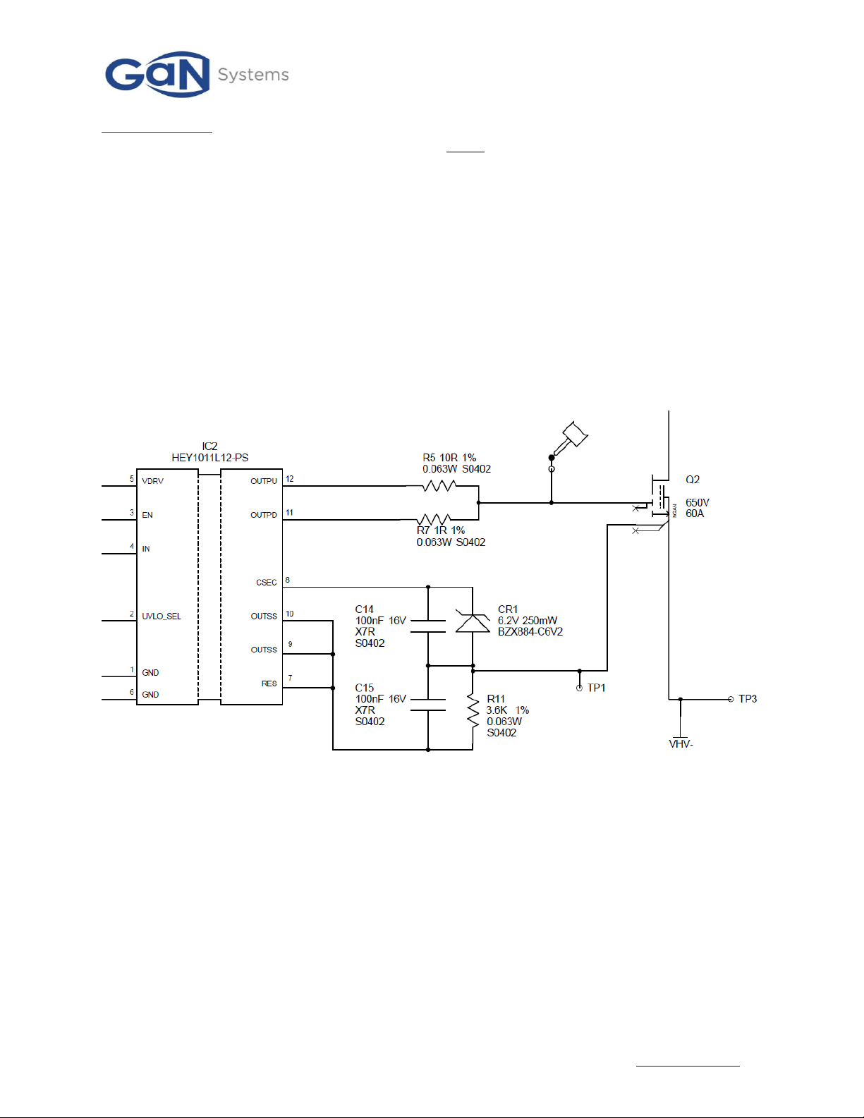
The HEY1011-L12C gate driver has independent output pins for the gate pull up and gate pull down
allowing control of the turn-on and turn-off rise and fall times.
The default values for these resistors are:
•OUTPU: R1 and R5 = 10 Ohms
•OUTPD: R3 and R7 = 1 Ohm
These values can be modified to suit your own application.
2.2 Enable and Start Sequence
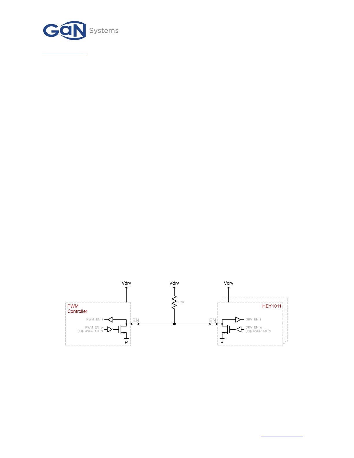
The HEY1011-L12C has an open drain enable pin (EN) to facilitate a system level wired-AND start up.
When the enable pin is externally pulled low this forces the driver into a low power mode. The driver
output is pulled low in this mode. In the event of an internal fault condition, such as UVLO, this pin is
actively pulled low internally by the driver. During normal operation, the pin is released by the driver, and
must be pulled high with an external pull-high resistor. This functionality can be used by the PWM
controller as an indication that it can start sending IN pulses to the driver. It is typically wired AND with
the controller enable pin as shown in Figure 2 below.
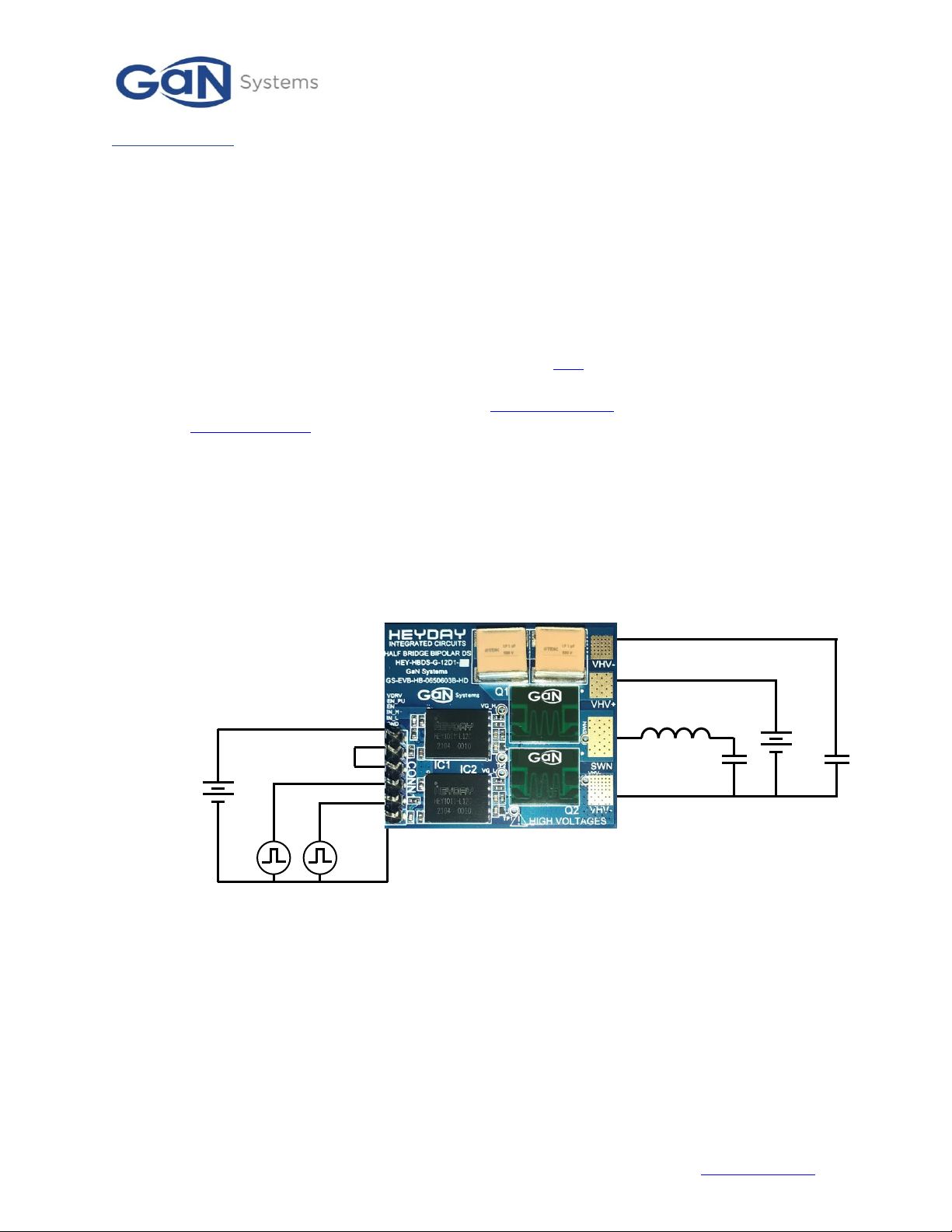
The GS-EVB-HB-0650603B-HD evaluation board provides direct access to the EN pin on connector
CONN1. Internally the board contains a 100k pull up resistor connected from VDRV to the EN_PU pin on
connector CONN1 –see schematic in Figure 11. If external control of the enable function is not required,
pins EN and EN_PU must be linked together on CONN1 to make use of the internal 100k pull up resistor
to enable the driver. If the EN pin is left floating, the drivers will not respond to INL or INH input signals.
Figure 2: HEY1011-L12C Wired-AND enable
The start up sequence of the HEY1011-L12C is shown in Figure 3 below. Time TSTART is defined as the time
after which VDRV reaches the UVLO rising level to the HEY1011-L12C releasing the EN internal pull down.
IMPORTANT the IN signal must not be applied before the EN pin has been released.

GS-EVB-HB-0650603B-HD
Half Bridge Bipolar Drive Switch Board
Technical Manual
_____________________________________________________________________________________________________________________
GS-EVB-HB-0650603B-HD TM Rev. 210712 © 2021 GaN Systems Inc www.gansystems.com 7
Please refer to the Evaluation Board/Kit Important Notice on page # 16
Figure 3: HEY1011-L12C Start up sequence.
2.3 Measurement Points
The GS-EVB-HB-0650603B-HD EVB contains convenient test points for monitoring the high and low side
gate drives as well as the switch node as shown in Figure 4 below.
When measuring VGS_H use a differential probe with suitable ratings for the applied bus voltage. The GS-
EVB-HB-0650603B-HD EVB uses a bipolar gate drive arrangement as shown in Figure 5 below. When
measuring VGS, both gate drives are measured relative to the source of their associated GaN FET. Therefore,
the off-state voltage will be negative.
It is important to use a low inductance scope probe ground lead as shown to avoid pickup of spurious
switching noise.
2.4 Bipolar Gate Drive
Due to the high rate of change of voltages and currents in power switching circuits, unwanted inductor
currents and capacitor voltage drops can be created.
One such example is the false turn on of a FET due to a dv/dt event. In a half bridge circuit, after the low
side FET has been turned off and a suitable dead-time elapsed, the high side FET is turned on. This
produces a rapidly changing switch node voltage at the drain of the low side FET. This voltage will
produce a capacitor current:
VGS_H
VGS_L
SWN
Low inductance
scope measurement
Figure 4: Measurements points

GS-EVB-HB-0650603B-HD
Half Bridge Bipolar Drive Switch Board
Technical Manual
_____________________________________________________________________________________________________________________
GS-EVB-HB-0650603B-HD TM Rev. 210712 © 2021 GaN Systems Inc www.gansystems.com 8
Please refer to the Evaluation Board/Kit Important Notice on page # 16
flowing in the gate-drain capacitance, CGD, and driver output. It will cause the voltage on the gate of the
low side FET to rise. If this voltage spike peaks beyond the threshold voltage VTH, the FET will conduct.
Considering that the high side FET is also conducting, this can result in a potentially destructive shoot-
through event.
The GS-EVB-HB-0650603B-HD EVB uses a bipolar gate drive arrangement which is useful to mitigate
against the effects of gate-drain capacitor currents. The secondary supply voltage VSEC is a function of the
primary supply voltage VDRV. The zener diode, CR1, will regulate the positive turn on voltage of the GaN
FET. During the turn-off of period, the gate voltage will be negative with a value of:
VGS_OFF = VSEC –VZENER. VSEC is typically 9 V.
This negative VGS_OFF voltage allows more margin before the threshold voltage can be reached.
Figure 5: Bi-polar gate drive schematic
2.5 Propagation Delay
•VDRV = 12V
•Input = 100kHz
•RPU = 10R, RPD = 1R
•Power train un-loaded. That is, VHV+ = 0V.

GS-EVB-HB-0650603B-HD
Half Bridge Bipolar Drive Switch Board
Technical Manual
_____________________________________________________________________________________________________________________
GS-EVB-HB-0650603B-HD TM Rev. 210712 © 2021 GaN Systems Inc www.gansystems.com 9
Please refer to the Evaluation Board/Kit Important Notice on page # 16
CH2: Low side driver input
CH1: Low side driver (IC2) output wrt VHV-
CH2: Low side driver input
CH1: Low side driver (IC2) output wrt VHV-
CH2: Low side driver input
CH1: Low side driver (IC2) output wrt VHV-
Low side driver output
Typical Turn-on Propagation Delay
Typical Turn-off Propagation Delay
Figure 6: Typical Driver output at 100kHz
3Test results
3.1 Double pulse test
The double pulse test is used to evaluate the switching characteristics of a power switch under hard
switching but in a safe manner.
For a low side switch the setup is as shown below:
Figure 7: Double Pulse Test
The low side switch is driven with two pulses as shown below. The high side switch can be held off or
driven with the inverse of the low side gate switch (with adequate dead time).

GS-EVB-HB-0650603B-HD
Half Bridge Bipolar Drive Switch Board
Technical Manual
_____________________________________________________________________________________________________________________
GS-EVB-HB-0650603B-HD TM Rev. 210712 © 2021 GaN Systems Inc www.gansystems.com 10
Please refer to the Evaluation Board/Kit Important Notice on page # 16
Figure 8: Double Pulse Test Waveforms
An inductor is placed in parallel with the high side switch. The goal of this inductor is to establish the test
level current in the low side switch at the end of the first on pulse (1). The magnitude of the test level
current at the end of period 1 is given by:
During period 2, the inductor current will naturally decay. The duration of period 2 should not be too long
that inductor current deviates significantly from the desired test level.
During period 3, the inductor current will again rise. Period 3 should not be so long that the inductor
current rises to an excessive level.
The falling edge of pulse 1 is used to examine the hard turn off characteristics of the switch. The rising
edge of pulse 3 is used to examine the hard turn on characteristics of the switch. By only applying these
two pulses, the switches are only on for a very short time and should not overheat.
3.2 Components Specification
COMPONENTS
Drivers:
Heyday HEY1011-L12C
Inductor:
49uH 360mΩAir Core
RPU:
10
RPD:
1
VDS
IL
VGS_L
123
Test level
current
Hard switching edges
IDS

GS-EVB-HB-0650603B-HD
Half Bridge Bipolar Drive Switch Board
Technical Manual
_____________________________________________________________________________________________________________________
GS-EVB-HB-0650603B-HD TM Rev. 210712 © 2021 GaN Systems Inc www.gansystems.com 11
Please refer to the Evaluation Board/Kit Important Notice on page # 16
3.3 DPT Result 100V –15A
CH1 (Red): Low side output wrt VHV-
CH2 (Grn): Switch Node (500MHz Probe)
CH4 (Blu): Inductor Current (1A/V)
CH1 (Red): Low side output wrt VHV-
CH2 (Grn): Switch Node (500MHz Probe)
CH4 (Blu): Inductor Current (1A/V)
CH1 (Red): Low side output wrt VHV-
CH2 (Grn): Switch Node (500MHz Probe)
CH4 (Blu): Inductor Current (1A/V)
DPT Overview
DPT Hard switching turn off
DPT Hard switching turn on
Time base (12.5ns/div)
Figure 9: DPT 100V –15A
3.4 DPT Result 400V –62A
CH1 (Red): Low side output wrt VHV-
CH2 (Grn): Switch Node (500MHz Probe)
CH4 (Blu): Inductor Current (1A/V)
CH1 (Red): Low side output wrt VHV-
CH2 (Grn): Switch Node (500MHz Probe)
CH4 (Blu): Inductor Current (1A/V)
CH1 (Red): Low side output wrt VHV-
CH2 (Grn): Switch Node (500MHz Probe)
CH4 (Blu): Inductor Current (1A/V)
DPT Overview
DPT Hard switching turn off
DPT Hard switching turn on
Time base (12.5ns/div)
Figure 10: DPT 400V –62A

GS-EVB-HB-0650603B-HD
Half Bridge Bipolar Drive Switch Board
Technical Manual
_____________________________________________________________________________________________________________________
GS-EVB-HB-0650603B-HD TM Rev. 210712 © 2021 GaN Systems Inc www.gansystems.com 12
Please refer to the Evaluation Board/Kit Important Notice on page # 16
4Schematic
Figure 11: GS-EVB-HB-0650603B-HD Schematic

GS-EVB-HB-0650603B-HD
Half Bridge Bipolar Drive Switch Board
Technical Manual
_____________________________________________________________________________________________________________________
GS-EVB-HB-0650603B-HD TM Rev. 210712 © 2021 GaN Systems Inc www.gansystems.com 13
Please refer to the Evaluation Board/Kit Important Notice on page # 16
5Layout
Figure 12: GS-EVB-HB-0650603B-HD Silkscreen and component placement
Figure 13: GS-EVB-HB-0650603B-HD Top Side Copper (L) and Layer 2 Copper (R)
Figure 14: GS-EVB-HB-0650603B-HD Layer 3 Copper(L) and Bottom Side Copper (R)

GS-EVB-HB-0650603B-HD
Half Bridge Bipolar Drive Switch Board
Technical Manual
_____________________________________________________________________________________________________________________
GS-EVB-HB-0650603B-HD TM Rev. 210712 © 2021 GaN Systems Inc www.gansystems.com 14
Please refer to the Evaluation Board/Kit Important Notice on page # 16
6Bill of Materials
Table 1: Bill of materials
Item
Ref Name
Description
Value
Qty
Manufacturer
Manufacturer PN
1
C1, C2
CAP CERALINK, 1uF,500V
PLZT
1uF
2
TDK
B58031U5105M062
2
C14,C15,C16,C17
CAP, CER,100nF,16V,X7R, S0402
100nF
4
KEMET
C0402C104K4RALTU
3
C3,C4
CAP, CER, 75pF,50V,NP0, S0402
75pF
2
KEMET
C0402C750J5GACTU
4
C6,C13
CAP, CER,1uF,25V,X5R, S0402
1uF
2
MURATA
GRM155R61E105KA12
D
3
CONN1
HEADER, 6 WAY, 2.54mm
6WAY, 2P54
1
WURTH
61300611121
6
CR1,CR2
DIO ZEN, 6V2, 250mW, 2%,
SOD882
BZX884-C6V2
2
NEXPERIA
BZX884-B6V2,315
7
IC1,IC2
GaN FET Driver
HEY1011-L12C
2
HEYDAY IC
HEY1011-L12C
8
Q1,Q2
NGAN 650V 60A
NGAN 650V 60A
2
GAN SYSTEMS
NGAN 650V 60A
9
R1,R5
RES, SMD, 10R, 0.063W, 1%,
S0402
10R
2
VISHAY
CRCW040210R0FKED
10
R11,R13
RES, SMD, 3K6, 0.063W, 1%,
S0402
3.6K
2
PANASONIC
ERJ2RKF3601X
11
R2
RES, SMD, 100K, 0.063W, 1%,
S0402
100K
1
PANASONIC
ERJ2GEJ104X
12
R3,R7
RES, SMD, 1R0, 0.063W, 1%,
S0402
1R
2
VISHAY
CRCW04021R00FKED
13
R4,R8
RES, SMD, 0R0, 0.063W, 1%,
S0402
0R
2
VISHAY
RCG04020000Z0ED
14
R6,R9
RES, SMD, 49R9, 0.063W, 1%,
S0402
49R9
2
VISHAY
CRCW040249R9FKED

GS-EVB-HB-0650603B-HD
Half Bridge Bipolar Drive Switch Board
Technical Manual
_____________________________________________________________________________________________________________________
GS-EVB-HB-0650603B-HD TM Rev. 210712 © 2021 GaN Systems Inc www.gansystems.com 15
Please refer to the Evaluation Board/Kit Important Notice on page # 16
7Disclaimer
Heyday Integrated Circuits (“Heyday”) provides all data in any resource and in any format such as, but
not limited to datasheets, reference designs, application notes, web tools and safety information “as is” and
with all faults, and disclaims any type of warranties, fitness for a particular purpose or non-infringement
of 3rd party intellectual property rights. Any examples described herein are for illustrative purposes only
and are intended to provide customers with the latest, accurate, and in-depth documentation regarding
Heyday products and their potential applications. These resources are subject to change without notice.
Heyday allows you to use these resources only for development of an application that uses the Heyday
product(s) described in the resource. Other reproduction and display of these resources are prohibited.
Heyday shall have no liability for the consequences of use of the information supplied herein.

GS-EVB-HB-0650603B-HD
Half Bridge Bipolar Drive Switch Board
Technical Manual
_____________________________________________________________________________________________________________________
GS-EVB-HB-0650603B-HD TM Rev. 210712 © 2021 GaN Systems Inc www.gansystems.com 16
Please refer to the Evaluation Board/Kit Important Notice on page # 16
Evaluation Board/kit Important Notice
GaN Systems Inc. (GaN Systems) provides the enclosed product(s) under the following AS IS conditions:
This evaluation board/kit being sold or provided by GaN Systems is intended for use for ENGINEERING
DEVELOPMENT, DEMONSTRATION, and OR EVALUATION PURPOSES ONLY and is not considered by GaN
Systems to be a finished end-product fit for general consumer use. As such, the goods being sold or provided are
not intended to be complete in terms of required design-, marketing-, and/or manufacturing-related protective
considerations, including but not limited to product safety and environmental measures typically found in end
products that incorporate such semiconductor components or circuit boards. This evaluation board/kit does not fall
within the scope of the European Union directives regarding electromagnetic compatibility, restricted substances
(RoHS), recycling (WEEE), FCC, CE or UL, and therefore may not meet the technical requirements of these directives,
or other related regulations.
If this evaluation board/kit does not meet the specifications indicated in the Technical Manual, the board/kit may be
returned within 30 days from the date of delivery for a full refund. THE FOREGOING WARRANTY IS THE
EXCLUSIVE WARRANTY MADE BY THE SELLER TO BUYER AND IS IN LIEU OF ALL OTHER WARRANTIES,
EXPRESSED, IMPLIED, OR STATUTORY, INCLUDING ANY WARRANTY OF MERCHANTABILITY OR FITNESS
FOR ANY PARTICULAR PURPOSE. EXCEPT TO THE EXTENT OF THIS INDEMNITY, NEITHER PARTY SHALL
BE LIABLE TO THE OTHER FOR ANY INDIRECT, SPECIAL, INCIDENTAL, OR CONSEQUENTIAL DAMAGES.
The user assumes all responsibility and liability for proper and safe handling of the goods. Further, the user
indemnifies GaN Systems from all claims arising from the handling or use of the goods. Due to the open construction
of the product, it is the user’s responsibility to take any and all appropriate precautions with regard to electrostatic
discharge.
No License is granted under any patent right or other intellectual property right of GaN Systems whatsoever. GaN
Systems assumes no liability for applications assistance, customer product design, software performance, or
infringement of patents or any other intellectual property rights of any kind.
GaN Systems currently services a variety of customers for products around the world, and therefore this transaction
is not exclusive.
Please read the Technical Manual and, specifically, the Warnings and Restrictions notice in the Technical Manual
prior to handling the product. Persons handling the product(s) must have electronics training and observe good
engineering practice standards.
This notice contains important safety information about temperatures and voltages. For further safety concerns,
please contact a GaN Systems’ application engineer.

GS-EVB-HB-0650603B-HD
Half Bridge Bipolar Drive Switch Board
Technical Manual
_____________________________________________________________________________________________________________________
GS-EVB-HB-0650603B-HD TM Rev. 210712 © 2021 GaN Systems Inc www.gansystems.com 17
Please refer to the Evaluation Board/Kit Important Notice on page # 16
In Canada:
GaN Systems Inc.
1145 Innovation Drive Suite 101
Ottawa, Ontario, Canada K2K 3G8
T +1 613-686-1996
In Europe:
GaN Systems Ltd., German Branch
Terminalstrasse Mitte 18,
85356 München, Germany
T +49 (0) 8165 9822 7260
In the United States:
GaN Systems Corp. 2723 South State Street,
Suite 150, Ann Arbor, MI. USA 48104 T +1
248-609-7643
www.gansystems.com
Important Notice –Unless expressly approved in writing by an authorized representative of GaN Systems, GaN Systems components are not designed, authorized
or warranted for use in lifesaving, life sustaining, military, aircraft, or space applications, nor in products or systems where failure or malfunction may result in
personal injury, death, or property or environmental damage. The information given in this document shall not in any event be regarded as a guarantee of
performance. GaN Systems hereby disclaims any or all warranties and liabilities of any kind, including but not limited to warranties of non-infringement of
intellectual property rights. All other brand and product names are trademarks or registered trademarks of their respective owners. Information provided herein
is intended as a guide only and is subject to change without notice. The information contained herein or any use of such information does not grant, explicitly, or
implicitly, to any party any patent rights, licenses, or any other intellectual property rights. General Sales and Terms Conditions apply.
© 2009-2019 GaN Systems Inc. All rights reserved.

Table of contents