Gecko CLK036 Supplement

GEKCO Inc.
1565 SW Cypress Ln
McMinnville, OR 97128
(503) 472-4770 P/N 595-324 REV 1.0
Copyright 2018
GEKCO Inc.
All Rights Reserved
Printed in the United States of America
c
GEKCO
DIGITAL CLOCK
MODEL CLK036
ASSEMBLY & OPERATION MANUAL

This page is intentionally left blank

GEKCO DIGITAL CLOCK P/N CLK036 ASSEMBLY & OPERATION MANUAL
GEKCO INC. Rev 1.0 1
TABLE OF CONTENTS
1. INTRODUCTION................................................................................................................................................ 3
2. OPERATIONAL SUMMARY.......................................................................................................................... 3
3. PARTS AND UNPACKING.............................................................................................................................. 4
3.1. TOP LEVELPARTS LIST ...................................................................................................................................... 4
3.2. DISPLAY BOARD PARTS LIST.............................................................................................................................. 5
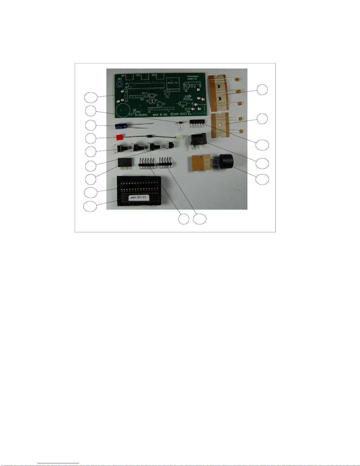
3.3. MAIN BOARD PARTS LIST................................................................................................................................... 5
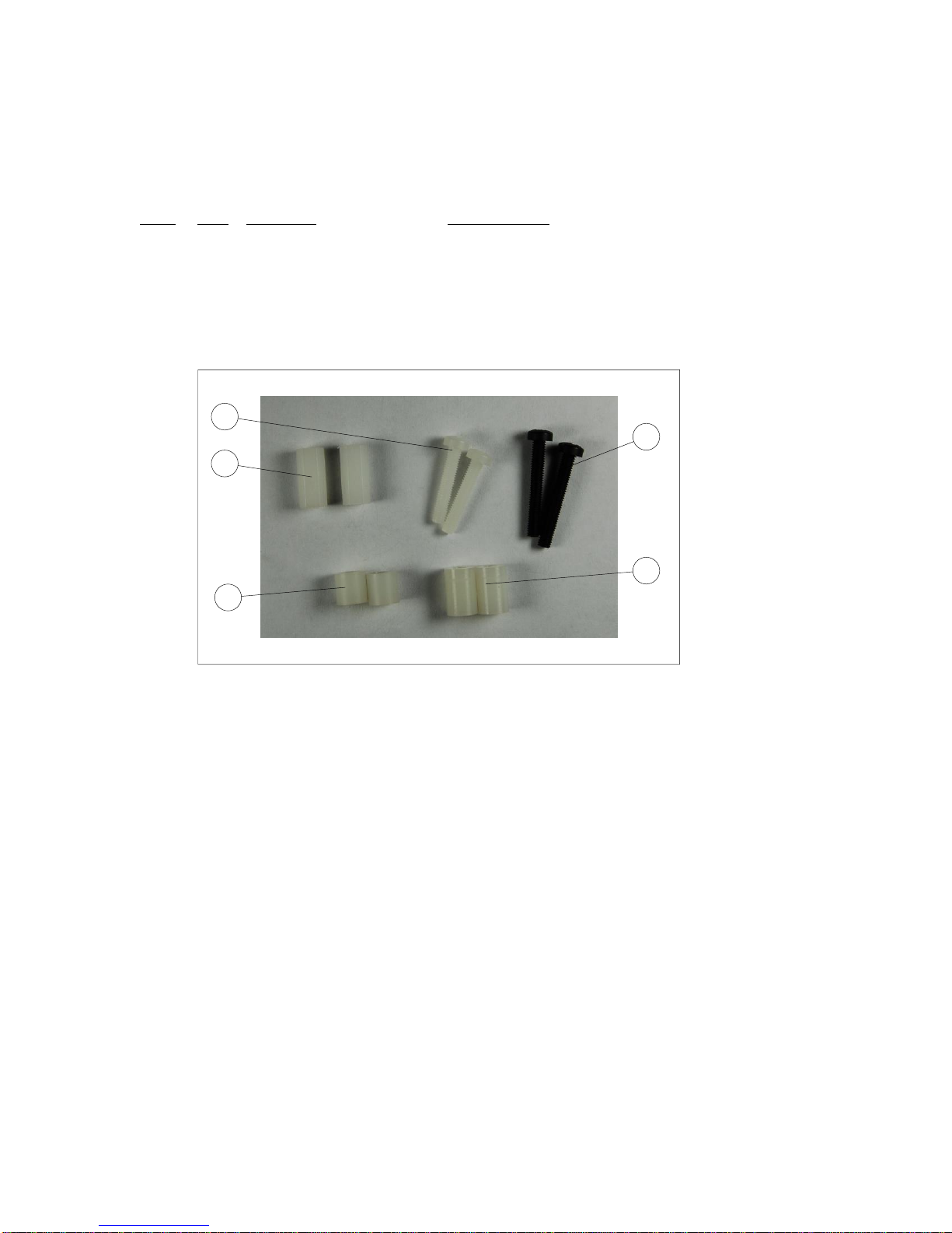
3.4. FINALASSEMBLY HARDWARE PARTS LIST....................................................................................................... 7
3.5. ENCLOSURE PARTS LIST..................................................................................................................................... 8
4. ASSEMBLY NOTES........................................................................................................................................... 9
4.1. TOOLS............................................................................................................................................................... 9
4.2. ASSEMBLY ...................................................................................................................................................... 9
4.3. SOLDERING..................................................................................................................................................... 9
5. STEP-BY-STEP ASSEMBLY .........................................................................................................................10
5.1. MAIN CIRCUITBOARD...................................................................................................................................... 10
6. INITIAL TESTS.................................................................................................................................................12
7. FINAL TESTS....................................................................................................................................................13
8. IN CASE OF DIFFICULTY ............................................................................................................................13
9. FINAL PCA ASSEMBLY................................................................................................................................13
10. FINAL ASSEMBLY......................................................................................................................................13
11. THEORY OF OPERATION.......................................................................................................................16
11.1. BLOCKDIAGRAM.............................................................................................................................................. 16
11.1. MAIN BOARD CIRCUIT DESCRIPTION............................................................................................................... 16
11.2. DISPLAY BOARD CIRCUITDESCRIPTION..........................................................................................................17
12. FIRMWARE ..................................................................................................................................................18
12.1. FLOWCHART ....................................................................................................................................................18
12.2. FIRMWARE DESIGN DESCRIPTION....................................................................................................................19
13. PCA PICTORIAL DIAGRAMS.................................................................................................................19
13.1. MAIN BOARD....................................................................................................................................................19
13.2. DISPLAY BOARD ...............................................................................................................................................20
14. SCHEMATIC MAIN BOARD....................................................................................................................22
15. SCHEMATIC DISPLAY BOARD............................................................................................................. 23
16. DOCUMENT REVISION HISTORY........................................................................................................ 24

GEKCO DIGITAL CLOCK P/N CLK036 ASSEMBLY & OPERATION MANUAL
2 REV 1.0 GEKCO INC.
LIST OF FIGURES
FIGURE 1:MAIN BOARD COMPLETED ASSEMBLY...............................................................................................10
FIGURE 2MAIN BOARD TOP VIEW1.................................................................................................................... 10
FIGURE 3:MAIN BOARD TOP VIEW2...................................................................................................................10
FIGURE 4:MAIN BOARD TOP VIEW3...................................................................................................................10
FIGURE 5:MAIN BOARD TOP VIEW4...................................................................................................................11
FIGURE 6:MAIN BOARD WITH STANDOFFS...........................................................................................................11
FIGURE 7:MAIN AND DISPLAY BOARD INTERFACE CONNECTOR MOUNTING.....................................................12
FIGURE 8RTCMODULE ASSEMBLY.................................................................................................................... 13
FIGURE 9ENCLOSURE BACK ................................................................................................................................14
FIGURE 10ENCLOSURE BACK WITH TOP .............................................................................................................14
FIGURE 11DISPLAY BOARD TOP SIDE .................................................................................................................20
FIGURE 12DISPLAY BOARD BOTTOM SIDE..........................................................................................................21

CLK036
GEKCO INC. Rev 1.0 3
1. Introduction
The Digital Clock Model CLK056 was designed to fill the need for an accurate digital clock with the
capabilities of two time zone displays in a compact format.
This clock has 6 digits for hours, minutes and seconds and the hours displaycan alternate between
two time zones, i.e. Coordinated Universal Time (UTC) and local time.
The CLK056 is offered in kit form or fullyassembled and tested. The kit is veryeasy to assemble with
no surface mount parts.
This step bystep manualwill guide you through the process to complete the assembly and testing of
the model CLK056 Digital Clock. The manual was designed so a totalbeginner in electronics can be
successful but the more experienced builder can skip any unnecessaryinformation. Also this design is
fullyopen source for both the hardware and firmware. There are full schematics and pictorial diagrams
of the hardware, also there are links and flowcharts of the firmware microcontroller code.
2. Operational Summary
The Model CLK036 has 8 digits of seven segment displays to displaytime zone one HOURS (UTC),
time zone 2 HOURS (local), MINUTES and SECONDS.
The eight digit displayprovides two time zones Hours, Hours, Minutes and Seconds
The displayLEDs are high contrast red, 0.36 inch character height
Adjustable displaybrightness
Local hours can be set for 12 or 24 hour mode
Veryaccurate Real Time Clock (RTC) with batterybackup
Powered by a U.L. listed 5 VDC walladapter
Size: 4.16 x 2.35 x 1.46 inches (Width x Heightx Depth)
Weight: 0.30 pounds

GEKCO DIGITAL CLOCK P/N CLK036 ASSEMBLY & OPERATION MANUAL
4 REV 1.0 GEKCO INC.
3. Parts and Unpacking
The kit is packaged in the order that the assemblyis recommended. Each assembly block has it’s
associated parts bag. Onlyopen a parts bag when called for during assemblyto avoid misplacing parts.
3.1. Top Level Parts List
Remove the parts from the main bag and separate each individual parts bags.
ITEM
QTY
PART NO.
DESCRIPTION
1
1
DBR836-KIT
Clock Display Board PCA parts kit
2
1
CLK036M-KIT
Clock Main Board PCA parts kit
3
1
2217625
Real Time Clock (RTC) Module DS3231
4
1
CLK036HDW-KIT
Final Assembly Hardware
5
1
CLK036ENC-KIT
Enclosure Acrylic 6 Piece
6
1
54-660
AC to DC Power SupplyWall Adapter Single
Output 5 Volt 1 Amp 5 Watt 2.1mm Conn

DIGITAL CLOCK MODEL CLK036
GEKCO INC. Rev 1.0 5
3.2. Display Board Parts List
Clock 036 Display Board PCA parts kit, DBR836-KIT
ITEM
QTY
PART NO.
DESCRIPTION
1
1
DBR836-PCA
LED DisplayModule Assembly7-Segment 8 Digit
0.36”
2
1
131-1X05
Connector Header Male 1 row of 5 pins
3
2
255-25511
Hardware Standoff Nylon M3 x 12 mm
4
4
255-29341
Hardware ScrewNylon M3 x 0.50 mm Thread,
6mm White
1
2
3 4
3.3. Main Board Parts List
Clock 036 Main Board PCA parts kit, CLK036M-KIT
ITEM
QTY
REFDES
PART NO.
DESCRIPTION
VALUE
1
3
C4,C5,C6
20-104
Cap mono Cer 50v radial lead
0.1UF
2
2
C1,C2
21-220
Cap mono Cer COG radial
lead
22pF 100v
3
1
C3
26-102
Cap elect alum radial lead
10uF/16v
4
1
Y1
404-160
Crystal HC49
16.00 MHz
5
1
D1
55-62
Diode schottky rectifier
1N5817-T
6
3
SW1,SW2,S
W3
64-1839
Switch MomentarySPST
7
1
SW4
64-1827
Switch Momentary5mm H
8
1
J5
131-1X05S
Connector Header Female
1 row of 5 pins
9
1
J2
131-1X06RA
Connector Header Right Angle
Male 1 row of 6
pins
10
1
J3
131-1X05RA
Connector Header Right Angle
Male 1 row of 5
pins
11
1
J1
134-002
Connector Power 2.1mm PCB
Mount
12
1
RN1
95-103
Res network 6 sip
10K 5 Res SIP
Package
13
1
X1
434-311
Socket IC
Dip28-300
14
1
U1
444-361-01
IC Microcontroller
Programmed
Part CLK036
V1.01

GEKCO DIGITAL CLOCK P/N CLK036 ASSEMBLY & OPERATION MANUAL
6 REV 1.0 GEKCO INC.
15
1
LS1
220-1420
Audio Piezo Transducer 30V
16
1
81-180912C
Printed Circuit Board
Main Board
1
2
3
4
5
6
7
8
9 10
11
12
13
14
15
16

DIGITAL CLOCK MODEL CLK036
GEKCO INC. Rev 1.0 7
3.4. Final Assembly Hardware Parts List
Clock 036 Final Assembly Hardware parts kit, P/N CLK036HDW-KIT
ITEM
QTY
PART NO.
DESCRIPTION
1
2
255-25511
Hardware Standoff Nylon M3 x 12 mm
2
2
255-29346
Hardware ScrewNylon M3 x 0.50 mm Thread,
16mm White
3
2
255-29347
Hardware ScrewNylon M3 x 0.50 mm Thread,
20mm Black
4
2
255-876
Hardware Spacer Round 0.25" Hole Size #4
5
2
255-877
Hardware Spacer Round 0.375" Hole Size #4
1
2
4
5
3

GEKCO DIGITAL CLOCK P/N CLK036 ASSEMBLY & OPERATION MANUAL
8 REV 1.0 GEKCO INC.
3.5. Enclosure Parts List
Clock 036 Enclosure kit, P/N CLK036ENC-KIT
ITEM
QTY
PART NO.
DESCRIPTION
1
1
86-18111901
Front Panel Acrylic 3mm Transparent Red
2
1
86-18111902
Back Panel Acrylic 3mm Clear
3
1
86-18111903
Top Panel Acrylic 3mm Clear
4
1
86-18111904
Bottom Panel Acrylic 3mm Clear
5
1
86-18111905
Left Side Panel Acrylic 3mm Clear
6
1
86-18111906
Right Side Panel Acrylic 3mm Clear
1
5
6
2
3
4

DIGITAL CLOCK MODEL CLK036
GEKCO INC. Rev 1.0 9
4. Assembly Notes
4.1. TOOLS
You will need these tools to assemble your kit.
Diagonal Cutters
Needle Nose Pliers
Flat Head Screwdriver
Philips Screwdriver (for the enclosure
only)
Pencil Soldering Iron (22 to 25
WATTS)
4.2. ASSEMBLY
1. Follow the instructions carefully. Read the
entire step before you perform each
operation.
2. Refer to the Pictorial and Detail Illustrations
for help in performing the assembly steps.
The illustrations are arranged in the proper
sequence, as called for in the assembly
steps.
3. Pictorials show the overall operation for a
group of assembly steps: Details generally
illustrate a single step. When you are
directed to refer to a certain Pictorial “for
the following steps,” continue using that
Pictorial until you are referred to another
Pictorial for another group of steps.
4. Position all parts as shown in the Pictorials.
5. Solder instructions are generally given only
at the end of a series of similar steps. You
may solder more often if you desire.
6. Each circuit part in an electronic kit has its
own reference designator (R3, C8, etc.).
Use these designators when you want to
identify the same part in the various
sections of the manual.
7. SAFETY WARNING: Avoid eye injury
when you cut off excessive lead
lengths. Wear safety glasses or
goggles and hold the leads so they
cannot fly toward your eyes.
4.3. SOLDERING
Soldering is one of the most important
operations you will perform while assembling
your kit. A good solder connection will form an
electrical connection between two parts such
as a component lead and a circuit board foil. A
bad solder connection could prevent an
otherwise well-assembled kit from operating
properly.
It is easy to make a good solder connection if
you follow a fewsimple rules:
Use the right type of soldering iron. A 22 to 25-
watt pencil soldering iron with a 1/8” or 3/16”
chisel or pyramid tip works best.
Keep the soldering iron tip clean. Wipe it often
on a wet sponge or cloth: then apply solder to
the tip to give the entire tip a wet look. This
process is called tinning, and it will protect the
tip and enable you to make good connections.
When solder tends to “ball” or does not stick to
the tip, the tip needs to be cleaned and re-
tinned.
NOTE: What solder to use, leaded or lead
free? The printed circuit boards in this kit are
plated with lead free solder so if you choose to
use lead free solder the complete assemblywill
be RoHS compliant. Regarding kits though, it is
more difficult to solder with lead free material
due to the higher melting temperature, so we
recommend using a rosin core, radio-type
solder (60/40) or (63/37) tin-lead content for all
of the soldering in this kit. If you decide to use
leaded solder, be careful to wash your hands
after soldering and never eat, drink or smoke,
until you wash thoroughly and you are done
soldering. Contain all materials that touched
leaded solder in a special container dedicated
for that purpose. This waste can be disposed
of at electronic-recycling events or contact your
waste management company

GEKCO DIGITAL CLOCK P/N CLK036 ASSEMBLY & OPERATION MANUAL
10 REV 1.0 GEKCO INC.
5. Step-By-Step Assembly
5.1. Main Circuit Board
Figure 1: Main Board Completed Assembly
Figure 2 Main Board Top View 1
( ) C4: 0.1 uF (104) radial-lead ceramic
capacitor
( ) C5: 0.1 uF (104) radial-lead ceramic
capacitor
( ) C6: 0.1 uF (104) radial-lead ceramic
capacitor
Figure 3: Main Board Top View 2
( ) C1: 22 pF (22) radial-lead ceramic
capacitor
( ) C2: 22 pF (22) radial-lead ceramic
capacitor
In the next step be sure to observe the correct
polarity as noted before and lay the capacitor
down against the board.
C3 SIDE VIEW
( ) C3: 10 uF radial-lead electrolytic
aluminum capacitor
Figure 4: Main Board Top View 3
( ) Y1: Crystal HC49 16 MHz
For the next step, be careful to position the end
with the dot or line towards the “square pad”
and tapered outline on the circuit board. After
you solder the first pin make sure the pins are

DIGITAL CLOCK MODEL CLK036
GEKCO INC. Rev 1.0 11
fully seated in their holes, solder the rest of the
pins to the foil.
( ) RN1: 10 k103 resistor pack.
NOTE: When you install the diode, be sure to
orient the diode correctly. Always match the
band on the diode with the band mark on the
circuit board. The circuit will not work properly if
a diode is installed backwards.
( ) D1: 1N5817 schottky diode
When installing the IC socket next, be sure to
align the notch on the socket with the notch on
the PCB silkscreen.
( ) X1: 28 pin DIP socket
Figure 5: Main Board Top View 4
( ) SW1: momentaryright angle switch
( ) SW2: momentaryright angle switch
( ) SW3: momentaryright angle switch
( ) SW4: momentaryswitch
( ) J2: Connector Header Male 6 pin right
angle mount
( ) J3: Connector Header Male 5 pin right
angle mount
In the next step, solder one pin and re-align the
connector if necessary and then solder the rest
of the pins. The connector needs to be aligned
with the silkscreen outline.
( ) J1: Connector Power 2.1mm
( ) LS1: Audio Piezo Speaker
( ) Solder the leads to the foil and cut off
the excess lead lengths.
The next step is to install the mating
connectors between the display board (J1) and
the main board (J5).
Open the display board parts kit and get the
following parts:
Quantity2 of:
M3 x 12 mm nylon standoffs
Quantity4 of:
M3 x 6 mm nylon screws
The displayboard
The displayboard connector
J1: Connector header male 5 pin
The main board connector
J5: Connector Header Female 5 pin
Refer to figure 10 and 11 for the next steps
Mount two M3 x 12 mm nylon standoffs with
two M3 x 6 mm nylon screws on the main
board as shown.
(2) M3x12
mm nylon
standoff
Figure 6: Main board with standoffs
Insert the 5 pin female connector into the main
board at J5.
Identify the long pins on the display board 5 pin
male connector J1 and insert into or mate with
J5 the 5 pin female connector.
Place the display board onto the two M3 x 12
mm nylon standoffs, with the 5 pin male
connector J5 inserted into J1 on the display
board and insert two M3 x 6 mm nylon screws
as shown.

GEKCO DIGITAL CLOCK P/N CLK036 ASSEMBLY & OPERATION MANUAL
12 REV 1.0 GEKCO INC.
DISPLAY
BOARD
J1
MAIN
BOARD
J4
Figure 7: Main and Display board Interface connector
mounting
Solder the pins of the display board connector
J1 on the display board and then do the same
for theconnector pins on the main board J5.
J1 is not installed in this version of the kit.
This completes the assembly of the Main
board.
CIRCUIT BOARD CHECKOUT
Carefully inspect the circuit boards for the
following problems.
( ) Unsoldered connections
( ) Poor solder connections
( ) Solder bridges between foil patterns
( ) Protruding leads which could touch
together
Refer to the illustration where the parts were
installed as you make the following visual
checks.
( ) Diodes for the proper type and
positioning of the banded end
( ) Electrolytic capacitors for the correct
position of the positive ( ) or a negative ( )
marked ends
6. Initial Tests
Before installing the IC’s perform the following
tests.
Using a multi-meter to measure resistance
perform the following checks.
Main Board
( ) Verify that the resistance with the
positive lead on D1 cathode ( the component
end with the band) and negative lead on the
ground pad TP1, is greater than 2k ohms.
IC INSTALLATION.
NOTE: You will install the following IC’s on the
main circuit board.
CAUTION: Integrated circuits (IC’s) are
complex electrical devices that perform many
complicated operations in a circuit. These
devices can be damaged during installation.
Read all of the following information before you
install the IC’s.
Some of the IC’s you will install in the following
steps are MOS {metal oxide semiconductor)
devices. Be sure they do not get damaged by
static electricity. Once you remove the IC from
the foam pad, do not let go of it or lay it down
until it is in its socket. Install it as follows. Read
all of the following steps before you pick up an
IC.
1. Pick up the IC and touch the foam pad with
both hands.
2. Hold the foam pad with one hand and
remove the IC with the other hand.
3. Continue to hold the IC with the one hand
and straighten any bent pins with the other
hand.
4. The pins on the IC’s may be bent out at an
angle, and if this is the case, they will not
line up with the holes in the IC socket or
circuit board pads. Lay the IC down on its
side as and very carefully roll it toward the
pins to bend the lower pins into line. Then
turn the IC over and bend the pins on the
other side in the same manner. Do not try
to install and IC without first bending the
pins as described. To do so may damage
the IC pins or the socket, causing an
intermittent contact.
Install the IC on the display circuit board. Be
sure to line up the dimple with the circuit board
silkscreen

DIGITAL CLOCK MODEL CLK036
GEKCO INC. Rev 1.0 13
Install the IC on the main circuit board:
( ) U1: ATMEGA328P IC
This completes the assembly.
7. Final Tests
Using a multi-meter to measure resistance
perform the following checks.
( ) Verify that the resistance with the
positive lead on U5 pin 20 and negative lead on
pin 10, is greater than 2k ohms.
( ) Connect the plug in transformer T1 to
power connector PS1 and plug into a wall
outlet and verify that the voltage with the
positive lead on U5 pin 20 and negative lead on
pin 10, is 5V.
8. In Case Of Difficulty
The “Visual Checks” that are provided below
will help you locate any difficulties that might
occur during the assembly and testing of your
Digital Clock. Additional “ In Case of Difficulty”
information is also provided in your Operation
Manual.
In an extreme case where you are unable to
resolve a difficulty, refer to the “Customer
Service” information at the back of the Manual.
VISUAL CHECKS
1. The majority of kits that fail are due to poor
solder connections. Therefore, you can
eliminate many difficulties by carefully
inspecting each connection to make sure it
is soldered as described in the solder
instructions section. Reheat any doubtful
connections.
2. Check the circuit board to be sure there
are no solder bridges between adjacent
connections.
3. Check capacitor values carefully. Be sure
the proper value part is installed at each
capacitor location and that the negative
( ) mark or a positive ( ) mark is
oriented correctly.
4. Check each resistor value carefully.
5. Be sure the correct diode is installed at
each location, and that the banded end is
positioned correctly.
6. Check the orientation and the correct part
number of the Integrated Circuits. Use the
pictorial diagrams as a reference.
9. Final PCA Assembly
( ) Locate the RTC module and install on
the clock main board as shown.
Figure 8 RTC Module Assembly
10. Final Assembly
Skip these steps if the enclosure is not used.
( ) Unpack the 6 piece enclosure which
includes a transparent red front piece, and
clear back, top, bottom and side panels.
( ) Remove the paper backing on all the
enclosure pieces.

GEKCO DIGITAL CLOCK P/N CLK036 ASSEMBLY & OPERATION MANUAL
14 REV 1.0 GEKCO INC.
( ) Locate the clear back panel and insert
two white screws into their respective mounting
holes and add two ¼” spacers. Lay this
assembly down on the work space with the
screw threads facing up.
Figure 9 Enclosure Back
( ) Insert the top panel of the enclosure
onto the main board assembly. Make sure the
switches properly align with the top piece of the
enclosure.
Figure 10 Enclosure Back with Top
( ) Add the main board assembly with the
top panel on to the screws and spacers.
( ) Insert the two M3 x 12mm hex
standoffs and secure to the two rear screws.
( ) Mate the display board to the main
board and make sure the connector in mated
properly.
( ) Add the left panel.
( ) Add the right panel and make sure the
hole is aligned with the power connect J1.
( ) Add the bottom panel.

DIGITAL CLOCK MODEL CLK036
GEKCO INC. Rev 1.0 15
( ) Install two spacers over the mounting
holes
( ) Add the front panel and make sure all
pieces are aligned properly.
( ) Add two black screws and loosely
tighten to secure the enclosure.
Congratulations you have successfully
completed the assembly of the unit and now
you can enjoy using a clock that you have
assembled yourself.

GEKCO DIGITAL CLOCK P/N CLK036 ASSEMBLY & OPERATION MANUAL
16 REV 1.0 GEKCO INC.
11. Theory of Operation
11.1. Block Diagram
MICROCONTROLLER
8 8 8 8 8 8
REAL TIME
CLOCK
HOURS MINUTES SECONDS
UTC/LOCAL
BUZZER
DISPLAY
DRIVER
MENU
SET
+
DISPLAY BOARD
MAIN BOARD
The clock consists of two modules, the main board and the display board. The clock was designed this
way to allow the same main board to use different display boards which could varyin size.
If maybe helpful to review the block diagram and schematics while reading the circuit descriptions.
11.1. Main Board Circuit Description
The main circuit board has the microcontroller, real time clock (RTC), switch inputs and connectors for
the displayboard, programming interface and the input power.
The microcontroller U3 is the heart of the clock. This design uses the popular Atmel ATMEGA328P.
This is a verypowerful microcontroller with 32Kbytes of flash memory, and 2Kbytes of SRAM as well as
numerous other peripherals. See the ATMEGA328P data sheet for details.

DIGITAL CLOCK MODEL CLK036
GEKCO INC. Rev 1.0 17
The crystal Y1 provides the clock for the microcontroller and C1 and C2 are required pad capacitors for
the crystal to operate. The display board interface connectors are J4 and J5. J5 is the only one used in
the model CLK036. This connector provides the standard serial peripheral interface (SPI) interface to
the display board. The signal SS is asserted low when serial data is present on the MISO signal. The
MISO signal is the serial data stream from the microcontroller to the MAX7219 on the display board.
The signal SCK provides the clock timing for the interface. More details of the SPI interface can be
found on the web.
Connector J3 provides the interface to the real time clock (RTC) module. The clock time accuracy and
the time keeping function are provided by the RTC module, which has a Maxim DS3231 real time clock.
This device uses a 3 wire, I2C interface to communicate with the microcontroller.
Connector J2 is the programming interface connector. This allows the firmware to be modified and the
ability to reprogram the microcontroller. The CLK036 main board looks just like a Arduino Uno and can
use the popular Arduino IDE.
The path for the input power for the clock is provided by connector J1. The input voltage should be 5V
+/- 5%. Diode D1 is a schottky diode which provides protection of the internal circuits if the polarity of
the applied voltage is incorrect.
Resistor network RN1 provides the 10kohm pull up resistors for the switch inputs SW1 through SW4.
SW1, SW2 and SW3 provide the clock setup capabilities and SW4 allows the user to reset the device.
The piezo electric buzzer LS1 provides an audible alert for the alarm function.
11.2. Display Board Circuit Description
The display board used in the model CLK036 utilizes the MAX7219 as the display driver and controller.
This part provides a 4 wire interface to the main board to interface to the 8 digit display. The LED
displays are multiplexed by the logic in the MAX7219. The microcontroller on the main board only
needs to communicate with the display board when a change in the display is desired.

GEKCO DIGITAL CLOCK P/N CLK036 ASSEMBLY & OPERATION MANUAL
18 REV 1.0 GEKCO INC.
12. Firmware
12.1. Flow Chart
SET ALARM
DISPLAY TIME
TOGGLE ALARM
SET LOCAL
TIME 12/24
SET DISPLAY
BRIGHTNESS
SET TIME
TOGGLE ALARM
ON/OFF
SET 12 HR DISPLAY
SET 24 HR DISPLAY
MENU
SET
SET
PLUS
SELECT HOURS
SELECT MINUTES
SELECT SECONDS
SET LOOP
SET
SET
INCREMENT HOURS
INCREMENT MINUTES
INCREMENT SECONDS
MENU
MENU
MENU
MENU
SET
MENU
SET
MENU
PLUS
MENU
SET
MENU LOOP
SELECT HOURS
SELECT MINUTES
SET
PLUS
MENU
PLUS
ALARM LOOP
RETURN TO
FUNCTION LOOP
INCREMENT HOURS
INCREMENT MINUTES RETURN TO
FUNCTION LOOP
RETURN TO FUNCTION
LOOP
MENU
MENU
MENU SET
PLUS
PLUS
30 SECOND TIME OUT
ON ALL FUNCTIONS
SET UTC
HOURS INCREMENT HOURS
PLUS
MENU
MENU
SET UTC
ON/OFF
MENU
SET MENU
TOGGLE UTC
ON/OFF
TIME IS FROZEN UNTIL
MENU IS PRESSED TO EXIT
TIME SET FUNCTION
+
INCREMENT BRIGHTNESS
LEVEL 1-15
RETURN TO
FUNCTION LOOP
MENU
MENU
MENU
Table of contents