Gooligum Electronics Baseline and Mid-Range PIC User manual

© Gooligum Electronics 2015 www.gooligum.com.au
Baseline and mid-range PIC training and dev board operation guide Page 1
Baseline and Mid-Range PIC (6 –14 pin)
Training and Development Board
Construction and Operation Guide
This PIC development board is designed as a training environment specifically for use with the
introductory Gooligum baseline, mid-range and enhanced mid-range PIC tutorials
1
.
The tutorials were originally written for Microchip’s Low Pin Count Demo Board, which supports 8-, 14-
and 20-pin PICs, can be used easily with a PICkit 2 or PICkit 3 programmer, and provides four LEDs, a
pushbutton switch and a potentiometer. As such, it’s a good, simple introductory board. However, it does
not support the 6-pin 10F PICs and its LEDs cannot be used directly with 8-pin PICs.
More significantly, many of the Gooligum baseline and mid-range lessons require the use of parts not
included on that board, such as photocells, crystal-driven oscillator circuits, and 7-segment LED displays.
Although it is possible to build all of these circuits on a breadboard, connected to the Low Pin Count
Demo Board, it is a little cumbersome –especially for some of the more complex circuits.
This training board was developed to make it easy to follow the Gooligum baseline, mid-range and
introductory enhanced mid-range lessons. It works with a PICkit 2 or PICkit 3 programmer, and supports
all 8- and 14-pin baseline, mid-range and enhanced mid-range PICs, as well as all 6-pin 10F devices (in an
8-pin DIP package). It is fully configurable using the provided jumpers, and comes with all of the
hardware needed for every introductory lesson, including all the required PICs.
It features:
Support for all 6-pin, 8-pin and 14-pin baseline, mid-range and enhanced mid-range PICs
(all 10F, 12F and 14-pin 16F devices)
2 × pushbuttons (including MCLR )
ooptional external pull-up resistor on each pushbutton
9 × LEDs
oan LED is available on each 6-pin and 8-pin PIC output pin, plus pins RC0 –RC3
3 × 7-segment LED displays
oconfigurable as a single digit or multiplexed digits
External 32.768 kHz oscillator
ocan be configured to drive processor clock, Timer0 or Timer1
4 MHz resonator, 32.768 kHz crystal and resistor/capacitor for use with processor oscillator
o32.768 kHz crystal also available for Timer1 oscillator
Potentiometer and 2 × photocells for use as analog inputs in comparator and ADC lessons
Variable frequency oscillator for frequency and pulse width measurement lessons
Piezo sounder, to demonstrate PWM outputs
Standard ICSP connector for use with PICkit 2 or PICkit 3 programmer
1
All baseline, mid-range, and introductory enhanced mid-range assembler and C lessons

© Gooligum Electronics 2015 www.gooligum.com.au
Baseline and mid-range PIC training and dev board operation guide Page 2
Every PIC pin is brought out to the header at the bottom of the board, allowing the easy prototyping on the
breadboard of circuits not covered by the onboard components, including circuits which require more than
the 20 mA or so that a PICkit 2 or PICkit 3 can deliver, through the use of an external regulated DC power
supply.
So, when you’ve completed all the lessons, you can continue to use the board for PIC development.
Construction
[If your training board came fully assembled, you can ignore this section…]
The training board kit consists of a printed circuit board, a set of components to be soldered to the board,
jumper shunts, rubber feet, a solderless breadboard, and solid hook-up wire (for use with the breadboard).
It also comes with a bag of additional components for use with some of the Gooligum tutorial lessons –
these are not to be mounted on the PCB. See the parts list, in appendix B, for details.
Construction is straight-forward, only needing basic soldering skills. All components are through-hole,
and a component overlay (as shown below) is provided on the PCB.

© Gooligum Electronics 2015 www.gooligum.com.au
Baseline and mid-range PIC training and dev board operation guide Page 3
It is often easiest to build up a PCB by starting with the lowest-profile components, and working your way
up in height –orienting them as shown in the overlay.
Be careful in particular with the orientation of the LEDs –although the anode lead is usually the longest,
this is not always the case. It is safer to align the flat side of the case with the flat side of the overlay
symbol (indicated the cathode).
The kit includes one green, one yellow and seven red LEDs. You can distribute these however you wish,
but the colour scheme used in the prototype is green on GP0, yellow on GP1 and red on the rest.
The integrated circuits (74HCU04 and 555 timer) can be soldered directly to the PCB, in the positions
marked IC1 and IC2 –taking care that the orientation is correct, with the notch on the IC (if any) aligned
with the notch in the overlay symbol, and pin 1 (sometimes marked by a dot on the IC) immediately to the
left of the notch. If you prefer to use IC sockets, that’s ok, but you will need to supply them yourself.
DO NOT use the supplied IC sockets for IC1 or IC2. These are to go in positions U1 and U2, to be used
to mount the PICs that you will later use with this board.
Note that although the PCB overlay shows ‘BC337’, BC547 or BC548 transistors may have been supplied
with your kit. That’s ok – they’ll all work fine in this application (driving the 7-segment displays) and
have the same pin-out. Whichever type of transistor was supplied, you should orient them as shown on
the overlay.
The 7-segment displays should be oriented with the decimal point in the lower right of each digit.
The jumper headers may have been supplied as a 32-pin single-row header, a 9-pin single-row header, and
19-position dual-row header. If so, they must be snapped (using pliers) into a number of smaller header
blocks:
1 × 1×32-pin → 16 × 1×2-pin
1 × 1×9-pin → 3 × 1×3-pin
1 × 2×19-pin → 1 × 2×3-pin, 1 × 2×4-pin, 1 × 2×6-pin and 3 × 2×2-pin
Although the headers are a similar height to the LEDs, it is generally easiest to install them first, before
installing the LEDs.
When you have soldered all the components to the PCB, peel the backing from the four rubber feet and
attach them to the underside of the PCB, close to each corner.
You should also remove the paper backing from the solderless breadboard and attach it to the PCB, in the
position shown in the overlay.
The supplied hook-up wire is used to make connections on the breadboard –you should put it aside and
cut it into suitable lengths (with the insulation stripped from each end) as needed, later. Of course, if you
already have a collection of breadboard jumper wires, feel free to use those instead!
The header shunts should also be put aside to use later, when you configure the training board for each
lesson.

© Gooligum Electronics 2015 www.gooligum.com.au
Baseline and mid-range PIC training and dev board operation guide Page 4
Operation
The training board consists of a number of functional blocks, as shown:
Plug your PIC microcontroller into one of the PIC sockets:
Socket U1, marked ‘10F’, is for PIC10F devices
2
The upper section of socket U2, marked ‘12F’, is for 8-pin PIC12F devices
The whole of socket U2, marked ‘16F’, is for 14-pin PIC16F devices
Note: you must plug a PIC into ONLY ONE socket at once. If you’ve been using a PIC10F and want to
use a PIC12F or PIC16F, remove the PIC10F from the ‘10F’ socket first!
2
Although PIC10Fs are 6-pin devices, only those supplied in 8-pin DIP packages can be used (directly) with this
training board. Only 6 pins of the 8-pin package are available for use; the PIC10F is still a 6-pin device.
ICSP
Oscillators
Switches
Potentiometer
and LDR 1
Breadboard
Expansion
Piezo sounder
7-segment LED displays
DC power
PIC sockets
Variable freq.
oscillator
LDR 2
LEDs

© Gooligum Electronics 2015 www.gooligum.com.au
Baseline and mid-range PIC training and dev board operation guide Page 5
Plug your PICkit 2 or PICkit 3 programmer directly into the ICSP socket, with the arrow on the
programmer aligned with the arrow on the PCB (indicating pin 1).
You would normally use the PICkit 2 or PICkit 3 to power the training board. These programmers can
supply up to around 30 mA. If you need more current than this (up to 1 A), or if you wish to use the
training board without having a PICkit 2 or PICkit 3 attached, you can connect a regulated power supply
to the DC power socket.
This socket accepts a standard 5.5 mm barrel DC plug, with a 2.1 mm positive centre pin.
Note that there is no voltage regulator on the training board. A diode offers polarity protection, also
dropping the supply voltage by at least 0.6 V. Since most baseline and mid-range PICs (including those
used in the Gooligum tutorials) will work with a supply voltage of up to 5.5 V, you can safely use a power
supply of up to 6 V to power most
3
PICs with this training board –but it must be regulated!
A good choice for an external power supply is a 5 V regulated unit, which will supply around 4.3 V (after
the diode voltage drop) to the PIC.
The LEDs are connected, via jumpers and 330 Ω resistors, to PIC pins as marked on the circuit board.
Various PICs use different names for the same pin. For example, pin 2 of socket U2 is referred to as GP5
if you plug a 12F509 into that socket, RA5 if you plug in a 16F684, and RB5 if you use a 16F506. For
that reason, the LED connected to that pin is labelled ‘GP5 / RA5 / RB5’. On the other hand, pin 7 is
called RC3 on all 14-pin PICs, so the LED on that pin is labelled simply ‘RC3’.
LEDs are available on all output pins except RC4 and RC5.
To enable (connect) an LED, simply close its associated jumper.
Pushbutton switches are connected to GP/RA/RB2 and GP/RA/RB3/ MCLR via 1 kΩ isolation resistors.
They are active low: they will pull the input pin low when pressed (the isolation resistors ensure that the
PIC won’t be damaged if a button is pressed while the pin connected to it is configured as a high output).
The inputs are normally held high, while the switch is open, by either an external 10 kΩ pull-up resistor,
or an internal weak pull-up. Each external pull-up resistor is enabled by closing its associated jumper.
A 10 kΩ potentiometer and light-dependent resistor (LDR, or CDS photocell), forming one leg of a
potential divider, are available as analog voltage sources. Either can be connected, via jumper JP24, to pin
AN0 / CIN+ / C1IN+, to act as either an ADC or comparator input.
A second LDR can be connected, via jumper block JP25, to ADC input AN2 or comparator inputs C2IN+
or CIN- / C1IN-.
The board includes a 32.768 kHz oscillator, implemented with a watch crystal and CMOS inverter. Its
buffered output can be used to drive Timer0 (in counter mode), by using JP22 to connect it to the T0CKI
pin. It can also be used as an external signal to drive the processor clock, via jumper block JP20.
In a real PIC application, if you needed a 32.768 kHz clock, you’d be more likely to simply use a watch
crystal with the PIC’s internal oscillator. The training board includes a second 32.768 kHz crystal (with
load capacitors), which can be connected to OSC1 (on one side) via JP20 and to OSC2 (on the other
3
some PICs (mostly ‘LF’ variants) will only tolerate a supply of up to 3.6 V- you should limit your external power
supply to no more than 4 V if you are using one of these devices

© Gooligum Electronics 2015 www.gooligum.com.au
Baseline and mid-range PIC training and dev board operation guide Page 6
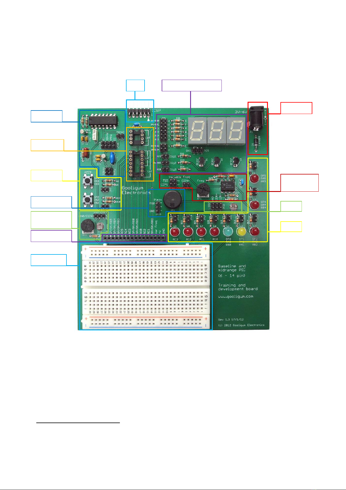
side) via JP21. That is, to use the 32.768 kHz crystal with the PIC’s internal oscillator, you must connect
it through both JP20 and JP21.
The same is true for the 4.00 MHz ceramic resonator. To use it with the PIC’s internal oscillator, connect
one side of the resonator to OSC1 via JP20 and the other side to OSC2 via JP21.
A 10 kΩ resistor and 82 nF capacitor are also provided, and can be connected via JP20 to OSC1, to form
an external RC oscillator with a frequency of around 1 kHz.
The 7-segment LED displays consist of three common-cathode digits, with the anodes of segments A-D,
F and G connected via 330 Ω resistors and jumper block JP4 to pins RA/RB0-1 and RC1-4. Segment E
can be connected via JP5 to either RA/RB2 or RA/RB4.
The common cathode of digit 1 (the digit on the left) can be connected either to ground or a transistor
controlled by RC5, using jumper JP6.
The cathodes of digits 2 and 3 are connected to transistors controlled by RA/RB5 and RC0 respectively.
The base of each of these NPN transistors is connected to its associated PIC pin through a 1 kΩ resistor
and a jumper: JP8 for digit 1, JP9 for digit 2, and JP10 for digit 3. When the PIC pin pulls the base high,
the transistor conducts, shorting the common cathode of the attached digit to ground.
So, to use just a single digit:
Connect segments A-D, F and G to their associated PIC pins, by placing a shunt across every
position in jumper block JP4. That is, you use six shunts at once, in JP4.
Connect segment E to either RA/RB2 or RA/RB4, by placing a shunt in one of the two positions
in jumper block JP5, selecting the PIC pin to be used for segment E.
Connect the common cathode of digit 1 to ground, by placing a shunt across pins 1 and 2 of
jumper JP6.
Leave jumpers JP8, JP9 and JP10 open, so that the transistors will not conduct.
To use multiple digits:
Connect segments A-G to PIC pins using jumper blocks JP4 and JP5, as above.
If you want to use digit 1, connect its common cathode to the transistor controlled by RC5, by
placing a shunt across pins 2 and 3 of JP6.
Connect the transistors controlling whichever digits you wish to use to their associated PIC pins,
using jumpers JP8, JP9 and JP10
For a two-digit display, you would normally use digits 1 and 2, by connecting pins 2 and 3 of JP6, closing
JP8 and JP9, and leaving JP10 open. The two digits would be activated by RC5 and RA/RB5.
But you could instead choose to use digits 2 and 3, by closing JP9 and JP10, and leaving JP6 and JP8
open. The two digits would then be activated by RA/RB5 and RC0.
For a three-digit display, connect pins 2 and 3 of JP6, and close JP8, JP9 and JP10. The three digits are
activated by RC5, RA/RB5 and RC0.
Note that, if you are using multiple digits, you should ensure that only one transistor (and hence digit) is
activated at once.
The variable frequency oscillator, based on a 555 timer, provides a signal with a frequency that can be
varied from approximately 150 Hz to 10 kHz, using trimpot RP1.
The digital form of this signal can be connected to either the Timer 1 gate input, T1G , or the capture
input pin, CCP1, using jumper block JP26.

© Gooligum Electronics 2015 www.gooligum.com.au
Baseline and mid-range PIC training and dev board operation guide Page 7
A sawtooth form of the variable frequency signal can be connected to comparator input C2IN+, via
jumper JP27.
A piezo sounder is connected directly to pin RC5, which is also PWM output P1A.
To drive the piezo using a single-ended PWM output (or by toggling RC5), the other side of the piezo
should be connected to ground, by placing a shunt across positions 1 and 2 of jumper JP23.
Alternatively, the piezo can be driven (at higher volume) by a double-ended or half-bridge PWM output,
by placing a shunt across positions 2 and 3 of JP23, connecting its other side to PWM output P1B.
Finally, every PIC pin, the 32.768 kHz and variable frequency signals and the power supply are brought
out to a 16-pin expansion header, next to the breadboard (making it easy to build custom circuits and to
use this training board a general 6 –14-pin PIC development board), as follows:
Pin
Description
1
32.768 kHz buffered digital signal
2
GP5 / RA5 / RB5
3
GP4 / RA4 / RB4
4
GP3 / RA3 / RB3
5
RC5
6
RC4
7
RC3
8
GP0 / RA0 / RB0
9
GP1 / RA1 / RB1
10
RC0
11
RC2
12
RC1
13
GP2 / RA2 / RB2
14
Variable frequency (150 –10000 Hz) digital signal
15
Power (+V)
16
Ground

© Gooligum Electronics 2015 www.gooligum.com.au
Baseline and mid-range PIC training and dev board operation guide Page 8
Jumper summary
As described above, jumpers are used to configure each function, bringing different elements in or out of
the circuit. Although the function of each jumper is annotated on the PCB overlay, here is a summary of
what each jumper is used for:
Jumper
Position
Function
JP3
-
Enables external pull-up resistor on GP3 / RA3 / RB3 / MCLR
JP4
1
Connects RC3 to LED digits segment D
2
Connects RC4 to LED digits segment C
3
Connects RC2 to LED digits segment B
4
Connects RC1 to LED digits segment A
5
Connects RA1 / RB1 to LED digits segment F
6
Connects RA0 / RB0 to LED digits segment G
JP5
1
Connects RA4 / RB4 to LED digits segment E
2
Connects RA2 / RB2 to LED digits segment E
JP6
1-2
Connects common cathode of LED digit 1 to ground
2-3
Connects common cathode of LED digit 1 to transistor controlled by RC5
JP7
-
Enables external pull-up resistor on GP2 / RA2 / RB2
JP8
-
Connects RC5 to transistor on LED digit 1
JP9
-
Connects RA5 / RB5 to transistor on LED digit 2
JP10
-
Connects RC0 to transistor on LED digit 1
JP11
Connects GP0 / RA0 / RB0 to LED L1
JP12
Connects GP1 / RA1 / RB1 to LED L2
JP13
Connects GP2 / RA2 / RB2 to LED L3
JP14
Connects GP4 / RA4 / RB4 to LED L4
JP15
Connects GP5 / RA5 / RB5 to LED L5
JP16
Connects RC0to LED L6
JP17
Connects RC1 to LED L7
JP18
Connects RC2 to LED L8
JP19
Connects RC3 to LED L9
JP20
1
Connects OSC1 to 10 kΩ resistor and 82 nF capacitor (RC oscillator)
2
Connects OSC1 to 32.768 kHz watch crystal (LP oscillator)
3
Connects OSC1 to 4.00 MHz ceramic resonator (XT oscillator)
4
Connects OSC1 to 32.768 kHz external clock (EC mode)
JP21
1
Connects OSC2 to 4.00 MHz ceramic resonator (XT oscillator)
2
Connects OSC2 to 32.768 kHz watch crystal (LP oscillator)

© Gooligum Electronics 2015 www.gooligum.com.au
Baseline and mid-range PIC training and dev board operation guide Page 9
JP22
-
Connects T0CKI to 32.768 kHz external clock
JP23
1-2
Connects one side of piezo sounder to ground (other side connects to P1A)
2-3
Connects one side of piezo sounder to P1B (other side connects to P1A)
JP24
1-2
Connects 10 kΩ potentiometer to RA0 / CIN+ / C1IN+
2-3
Connects LDR1 to AN0 / CIN+ / C1IN+
JP25
1
Connects LDR2 to AN2
2
Connects LDR2 to C2IN+
3
Connects LDR2 to CIN- / C1IN-
JP26
1
Connects digital variable frequency signal to CCP1
2
Connects digital variable frequency signal to T1G
JP27
-
Connects sawtooth variable frequency signal to C2IN+

© Gooligum Electronics 2015 www.gooligum.com.au
Baseline and mid-range PIC training and dev board operation guide Page 10
Appendix A –Jumper settings
The tables on the following pages show how the jumpers on the training board should be configured, for
each baseline, mid-range or introductory enhanced mid-range tutorial example.
Use a shunt to connect jumpers indicated by ‘●’.
A single digit indicates that you should place a shunt at that numbered position in a jumper block.
‘1-2’ and ‘2-3’ mean that a shunt should be used to connect positions 1 and 2, or 2 and 3, of that jumper.
Jumper block JP4, used to connect PIC pins to six of the 7-segment display anodes, is all or nothing.
Where you see ‘all’, you should place shunts across all six jumpers, numbered 1-6, in the block.
Where a table cell is blank, the jumper should be left open.
In many cases, it won’t matter if additional jumpers are connected, but to ensure that the board is correctly
configured for each lesson, you should leave each jumper unconnected, unless specified.
For example, for mid-range assembler lesson 15, example 6, install shunts on:
JP3 (enabling the pull-up resistor on the pushbutton on RA3)
all positions (1-6) of JP4. connecting pins RA0-1 and RC1-4 to segments A-D and F-G of the 7-
segment displays
position 2 of JP5, connecting pin RA2to segment E of the 7-segment displays
pins 1 and 2 of JP6, connecting the common cathode of digit 1 to ground
position 2 of JP20, connecting one side of a 32.768 kHz watch crystal to OSC1
position 2 of JP21, connecting the other side of the watch crystal to OSC2
Every other jumper should remain open.

© Gooligum Electronics 2015 www.gooligum.com.au
Baseline and mid-range PIC training and dev board operation guide Page 11
Table A-1: Baseline assembler
GP/RA3 pull-up
segment A-D,F,G
segment E
digit 1 cathode
GP/RA2 pull-up
RC5 → digit 1
RA5 → digit 2
RC0 → digit 3
GP/RA0 LED
GP/RA1 LED
GP/RA2 LED
GP/RA4 LED
GP/RA5 LED
RC0 LED
RC1 LED
RC2 LED
RC3 LED
Clock source
Crystal
32 kHz → T0CKI
Piezo
AN0 source
LDR2
Var Freq (digital)
Var Freq (analog)
Lesson
Example
3
4
5
6
7
8
9
10
11
12
13
14
15
16
17
18
19
20
21
22
23
24
25
26
27
1
1
●
2
1
●
3
1
●
2
●
3
●
4
1
●
●
2
●
●
3
●
5
1
●
●
●
2
●
●
●
3
●
●
4
●
●
6
1
●
2
●
●
●
3
●
●
4
●
●
5
●
●
●
●
6
●
7
1
●
●
2
●
●
●
3
●
●
4a
●
4
4b
●
2
2
4c
●
3
1
4d
●
1
8
1
all
1
1-2
2
all
1
2-3
●
●
●
3
all
1
2-3
●
●
●
9
1a
●
1-2
1b
●
2-3
1c
●
2-3
1d
●
2-3
2
●
2-3
3
●
4
●
●
2
5
●
●
2-3
2
10
1
●
●
●
●
1-2
2
all
1
2-3
●
●
1
3
all
1
2-3
●
●
●
11
1
all
1
2-3
●
●
1
2
all
1
2-3
●
●
1

© Gooligum Electronics 2015 www.gooligum.com.au
Baseline and mid-range PIC training and dev board operation guide Page 12
Table A-2: Baseline C
GP/RA3 pull-up
segment A-D,F,G
segment E
digit 1 cathode
GP/RA2 pull-up
RC5 → digit 1
RA5 → digit 2
RC0 → digit 3
GP/RA0 LED
GP/RA1 LED
GP/RA2 LED
GP/RA4 LED
GP/RA5 LED
RC0 LED
RC1 LED
RC2 LED
RC3 LED
Clock source
Crystal
32 kHz → T0CKI
Piezo
AN0 source
LDR2
Var Freq (digital)
Var Freq (analog)
Lesson
Example
3
4
5
6
7
8
9
10
11
12
13
14
15
16
17
18
19
20
21
22
23
24
25
26
27
1
1
●
2
●
3
●
2
1
●
●
2
●
●
3
●
3
1
●
●
●
2
●
●
●
3
●
●
4
●
●
4
1
●
●
2
●
●
●
3
●
●
5
1
all
1
1-2
2
all
1
2-3
●
●
●
6
1a
●
1-2
1b
●
2-3
1c
●
2-3
1d
●
2-3
2
●
2-3
3
●
4
●
●
2
5
●
●
2-3
2
7
1
●
●
●
●
1-2
2
all
1
2-3
●
●
1
3
all
1
2-3
●
●
●
4
all
1
2-3
●
●
1
5
all
1
2-3
●
●
1

© Gooligum Electronics 2015 www.gooligum.com.au
Baseline and mid-range PIC training and dev board operation guide Page 13
Table A-3a: Mid-range assembler (lessons 1 - 8)
GP/RA3 pull-up
segment A-D,F,G
segment E
digit 1 cathode
GP/RA2 pull-up
RC5 → digit 1
RA5 → digit 2
RC0 → digit 3
GP/RA0 LED
GP/RA1 LED
GP/RA2 LED
GP/RA4 LED
GP/RA5 LED
RC0 LED
RC1 LED
RC2 LED
RC3 LED
Clock source
Crystal
32 kHz → T0CKI
Piezo
AN0 source
LDR2
Var Freq (digital)
Var Freq (analog)
Lesson
Example
3
4
5
6
7
8
9
10
11
12
13
14
15
16
17
18
19
20
21
22
23
24
25
26
27
1
1
●
●
2
●
●
2
1
●
●
2
●
●
3
●
●
3
1
●
●
2
●
●
3
●
4
1
●
●
●
2
●
●
●
3
●
●
4
●
●
●
5
1
●
●
2
●
●
●
3
●
●
●
4
●
●
5
●
●
●
●
6
●
●
6
1
●
●
2
●
●
●
3
●
●
4
●
●
●
5
●
●
●
6
●
●
●
●
7
1
●
●
●
2
●
●
●
●
3
●
●
4
●
●
5
●
●
●
6
●
●
8
1
●
2
●
●
4
3
●
●
2
2
4
●
●
3
1
5
●
●
1
6
●
●
●
●

© Gooligum Electronics 2015 www.gooligum.com.au
Baseline and mid-range PIC training and dev board operation guide Page 14
Table A-3b: Mid-range assembler (lessons 9 - 17)
GP/RA3 pull-up
segment A-D,F,G
segment E
digit 1 cathode
GP/RA2 pull-up
RC5 → digit 1
RA5 → digit 2
RC0 → digit 3
GP/RA0 LED
GP/RA1 LED
GP/RA2 LED
GP/RA4 LED
GP/RA5 LED
RC0 LED
RC1 LED
RC2 LED
RC3 LED
Clock source
Crystal
32 kHz → T0CKI
Piezo
AN0 source
LDR2
Var Freq (digital)
Var Freq (analog)
Lesson
Example
3
4
5
6
7
8
9
10
11
12
13
14
15
16
17
18
19
20
21
22
23
24
25
26
27
9
1a
●
●
1-2
1b
●
●
2-3
2
●
●
2-3
3
●
●
2-3
4
●
●
2-3
5
●
●
2-3
6
●
●
●
2-3
7
●
●
●
2-3
3
10
1
●
●
●
●
2
●
3
●
11
1
●
●
●
●
2-3
3
2
●
●
3
3
●
●
2
12
1
all
1
1-2
2
all
1
2-3
●
●
●
3
all
1
2-3
●
●
●
13
1
●
●
●
●
1-2
2
●
●
●
●
1-2
3
all
1
2-3
●
●
●
1
4
all
1
2-3
●
●
●
1
5
all
1
2-3
●
●
●
14
1
all
1
2-3
●
●
1
2
all
1
2-3
●
●
1
15
1
●
●
●
2
●
●
●
3
●
4
4
●
2
2
5
all
2
1-2
2
2
6
●
all
2
1-2
2
2
7
all
2
1-2
2
8
all
2
1-2
●
16
1
●
17
1
all
2
1-2
1
2
all
2
1-2
1
3
all
2
1-2
1
4
●
5
●
6
●
7
all
1
2-3
●
●
1

© Gooligum Electronics 2015 www.gooligum.com.au
Baseline and mid-range PIC training and dev board operation guide Page 15
Table A-3c: Mid-range assembler (lessons 18 - 19)
GP/RA3 pull-up
segment A-D,F,G
segment E
digit 1 cathode
GP/RA2 pull-up
RC5 → digit 1
RA5 → digit 2
RC0 → digit 3
GP/RA0 LED
GP/RA1 LED
GP/RA2 LED
GP/RA4 LED
GP/RA5 LED
RC0 LED
RC1 LED
RC2 LED
RC3 LED
Clock source
Crystal
32 kHz → T0CKI
Piezo
AN0 source
LDR2
Var Freq (digital)
Var Freq (analog)
Lesson
Example
3
4
5
6
7
8
9
10
11
12
13
14
15
16
17
18
19
20
21
22
23
24
25
26
27
18
1
2
1-2
1-2
3
●
1-2
4
1-2
5
2-3
6
1-2
7
1-2
8
1-2
19
1
all
1
2-3
●
●
●
2
all
1
2-3
●
●
●

© Gooligum Electronics 2015 www.gooligum.com.au
Baseline and mid-range PIC training and dev board operation guide Page 16
Table A-4a: Mid-range C (lessons 1 - 6)
GP/RA3 pull-up
segment A-D,F,G
segment E
digit 1 cathode
GP/RA2 pull-up
RC5 → digit 1
RA5 → digit 2
RC0 → digit 3
GP/RA0 LED
GP/RA1 LED
GP/RA2 LED
GP/RA4 LED
GP/RA5 LED
RC0 LED
RC1 LED
RC2 LED
RC3 LED
Clock source
Crystal
32 kHz → T0CKI
Piezo
AN0 source
LDR2
Var Freq (digital)
Var Freq (analog)
Lesson
Example
3
4
5
6
7
8
9
10
11
12
13
14
15
16
17
18
19
20
21
22
23
24
25
26
27
1
1
●
●
2
●
●
3
●
●
4
●
●
5
●
●
6
●
2
1
●
●
●
2
●
●
●
3
●
●
4
●
●
●
3
1
●
●
2
●
●
●
3
●
●
4
●
●
●
5
●
●
●
6
●
●
●
●
4
1
●
●
●
2
●
●
●
●
3
●
●
4
●
●
5
●
●
●
6
●
●
5
1
●
2
●
●
4
3
●
●
2
2
4
●
●
3
1
5
●
●
1
6
●
●
●
●
6
1
●
●
2-3
2
●
●
2-3
3
●
●
2-3
4
●
●
2-3
5
●
●
2-3
6
●
●
●
2-3
7
●
●
●
2-3
3
8
●
●
●
●
2-3
3
9
●
●
3
10
●
●
2

© Gooligum Electronics 2015 www.gooligum.com.au
Baseline and mid-range PIC training and dev board operation guide Page 17
Table A-4b: Mid-range C (lessons 7 - 13)
GP/RA3 pull-up
segment A-D,F,G
segment E
digit 1 cathode
GP/RA2 pull-up
RC5 → digit 1
RA5 → digit 2
RC0 → digit 3
GP/RA0 LED
GP/RA1 LED
GP/RA2 LED
GP/RA4 LED
GP/RA5 LED
RC0 LED
RC1 LED
RC2 LED
RC3 LED
Clock source
Crystal
32 kHz → T0CKI
Piezo
AN0 source
LDR2
Var Freq (digital)
Var Freq (analog)
Lesson
Example
3
4
5
6
7
8
9
10
11
12
13
14
15
16
17
18
19
20
21
22
23
24
25
26
27
7
1
all
1
1-2
2
all
1
2-3
●
●
●
8
1
●
●
●
●
1-2
2
●
●
●
●
1-2
3
all
1
2-3
●
●
●
1
4
all
1
2-3
●
●
●
1
5
all
1
2-3
●
●
●
6
all
1
2-3
●
●
1
7
all
1
2-3
●
●
1
9
1
●
●
●
2
●
●
●
3
●
2
2
4
all
2
1-2
2
2
5
●
all
2
1-2
2
2
6
all
2
1-2
2
7
all
2
1-2
●
10
1
●
11
1
all
2
1-2
1
2
all
2
1-2
1
3
all
2
1-2
1
4
●
5
●
6
●
7
all
1
2-3
●
●
1
12
1
2
1-2
1-2
3
●
1-2
4
1-2
5
2-3
6
1-2
7
1-2
8
1-2
13
1
all
1
2-3
●
●
●
2
all
1
2-3
●
●
●
3
all
1
2-3
●
●
●

© Gooligum Electronics 2015 www.gooligum.com.au
Baseline and mid-range PIC training and dev board operation guide Page 18
Table A-5: Migrating to enhanced mid-range assembler
GP/RA3 pull-up
segment A-D,F,G
segment E
digit 1 cathode
GP/RA2 pull-up
RC5 → digit 1
RA5 → digit 2
RC0 → digit 3
GP/RA0 LED
GP/RA1 LED
GP/RA2 LED
GP/RA4 LED
GP/RA5 LED
RC0 LED
RC1 LED
RC2 LED
RC3 LED
Clock source
Crystal
32 kHz → T0CKI
Piezo
AN0 source
LDR2
Var Freq (digital)
Var Freq (analog)
Lesson
Example
3
4
5
6
7
8
9
10
11
12
13
14
15
16
17
18
19
20
21
22
23
24
25
26
27
1
1
●
●
2
●
●
3
●
●
4
●
●
5
●
●
6
●
2
1
●
●
●
2
●
●
3
●
●
●
4
●
●
3
1
●
●
2
●
●
●
3
●
●
4
●
●
5
●
●
6
●
4
1
●
●
2
●
3
1
3
●
1
4
●
1
5
●
●
●
●
5
1a
●
1-2
1b
●
1-2
1c
●
2-3
1d
●
2-3
2
●
3
3
●
3
4
●
3
5
●
3
6
7
●
●
3
6
1
all
1
1-2
7
1
●
●
●
●
1-2
2
all
1
2-3
●
●
●
8
1
all
1
2-3
●
●
1
2
all
1
2-3
●
●
1
9
1
all
2
1-2
2
2
all
2
1-2
2
3
all
2
1-2
10
1
●
11
1
●
2
●
1-2
3
2-3

© Gooligum Electronics 2015 www.gooligum.com.au
Baseline and mid-range PIC training and dev board operation guide Page 19
Table A-6: Migrating to enhanced mid-range C
GP/RA3 pull-up
segment A-D,F,G
segment E
digit 1 cathode
GP/RA2 pull-up
RC5 → digit 1
RA5 → digit 2
RC0 → digit 3
GP/RA0 LED
GP/RA1 LED
GP/RA2 LED
GP/RA4 LED
GP/RA5 LED
RC0 LED
RC1 LED
RC2 LED
RC3 LED
Clock source
Crystal
32 kHz → T0CKI
Piezo
AN0 source
LDR2
Var Freq (digital)
Var Freq (analog)
Lesson
Example
3
4
5
6
7
8
9
10
11
12
13
14
15
16
17
18
19
20
21
22
23
24
25
26
27
1
1
●
●
2
●
●
3
●
●
4
●
2
1
●
●
●
2
●
●
3
●
●
●
4
●
●
3
1
●
●
2
●
●
●
3
●
●
4
●
●
5
●
●
6
●
4
1
●
●
2
●
3
1
3
●
1
4
●
1
5
●
●
●
●
5
1a
●
1-2
1b
●
1-2
1c
●
2-3
1d
●
2-3
2
●
3
3
●
3
4
●
3
5
●
3
6
7
●
●
3
6
1
●
●
●
●
1-2
2
all
1
2-3
●
●
●
3
all
1
2-3
●
●
1
7
1
all
2
1-2
2
2
all
2
1-2
2
3
all
2
1-2
8
1
●
9
1
●
2
●
1-2
3
2-3

© Gooligum Electronics 2015 www.gooligum.com.au
Baseline and mid-range PIC training and dev board operation guide Page 20
Table A-7a: Enhanced mid-range assembler (lessons 1 - 10)
GP/RA3 pull-up
segment A-D,F,G
segment E
digit 1 cathode
GP/RA2 pull-up
RC5 → digit 1
RA5 → digit 2
RC0 → digit 3
GP/RA0 LED
GP/RA1 LED
GP/RA2 LED
GP/RA4 LED
GP/RA5 LED
RC0 LED
RC1 LED
RC2 LED
RC3 LED
Clock source
Crystal
32 kHz → T0CKI
Piezo
AN0 source
LDR2
Var Freq (digital)
Var Freq (analog)
Lesson
Example
3
4
5
6
7
8
9
10
11
12
13
14
15
16
17
18
19
20
21
22
23
24
25
26
27
1
1
●
2
1
●
3
1
●
2
●
4
1
●
●
2
●
●
3
●
5
1
●
●
●
2
●
●
●
3
●
●
4
●
●
6
1
●
2
●
●
●
3
●
●
4
●
●
5
●
●
●
●
6
●
7a
●
●
7b
●
7
1
●
2
●
●
●
3
●
●
4
●
●
●
5
●
●
6
●
●
●
8
1
●
●
2
●
●
●
3
●
●
4
●
●
5
●
●
6
●
9
1
●
●
2
●
4
3
●
2
2
4
●
3
1
5
●
1
6
●
1
7
●
●
●
●
10
1a
●
1-2
1b
●
1-2
1c
●
2-3
1d
●
2-3
2
●
3
3
●
3
4
●
3
Table of contents