HARTMANN ELECTRONIC BUS908 Instructions for use

Hartmann Electronic GmbH Backplanes
Motorstraße 43 Aufbausysteme (MPS)
Tel.: +49 711 1 39 89-0 Layoutservice
Fax: +49 711 8 66 11 91
www.hartmann-electronic.com
Geschäftsführer: Registergericht Stgt. HRB 7630 Deutsche Bank AG, Singen
Werner Fritz USt.-Id.-Nr. DE 147816208 BLZ 692 700 38 - Kto.-Nr. 050 1403 00
Dr. Günter Zahnenbenz Steuer-Nr. 9908300985 Swift-Code DEUTDE6F692
1
Hardware User Manual,
CPCI Rear Board - PCIeX1 to 8CPCI-Slot
BUS908

Hartmann Electronic GmbH Backplanes
Motorstraße 43 Aufbausysteme (MPS)
Tel.: +49 711 1 39 89-0 Layoutservice
Fax: +49 711 8 66 11 91
www.hartmann-electronic.com
Geschäftsführer: Registergericht Stgt. HRB 7630 Deutsche Bank AG, Singen
Werner Fritz USt.-Id.-Nr. DE 147816208 BLZ 692 700 38 - Kto.-Nr. 050 1403 00
Dr. Günter Zahnenbenz Steuer-Nr. 9908300985 Swift-Code DEUTDE6F692
2
HUM Rev: Notification of Change Date (Revision) Author
R 1.0 -Ordering Information 24.12.2014 J. Brosowski
Impressum:
Hartmann Electronic GmbH
Motorstraße 43, D-70499 Stuttgart (Weilimdorf)
Telefon + 49 711 1 39 89-0
Telefax + 49 711 8 66 11 91
E-mail info @ hartmann-elektronik.de
Internet www.hartmann-electronic.com
Hartmann Elektronik is a longstanding partner of the
embedded industry and has a variety of different backplanes.
With our wide selection of backplanes and enclosure you can
build your perfect system platform
Copyright © 2014
All rights and technical modifications reserved

Hartmann Electronic GmbH Backplanes
Motorstraße 43 Aufbausysteme (MPS)
Tel.: +49 711 1 39 89-0 Layoutservice
Fax: +49 711 8 66 11 91
www.hartmann-electronic.com
Geschäftsführer: Registergericht Stgt. HRB 7630 Deutsche Bank AG, Singen
Werner Fritz USt.-Id.-Nr. DE 147816208 BLZ 692 700 38 - Kto.-Nr. 050 1403 00
Dr. Günter Zahnenbenz Steuer-Nr. 9908300985 Swift-Code DEUTDE6F692
3
Table of Contents
1. Overview................................................................................................................................................................4
1.1 Block Diagram .................................................................................................................................................5
1.2 Specifications ..................................................................................................................................................6
2. Switch Settings ......................................................................................................................................................7
3. Initial Set-Up ........................................................................................................................................................11
3.1 Installing the board into a CPCI system........................................................................................................11
3.2 Installing a third party PCIe device at the PCIe X1 Downstream Port ..........................................................11
4. LED Description...................................................................................................................................................12
5. Pin Assignments ..................................................................................................................................................14
6. CE Compliance....................................................................................................................................................17
7. Ordering Information............................................................................................................................................18

Hartmann Electronic GmbH Backplanes
Motorstraße 43 Aufbausysteme (MPS)
Tel.: +49 711 1 39 89-0 Layoutservice
Fax: +49 711 8 66 11 91
www.hartmann-electronic.com
Geschäftsführer: Registergericht Stgt. HRB 7630 Deutsche Bank AG, Singen
Werner Fritz USt.-Id.-Nr. DE 147816208 BLZ 692 700 38 - Kto.-Nr. 050 1403 00
Dr. Günter Zahnenbenz Steuer-Nr. 9908300985 Swift-Code DEUTDE6F692
4
1. Overview
This manual describes the CPCI Rear board - PCIeX1 to 8CPCI-Slot. This board enables the operation of a CPCI
System through a normal desktop PC. Therefore, a PCIe to PCIe Cable slot card (see picture below) can be
plugged into the desktop PC. The CPCI board can be linked through a PCIe X1 Cable with this adapter board
and therefore with the desktop PC.
Figure 1: PCIe to PCIe X1 Cable lot card
The CPCI board is designed as a CPCI System Slot board. It has to be plugged into the System Slot of a 3U, 32
bit CPCI Backplane. The number of supported slots at the backplane is limited to max. 8 slot. In accordance with
the CPCI specification1the following number of slots at the backplane are supported:
VI/O PCI - Clock
Frequency # Slots
+3.3V 66MHz ≤5 Slots
+3.3V 33MHz up to 8 Slots
+5V 33MHz up to 8 Slots
Table 1: number of supported slots at the backplane
The board is designed to support a 33MHz or 66MHz clock. The selection of the clock frequency is executed by
the backplane (“M66EN” Pin). Despite that the Add-In Card is PXI compliant.
With the PCIe X1 Cable Downstream port, it is possible to cascade several CPCI Boards to operate several CPCI
Systems.
There are no additional software-drivers required to operate this board.
1PICMG 2.0 R3.0 CompactPCI®Specification

Hartmann Electronic GmbH Backplanes
Motorstraße 43 Aufbausysteme (MPS)
Tel.: +49 711 1 39 89-0 Layoutservice
Fax: +49 711 8 66 11 91
www.hartmann-electronic.com
Geschäftsführer: Registergericht Stgt. HRB 7630 Deutsche Bank AG, Singen
Werner Fritz USt.-Id.-Nr. DE 147816208 BLZ 692 700 38 - Kto.-Nr. 050 1403 00
Dr. Günter Zahnenbenz Steuer-Nr. 9908300985 Swift-Code DEUTDE6F692
5
1.1 Block Diagram
Figure 2: Block Diagram

Hartmann Electronic GmbH Backplanes
Motorstraße 43 Aufbausysteme (MPS)
Tel.: +49 711 1 39 89-0 Layoutservice
Fax: +49 711 8 66 11 91
www.hartmann-electronic.com
Geschäftsführer: Registergericht Stgt. HRB 7630 Deutsche Bank AG, Singen
Werner Fritz USt.-Id.-Nr. DE 147816208 BLZ 692 700 38 - Kto.-Nr. 050 1403 00
Dr. Günter Zahnenbenz Steuer-Nr. 9908300985 Swift-Code DEUTDE6F692
6
1.2 Specifications
Typical Power Consumption:
Minimum Input Voltage: +3.15V at supervisory circuit @ 3.3V. Else: Fundamental Reset is
asserted (LED “RES” and all other Resets). Voltage drop at Backplane,
Power input, and Board is not included.
Form Factor: Eurocard (80x100mm); suitable for 19“-Racks. Front panel width
4HP (20.32mm).
Front Panel Connector: 2 times PCIe-X1-Cable-Connector (PCI Express®External
Cabling Specification Revision 2.0)
PCIe Specification: PCI Express®Card Electromechanical Specification Revision 2.0
PCI Express®Base Specification Revision 1.0a
CPCI System Slot: PICMG 2.0 R3.0 CompactPCI®Specification
Operating Temperature Range: -20°C - +85°C
Required voltages at CPCI-Backplane: +3,3V & +VIO. The +VIO-Voltage can be either +3,3V or +5V.
Voltage Supervisory: A Voltage Supervisory circuit is implemented at the board.
Following Voltages are supervised:
+1V0 Switch (VDDA, VDDC)
+1.5V Switch (VTT)
+3V3
1,8V Bridge (VDDA, VDDC,…)
1,8V Clock
Power Supplies: Liner regulators: 5 times +1,8V
Linerregulator:+1.5V
DC/DC Power Module: 2 times +1V0
Typical Power
Consumption Voltage Current Power Total Power
VIO = +3,3V +3,3V 900mA ≈3W 3W
+5V 0A 0W
VIO = +5V +3,3V 900mA ≈3W 3W
+5V 0.05A max

Hartmann Electronic GmbH Backplanes
Motorstraße 43 Aufbausysteme (MPS)
Tel.: +49 711 1 39 89-0 Layoutservice
Fax: +49 711 8 66 11 91
www.hartmann-electronic.com
Geschäftsführer: Registergericht Stgt. HRB 7630 Deutsche Bank AG, Singen
Werner Fritz USt.-Id.-Nr. DE 147816208 BLZ 692 700 38 - Kto.-Nr. 050 1403 00
Dr. Günter Zahnenbenz Steuer-Nr. 9908300985 Swift-Code DEUTDE6F692
7
2. Switch Settings
Please configure Dip Switches before use.
The default setup of the Dip Switches is as follows:
The Dip Switch name is labeled at PCB.
The board should run correctly with the default setup. The default setup of the Dip Switches is marked
green.
To optimize the signal integrity of the board in special system environments the following DIP switches can be
adjusted: SWTRM, SWDEQ, SWDRV and SWDTX. These Dip Switches configure physical layer properties of
the switch.
Figure 3: Dip-Switches labeled on PCB.
SWCLK (Advanced Use)
The PCIe Switch and the PCIe to PCI Bridge can be configured via I2C / SMBUS or EEPROM Position “3”
determines if the PCIe to PCI Bridge can be configured via SMBUS (OFF) or via EEPROM. Turn Position “4”
“OFF” to configure the EEPROM of the Bridge or “ON” to configure EEPROM of the Switch.
SWCLK
PIN OFF ON
1 No Function No Function
2 No Function No Function
3 Bridge in SMBUS-Mode Bridge in EEPROM-Mode
4 I2C(XDEV) to Bridge+EEPROM I2C(XDEV) to EEPROM of Switch
Table 2: Setup of Dip Switch SWCLK. Default setup is marked green.

Hartmann Electronic GmbH Backplanes
Motorstraße 43 Aufbausysteme (MPS)
Tel.: +49 711 1 39 89-0 Layoutservice
Fax: +49 711 8 66 11 91
www.hartmann-electronic.com
Geschäftsführer: Registergericht Stgt. HRB 7630 Deutsche Bank AG, Singen
Werner Fritz USt.-Id.-Nr. DE 147816208 BLZ 692 700 38 - Kto.-Nr. 050 1403 00
Dr. Günter Zahnenbenz Steuer-Nr. 9908300985 Swift-Code DEUTDE6F692
8
SWSMB (Advanced Use)
The DIP Switch can be used to select the SMBUS-Address of the Switch. Turn DIP-SWITCH (only positions “2”,
“3”,” “4) “ON” to ground the first bits on the SMBUS address as follows.
Figure 4: Selection of SMBUS Address
If SMBUS is not activated Pins can be used as GPIOs.
Turn all positions “OFF” if feature is not used.
SWSMB
PIN OFF ON
1 SW_GPIO4 SW_GPIO4
2 SW_GPIO7; SMB-ADDR Bit2 SW_GPIO7 , SMB-ADDR Bit2
3 SW_GPIO6; SMB-ADDR Bit1 SW_GPIO6, SMB-ADDR Bit1
4 SW_GPIO5, SMB-ADDR Bit0 SW_GPIO4, SMB-ADDR Bit0
Table 3: Setup of Dip Switch SWSMB. Default setup is marked green.
SWTRM (Signal integrity optimization)
Receiver Termination Adjustment (Positions “1”;” 2”): The Termination Resistor value of each receiver
differential pair of the switch can be adjusted as shown in the table below to improve signal integrity.
Transmitter Termination Adjustment (Positions “3”; “4”): The Termination Resistor value of each transmitter
differential pair of the switch can be adjusted as shown in the table below to improve signal integrity.
SWTRM
PIN OFF= LOW =Default/ ON = HIGH Value
1 Bit0(L) - RXTRMADJ0 RX Termination Adjust
RXTRMADJ0[1:0]
2 Bit1(L) - RXTRMADJ1 00=52 ,01=57,10=43, 11=46 [Ohm]
3 Bit0(L) - TXTRMADJ0
TX Termination Adjust
TXRMADJ0[1:0]
4 Bit1(L) - TXTRMADJ1 00=52, 01=57 ,10=43, 11=46 [Ohm]
Table 4: Setup of Dip Switch SWTRM. Default setup is marked green.

Hartmann Electronic GmbH Backplanes
Motorstraße 43 Aufbausysteme (MPS)
Tel.: +49 711 1 39 89-0 Layoutservice
Fax: +49 711 8 66 11 91
www.hartmann-electronic.com
Geschäftsführer: Registergericht Stgt. HRB 7630 Deutsche Bank AG, Singen
Werner Fritz USt.-Id.-Nr. DE 147816208 BLZ 692 700 38 - Kto.-Nr. 050 1403 00
Dr. Günter Zahnenbenz Steuer-Nr. 9908300985 Swift-Code DEUTDE6F692
9
SWDEQ (Signal integrity optimization)
The equalization function of transmitting channels can optimize the driver current for different cable lengths and
materials. The table shown below lists the combinations of de-emphasized driver current (ITX –IEQ) to non-de-
emphasized driver current (ITX) for different values of “DEQ[3:0]”.
Table 5: Status of the signals “DEQ[3:0]” related to the needed deemphasis
Recommended De-emphasis settings for different PCIe-X1 Cable lengths at the Upstream Port:
2m: -1.51 dB
7m: -3.88 dB
SWDEQ
PIN Pin Function Value
1 Bit0(L = OFF, H =ON) DEQ0 De-emphasis for different PCIe X1 Cable lengths
at the upstream port
2 Bit1(L = OFF, H= ON) - DEQ1
DEQ[3:0]
0100 = -1.51dB
1001 = -3.88dB
3 Bit2(L = OFF, H = ON) - DEQ2
4 Bit3(H = OFF, L = ON) - DEQ3
Table 6: Setup of Dip Switch SWDEQ. Default setup is marked green.
Note: The De-emphasis is calculated for the case that two CPCI Rear boards are cascaded (Upstream- and
Downstream-Port linked) through a PCIe X1 Cable. The De-emphasis can be optimized for adapter
boards with higher or lower insertion loss differences.

Hartmann Electronic GmbH Backplanes
Motorstraße 43 Aufbausysteme (MPS)
Tel.: +49 711 1 39 89-0 Layoutservice
Fax: +49 711 8 66 11 91
www.hartmann-electronic.com
Geschäftsführer: Registergericht Stgt. HRB 7630 Deutsche Bank AG, Singen
Werner Fritz USt.-Id.-Nr. DE 147816208 BLZ 692 700 38 - Kto.-Nr. 050 1403 00
Dr. Günter Zahnenbenz Steuer-Nr. 9908300985 Swift-Code DEUTDE6F692
10
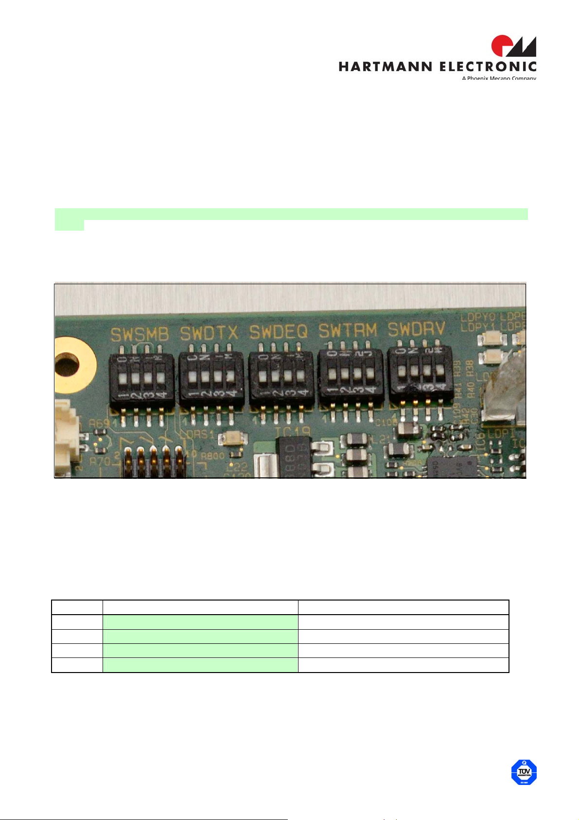
SWDRV SWDTX (Signal integrity optimization)
“LODRV”, “HIDRV”, “DTX[0:3]”
In order to meet the different application needs, the driving current and equalization of each transmitting channels
can be adjusted using Dip Switches .The driver current of each channel is set to 20mA in default mode. To
change the current value, the user can strap
the pins either for nominal value (“HIDRV”, “LODRV”) or actual value (“DTX [3:0]”), which is a scaled multiple of
Inom. The following tables illustrate the possible transmitted current values the switch provides.
“RXEQCTL[1:0]”
In order to improve the data stream integrity across the channels, the receiver of each port of the Switch includes
a reception equalizer to mitigate the effects of ISI. The reception equalizer is implemented as a selectable high-
pass filter at the input node, and it is capable of removing as much as 0.4UI of ISI related jitter. The following
table shows a simple guideline for selecting the appropriate value to adapt with different lengths or connector
numbers in various applications.
Figure 5: Adjustment of „RXEQTL[1:0“]
SWDRV
PIN OFF=Default/ON Value
1-8 Bit0(L = OFF) - LODRV Nominal Driver Current
2-7 Bit1(L = OFF) - HIDRV 00=20mA,01=10mA,10=28mA
3-6 Bit0(L = OFF) - RXEQCTL0 RX Equalizer Settings
4-5 Bit1(L = OFF) - RXEQCTL1
00=Jitter>0.25UI,Len>20",CON>=2,
01=Jitter>0.1UI<0.25UI,Len=8"-20",CON<=2,
1X=Jitter<0.1UI,Len<=8",CON<=1
Table 7: Setup of Dip Switch SWDRV. Default setup is marked green.
SWDTX
PIN OFF=Default/ON Value
1-8 Bit0(L = OFF) - DTX0 Multiple Nominal Driver Current
2-7 Bit1(L = OFF) - DTX1 DTX[3:0]
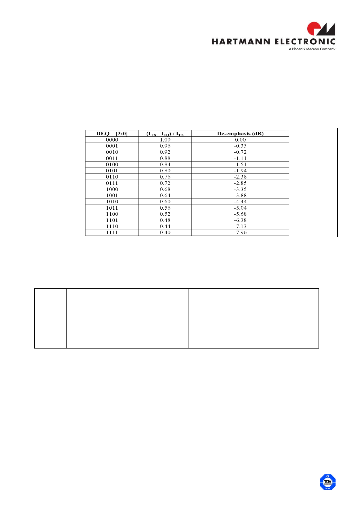
0000-0111 = 1.00-1.35 (+0.05)
3-6 Bit2(L = OFF) - DTX2 1000-1111 = 0.60-0.95 (+0.05)
4-5 Bit3(L = OFF) - DTX3
Table 8: Setup of Dip Switch SWDTX. Default setup is marked green.

Hartmann Electronic GmbH Backplanes
Motorstraße 43 Aufbausysteme (MPS)
Tel.: +49 711 1 39 89-0 Layoutservice
Fax: +49 711 8 66 11 91
www.hartmann-electronic.com
Geschäftsführer: Registergericht Stgt. HRB 7630 Deutsche Bank AG, Singen
Werner Fritz USt.-Id.-Nr. DE 147816208 BLZ 692 700 38 - Kto.-Nr. 050 1403 00
Dr. Günter Zahnenbenz Steuer-Nr. 9908300985 Swift-Code DEUTDE6F692
11
3. Initial Set-Up
3.1 Installing the board into a CPCI system
1) Power down your host system and your external CPCI System.
2) Insert the CPCI Board into the System Slot of your CPCI system. Make sure that the latch of the CPCI board is
closed.
3) Connect your host system through a PCIe X1 Cable to the upstream port of the CPCI board.
4) Tighten the screws of the X1 Cable at the host (or host adapter) and the board.
5.) Before applying power to your external CPCI system make sure that all other CPCI
Boards are installed correctly in your system. You may follow the instruction of your
CPCI board supplier to install the board mechanically.
6) Power up your external CPCI system.
7) Power up your host system.
8) Your CPCI system should be enumerated automatically.
3.2 Installing a third party PCIe device at the PCIe X1 Downstream Port
1) Power down your host system and your second and third party CPCI system.
Second party system: System that is connected directly to the host system.
Third party system: System that is connected to the host through the second party system.
2) Insert the CPCI Board into the system slot of your second party CPCI system.
Make sure that the latch of the CPCI board is closed.
3) Connect your host system through a PCIe X1 Cable to the upstream port of the board that is plugged into your
second party system.
4) Tighten the screws of the PCIe X1 Cable at the host (or host adapter) and the board of the second party
system.
5) Insert the CPCI Board into the system slot of your third party CPCI system.
Make sure that the latch of the CPCI board is closed.
6) Connect the downstream port of the second party system board with the upstream port of the third party
system board via a PCIe X1 Cable.
7) Tighten the screws of the X1 Cable on both boards (second party board and third party board).
8) Power up your third party CPCI system
9) Power up your second party CPCI system
10) Power up your host system
11) Both of your CPCI systems should be enumerated automatically
Note: The system that is at the lowest level of the hierarchical PCIe structure should
be powered up first.

Hartmann Electronic GmbH Backplanes
Motorstraße 43 Aufbausysteme (MPS)
Tel.: +49 711 1 39 89-0 Layoutservice
Fax: +49 711 8 66 11 91
www.hartmann-electronic.com
Geschäftsführer: Registergericht Stgt. HRB 7630 Deutsche Bank AG, Singen
Werner Fritz USt.-Id.-Nr. DE 147816208 BLZ 692 700 38 - Kto.-Nr. 050 1403 00
Dr. Günter Zahnenbenz Steuer-Nr. 9908300985 Swift-Code DEUTDE6F692
12
4. LED Description
LEDs at Front Panel:
1 “POW” :Green: Power OK (1,8V). “LDPI”
2 “RES” : :Red: Fundamental-Reset is asserted. “LDRS”
3 “RESP” :Red: Reset of the PCI bus is asserted. “LDRSP
4 “POW2” :Green: power at X1 Downstream Port OK. “LDPI2”
5 “RES2” :Red: Reset to Downstream Port active “LDRS2”
6 “PHY2” :Flashing orange: Error is detected at X1 Cable downstream port “LDPY2”
Figure 6: LED Position Front Panel, LED Placement Layout

Hartmann Electronic GmbH Backplanes
Motorstraße 43 Aufbausysteme (MPS)
Tel.: +49 711 1 39 89-0 Layoutservice
Fax: +49 711 8 66 11 91
www.hartmann-electronic.com
Geschäftsführer: Registergericht Stgt. HRB 7630 Deutsche Bank AG, Singen
Werner Fritz USt.-Id.-Nr. DE 147816208 BLZ 692 700 38 - Kto.-Nr. 050 1403 00
Dr. Günter Zahnenbenz Steuer-Nr. 9908300985 Swift-Code DEUTDE6F692
13
Internal LEDs:
LDPY0 (orange) Data error at the Upstream Port of the
Switch (X1 Cable Upstream Port).
Orange when error detected
LDPY0 (orange) Data error at the Downstream Port of the
Switch (Port that is linked to the PCIe to
PCI Bridge). Orange when error detected
LDRS1 (red) Resets the PCIe to PCI Bridge. Red
when asserted
Figure 7: Placement internal LEDs

Hartmann Electronic GmbH Backplanes
Motorstraße 43 Aufbausysteme (MPS)
Tel.: +49 711 1 39 89-0 Layoutservice
Fax: +49 711 8 66 11 91
www.hartmann-electronic.com
Geschäftsführer: Registergericht Stgt. HRB 7630 Deutsche Bank AG, Singen
Werner Fritz USt.-Id.-Nr. DE 147816208 BLZ 692 700 38 - Kto.-Nr. 050 1403 00
Dr. Günter Zahnenbenz Steuer-Nr. 9908300985 Swift-Code DEUTDE6F692
14
5. Pin Assignments
CPCI System Slot 32 Bit:
22 GND GA4 GA3 GA2 GA1 GA0 GND
21 GND CLK6 GND BP(I/O) BP(I/O) BP(I/O) GND
20 GND CLK5 GND BP(I/O) BP(I/O) BP(I/O) GND
19 GND BP(I/O) BP(I/O) BP(I/O) BP(I/O) BP(I/O) GND P2
18 GND BP(I/O) BP(I/O) BP(I/O) BP(I/O) BP(I/O) GND
/
17 GND BP(I/O) BP(I/O) BP(I/O) REQ6# GNT6#
GND J2
16 GND BP(I/O) BP(I/O) BP(I/O) BP(I/O) BP(I/O) GND
15 GND BP(I/O) BP(I/O) BP(I/O) REQ5# GNT5# GND
14 GND BP(I/O) BP(I/O) BP(I/O) BP(I/O) BP(I/O) GND
13 GND BP(I/O) BP(I/O) BP(I/O) BP(I/O) BP(I/O) GND
12 GND BP(I/O) BP(I/O) BP(I/O) BP(I/O) BP(I/O) GND
11 GND BP(I/O) BP(I/O) BP(I/O) BP(I/O) BP(I/O) GND
10 GND BP(I/O) BP(I/O) BP(I/O) BP(I/O) BP(I/O) GND C
9 GND BP(I/O) BP(I/O) BP(I/O) BP(I/O) BP(I/O) GND O
8 GND BP(I/O) BP(I/O) BP(I/O) BP(I/O) BP(I/O) GND N
7 GND BP(I/O) BP(I/O) BP(I/O) BP(I/O) BP(I/O) GND N
6 GND BP(I/O) BP(I/O) BP(I/O) BP(I/O) BP(I/O) GND E
5 GND BP(I/O) BP(I/O) BP(I/O) BP(I/O) BP(I/O) GND C
4 GND BP(I/O) BP(I/O) BP(I/O) BP(I/O) BP(I/O) GND T
3 GND CLK4 GND GNT3# REQ4# GNT4# GND O
2 GND CLK2 CLK3 SYSEN# GNT2# REQ3# GND R
1 GND CLK1 GND REQ1# GNT1# REQ2# GND
25 GND 5V REQ64# ENUM# 3.3V 5V GND
24 GND AD[1] 5V V(I/O) AD[0] ACK64# GND
23 GND 3.3V AD[4] AD[3] 5V AD[2] GND
22 GND AD[7] GND 3.3V AD[6] AD[5] GND P1
21 GND 3.3V AD[9] AD[8] M66EN C/BE[0]# GND
/
20 GND AD[12] GND V(I/O) AD[11] AD[10] GND J1
19 GND 3.3V AD[15] AD[14] GND AD[13] GND
18 GND SERR# GND 3.3V PAR C/BE[1]# GND
17 GND 3.3V IPMB SCL IPMB SDA GND PERR# GND
16 GND DEVSEL# GND V(I/O) STOP# LOCK# GND C
15 GND 3.3V FRAME# IRDY# GND TRDY# GND O
12-14 KEY AREA N
11 GND AD[18] AD[17] AD[16] GND C/BE[2]# GND N
10 GND AD[21] GND 3.3V AD[20] AD[19] GND E
9 GND C/BE[3]# GND AD[23] GND AD[22] GND C
8 GND AD[26] GND V(I/O) AD[25] AD[24] GND T
7 GND AD[30] AD[29] AD[28] GND AD[27] GND O
6 GND REQ0# GND 3.3V CLK0 AD[31] GND R
5 GND BRSVP1A5 BRSVP1B5 RST# GND GNT0# GND
4 GND IPMB PWR HEALTHY# V(I/O) INTP INTS GND
3 GND INTA# INTB# INTC# 5V INTD# GND
2 GND TCK 5V TMS TDO TDI GND
1 GND 5V -12V TRST# 12V 5V GND
Pin Z A B C D E F
length of pins (front view)
short medium long

Hartmann Electronic GmbH Backplanes
Motorstraße 43 Aufbausysteme (MPS)
Tel.: +49 711 1 39 89-0 Layoutservice
Fax: +49 711 8 66 11 91
www.hartmann-electronic.com
Geschäftsführer: Registergericht Stgt. HRB 7630 Deutsche Bank AG, Singen
Werner Fritz USt.-Id.-Nr. DE 147816208 BLZ 692 700 38 - Kto.-Nr. 050 1403 00
Dr. Günter Zahnenbenz Steuer-Nr. 9908300985 Swift-Code DEUTDE6F692
15
PCIe X1 Cable Connector Upstream & Downstream:
PCI Express®External Cabling Specification Revision 2.0
Figure 8: Pin Assingment X1 Cable Connector
Pin Signal Signal Pin
A1 PERn0 GND B1
A2 PERp0 n.c. B2
A3 n.c. CWAKE# B3
A4 SB_RTN CPRSNT# B4
A5 CREFCLKn GND B5
A6 CREFCLKp PWR B6
A7 PWR_RTN CPWRON B7
A8 CPERST# PETn0 B8
A9 GND PETp0 B9
B1
A
1

Hartmann Electronic GmbH Backplanes
Motorstraße 43 Aufbausysteme (MPS)
Tel.: +49 711 1 39 89-0 Layoutservice
Fax: +49 711 8 66 11 91
www.hartmann-electronic.com
Geschäftsführer: Registergericht Stgt. HRB 7630 Deutsche Bank AG, Singen
Werner Fritz USt.-Id.-Nr. DE 147816208 BLZ 692 700 38 - Kto.-Nr. 050 1403 00
Dr. Günter Zahnenbenz Steuer-Nr. 9908300985 Swift-Code DEUTDE6F692
16
Other Connectors:
XJTGB is linked to the PCIe to PCI Bridge.
XJTGS is linked to the PCIe Switch.
XDEVS is linked to the “GPIO[0:7]” Pins of the PCIe Switch.
XDEV is linked to the “GPIO[0:3]” Pins of the PCIe to PCI Bridge The SMBUS on the board is accessible through
XDEV. The position 4 of the Dip Switch “SWCLK” determines if the SMBUS is connected to the PCIe to PCI
Bridge or to the PCIe Switch.
Figure 9: Pin Assignments of XJTGB, XJTGS, XDEVS, XDEV

Hartmann Electronic GmbH Backplanes
Motorstraße 43 Aufbausysteme (MPS)
Tel.: +49 711 1 39 89-0 Layoutservice
Fax: +49 711 8 66 11 91
www.hartmann-electronic.com
Geschäftsführer: Registergericht Stgt. HRB 7630 Deutsche Bank AG, Singen
Werner Fritz USt.-Id.-Nr. DE 147816208 BLZ 692 700 38 - Kto.-Nr. 050 1403 00
Dr. Günter Zahnenbenz Steuer-Nr. 9908300985 Swift-Code DEUTDE6F692
17
6. CE Compliance
The Board is CE-Compliant.
Figure 10: Measurement with data traffic. Radio frequency Disturbance EN55022B

Hartmann Electronic GmbH Backplanes
Motorstraße 43 Aufbausysteme (MPS)
Tel.: +49 711 1 39 89-0 Layoutservice
Fax: +49 711 8 66 11 91
www.hartmann-electronic.com
Geschäftsführer: Registergericht Stgt. HRB 7630 Deutsche Bank AG, Singen
Werner Fritz USt.-Id.-Nr. DE 147816208 BLZ 692 700 38 - Kto.-Nr. 050 1403 00
Dr. Günter Zahnenbenz Steuer-Nr. 9908300985 Swift-Code DEUTDE6F692
18
7. Ordering Information
CPCI System Slot Rear Board - PCIeX1 to 8CPCI-Slot (BUS908)
Order Number Variante VIO
1H00004630 Var1 +3.3V
1H00004640 Var2 +5V
CPCI System Slot Board – PCIeX1 to 8CPCI-Slot (BUS907)
Order Number Variante VIO ECO Front
Panel
1H00005050 Var1 +3.3V No Yes
1H00005060 Var2 +5V No Yes
1H00005070 Var3 +3.3V Yes No
1H00005080 Var4 +5V No No
PCIe X1 Cable
Order Number Length
F0006.02000 0.5m
F0006.02010 1m
F0006.02020 2m
F0006.02040 4m
F0006.02070 7m
Table of contents
Popular Computer Hardware manuals by other brands

ekwb
ekwb EK-XRES DCP 4.0 INSTALLATION AND MOUNTING MANUAL

Cypress Semiconductor
Cypress Semiconductor CY7C1298H Specification sheet

StarTech.com
StarTech.com SM22BU31C3R quick start guide

Texas Instruments
Texas Instruments CC1101DK quick start guide

SK Pang Electronics
SK Pang Electronics RSP-PICAN FD DUO ISO user guide

TDK
TDK HHM Series Specifications