HiSilicon Hi3516D V300 User manual

Hi3516D V300 Demo Board
User Guide
Issue
00B01
Date
2018-09-04
CEAC INTERNATIONAL LIMITEDHi3516C V500R001C02SPC001CEAC INTERNATIONAL LIMITEDHi3

Copyright © HiSilicon Technologies Co., Ltd. 2018. All rights reserved.
No part of this document may be reproduced or transmitted in any form or by any means without prior
written consent of HiSilicon Technologies Co., Ltd.
Trademarks and Permissions
, , and other HiSilicon icons are trademarks of HiSilicon Technologies Co., Ltd.
All other trademarks and trade names mentioned in this document are the property of their respective
holders.
Notice
The purchased products, services and features are stipulated by the contract made between HiSilicon and
the customer. All or part of the products, services and features described in this document may not be
within the purchase scope or the usage scope. Unless otherwise specified in the contract, all statements,
information, and recommendations in this document are provided "AS IS" without warranties, guarantees
or representations of any kind, either express or implied.
The information in this document is subject to change without notice. Every effort has been made in the
preparation of this document to ensure accuracy of the contents, but all statements, information, and
recommendations in this document do not constitute a warranty of any kind, express or implied.
HiSilicon Technologies Co., Ltd.
Address:
Huawei Industrial Base
Bantian, Longgang
Shenzhen 518129
People's Republic of China
Website:
http://www.hisilicon.com
Email:
CEAC INTERNATIONAL LIMITEDHi3516C V500R001C02SPC001CEAC INTERNATIONAL LIMITEDHi3

Hi3516D V300 Demo Board
User Guide
About This Document
Issue 00B01 (2018-09-04)
HiSilicon Proprietary and Confidential
Copyright © HiSilicon Technologies Co., Ltd.
i
About This Document
Purpose
This document describes the functional features, hardware features, and hardware
configurations of the Hi3516D V300 demo board. It also describes how to debug the
Hi3516D V300 demo board by using software.
Related Version
The following table lists the product version related to this document.
Product Name
Version
Hi3516D
V300
Intended Audience
This document is intended for:
Technical support engineers
Board hardware development engineers
Change History
Changes between document issues are cumulative. The latest document issue contains all
changes made in previous issues.
Issue 00B01 (2018-09-04)
This issue is first draft release.
CEAC INTERNATIONAL LIMITEDHi3516C V500R001C02SPC001CEAC INTERNATIONAL LIMITEDHi3

Hi3516D V300 Demo Board
User Guide
Contents
Issue 00B01 (2018-09-04)
HiSilicon Proprietary and Confidential
Copyright © HiSilicon Technologies Co., Ltd.
ii
Contents
About This Document......................................................................................................................i
1 Introduction....................................................................................................................................1
1.1 Overview..........................................................................................................................................................1
1.2 Deliverables......................................................................................................................................................1
1.3 Related Components ........................................................................................................................................1
2 Hardware ........................................................................................................................................2
2.1 Architecture and Interfaces...............................................................................................................................2
2.2 GPIO Distribution............................................................................................................................................3
3 Operation Guide ...........................................................................................................................5
3.1 Precautions.......................................................................................................................................................5
3.2 Board Settings..................................................................................................................................................5
3.3 DIP Switch Usage ............................................................................................................................................6
CEAC INTERNATIONAL LIMITEDHi3516C V500R001C02SPC001CEAC INTERNATIONAL LIMITEDHi3

Hi3516D V300 Demo Board
User Guide
Figures
Issue 00B01 (2018-09-04)
HiSilicon Proprietary and Confidential
Copyright © HiSilicon Technologies Co., Ltd.
iii
Figures
Figure 2-1 Interfaces on the Hi3516D V300 demo board .....................................................................................2
Figure 3-1 Diagram of DIP switch usage ..............................................................................................................7
CEAC INTERNATIONAL LIMITEDHi3516C V500R001C02SPC001CEAC INTERNATIONAL LIMITEDHi3

Hi3516D V300 Demo Board
User Guide
Tables
Issue 00B01 (2018-09-04)
HiSilicon Proprietary and Confidential
Copyright © HiSilicon Technologies Co., Ltd.
iv
Tables
Table 2-1 Peripheral interfaces on the Hi3516D V300 demo board......................................................................2
Table 2-2 GPIO distribution of the Hi3516D V300 demo board...........................................................................3
Table 3-1 Board settings in various boot modes....................................................................................................5
Table 3-2 JTAG settings ........................................................................................................................................6
CEAC INTERNATIONAL LIMITEDHi3516C V500R001C02SPC001CEAC INTERNATIONAL LIMITEDHi3

Hi3516D V300 Demo Board
User Guide
1 Introduction
Issue 00B01 (2018-09-04)
HiSilicon Proprietary and Confidential
Copyright © HiSilicon Technologies Co., Ltd.
1
1 Introduction
1.1 Overview
The Hi3516D V300 demo board is a function demonstration board that is developed based on
the HiSilicon media processor Hi3516D V300. The demo board provides superior multimedia
processing functions, various peripheral interfaces, and hardware reference designs based on
the Hi3516D V300. You can complete hardware development by modifying only module
circuits on the demo board.
1.2 Deliverables
The Hi3516D V300 demo board package provides the following items:
One Hi3516D V300 demo board: Hi3516DV300DMEB
One sensor board
One power adapter with the specifications of 100–240 VAC input, 50 Hz and 12 V DC
output, 2 A
Two 16-bit wide DDR3 SDRAMs, 2 Gb x 2, with the H5TQ2G63GFR model
16 MB SPI NOR flash with the MX25L12835 model
1.3 Related Components
The following components are not included in the Hi3516D V300 demo board package;
however, they are required for program debugging. Therefore, you must prepare them.
Network cables
Audio/Video receiving devices such as the TV set, stereo equipment, and camera
Serial cables
CEAC INTERNATIONAL LIMITEDHi3516C V500R001C02SPC001CEAC INTERNATIONAL LIMITEDHi3
Hi3516D V300 Demo Board
User Guide
2 Hardware
Issue 00B01 (2018-09-04)
HiSilicon Proprietary and Confidential
Copyright © HiSilicon Technologies Co., Ltd.
2
2 Hardware
2.1 Architecture and Interfaces
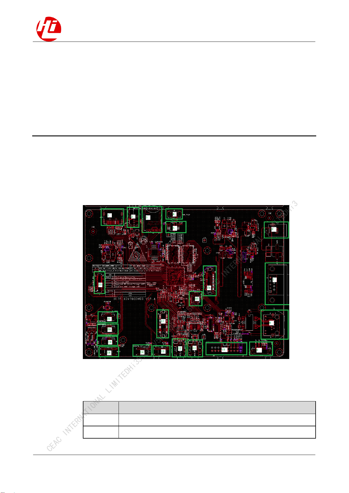
Figure 2-1 shows the interfaces on the Hi3516D V300 demo board.
Figure 2-1 Interfaces on the Hi3516D V300 demo board
Table 2-1 describes the corresponding peripheral interfaces, keys, and switches in Figure 2-1.
Table 2-1 Peripheral interfaces on the Hi3516D V300 demo board
No.
Description
1
HDMI
2
USB 2.0 port
CEAC INTERNATIONAL LIMITEDHi3516C V500R001C02SPC001CEAC INTERNATIONAL LIMITEDHi3

Hi3516D V300 Demo Board
User Guide
2 Hardware
Issue 00B01 (2018-09-04)
HiSilicon Proprietary and Confidential
Copyright © HiSilicon Technologies Co., Ltd.
3
No.
Description
3
SD card holder
4
Testing interface for the core power and DDRIO power
5
Dual in-line package (DIP) SW3
6
Board power interface
7
UART0 port
8
RJ45 megabit Ethernet port
9
I2S interface
10
JTAG interface
11
ADUIO_OUT
12
AUDIO_IN
13
KEY1
14
UPDATE_MODE key
15
Liquid crystal display (LCD) connector
16
SW1
17
SDIO1 Wi-Fi connector
18
KEY2
19
UART1 port
20
DC-IRIS interface
21
P-IRIS interface
22
60-pin sensor interface
2.2 GPIO Distribution
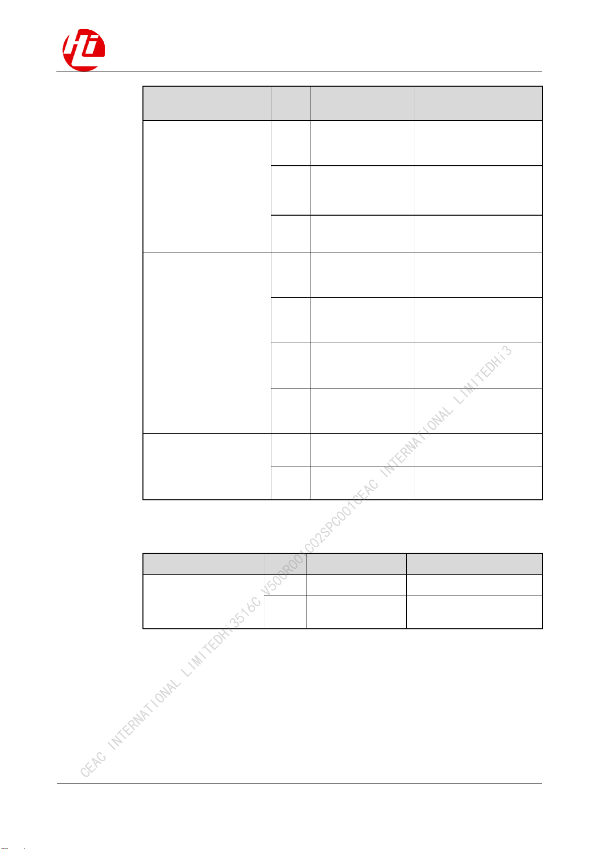
Table 2-2 describes the GPIO distribution of the Hi3516D V300 demo board.
Table 2-2 GPIO distribution of the Hi3516D V300 demo board
Pin
GPIO Pin
DMEB Board
I2C7_SCL/GPIO10_6
GPIO10_6
Test point
I2C7_SDA/GPIO10_7
GPIO10_7
Test point
PWM1/GPIO6_7
GPIO6_7
DC_IRIS_PWM4/PWM_OUT0_LCD.
PWM_OUT0_LCD is used by default.
CEAC INTERNATIONAL LIMITEDHi3516C V500R001C02SPC001CEAC INTERNATIONAL LIMITEDHi3

Hi3516D V300 Demo Board
User Guide
2 Hardware
Issue 00B01 (2018-09-04)
HiSilicon Proprietary and Confidential
Copyright © HiSilicon Technologies Co., Ltd.
4
Pin
GPIO Pin
DMEB Board
UART1_CTSN/GPIO
5_1/UART4_TXD
GPIO5_1
WIFI_LED control. The indicator is on when
the output is high level and off when the
output is low level.
UART1_RTSN/GPIO
5_0/UART4_RXD
GPIO5_0
UPDATE_LED control. The indicator is on
when the output is high level and off when
the output is low level.
LSADC_CH1/GPIO10
_4
GPIO10_4
Connects to the SGM8903 mute pin.
GPIO0_3/IR_IN/LCD
_DATA18
GPIO0_3
TP_RST and P_IRIS_CONTROL1 are
multiplexed. TP_RST is used by default.
GPIO0_4/LCD_DAT
A21
GPIO0_4
TP_INT and P_IRIS_CONTROL2 are
multiplexed. TP_INT is used by default.
GPIO0_5/LCD_DAT
A22
GPIO0_5
LCD_RST and P_IRIS_CONTROL3 are
multiplexed. LCD_RST is used by default.
GPIO0_6/LCD_CLK/
VOU_CLK
GPIO0_6
DIS_FLOW_CTRL and
P_IRIS_CONTROL4 are multiplexed.
DIS_FLOW_CTRL is used by default.
CEAC INTERNATIONAL LIMITEDHi3516C V500R001C02SPC001CEAC INTERNATIONAL LIMITEDHi3

Hi3516D V300 Demo Board
User Guide
3 Operation Guide
Issue 00B01 (2018-09-04)
HiSilicon Proprietary and Confidential
Copyright © HiSilicon Technologies Co., Ltd.
5
3 Operation Guide
3.1 Precautions
The Hi3516D V300 demo board applies to the laboratory or engineering development
environment. Take the following precautions before performing operations:
CAUTION
Never perform the hot-swap operation on the board in any case.
Take antistatic measures before unpacking or installing the board to prevent the board
hardware from being damaged by the electrostatic discharge (ESD).
Hold the board on the edge and do not touch the exposed metal on the board. Otherwise,
the board components may be damaged by the ESD.
Place the Hi3516D V300 demo board on a dry workstation and keep it away from heat
sources, electromagnetic interference sources, radiant sources, and electromagnetic
susceptibility equipment (such as the medical equipment).
Familiarize yourself with the layout of the Hi3516D V300 demo board. See Figure 2-1.
Ensure that you can identify the components such as the switches, connectors, and
indicators and know their positions.
3.2 Board Settings
The operating mode of the Hi3516D V300 is selected by using the keys and selecting the
resistors to be welded on the Hi3516D V300 demo board. See Table 3-1.
Table 3-1 Board settings in various boot modes
Boot Mode
Value
Resistor
Connection
Remarks
BOOT_SEL[1:0]
00
SW1.4 and SW1.3
are set to 0.
Boot from the SPI flash.
CEAC INTERNATIONAL LIMITEDHi3516C V500R001C02SPC001CEAC INTERNATIONAL LIMITEDHi3
Hi3516D V300 Demo Board
User Guide
3 Operation Guide
Issue 00B01 (2018-09-04)
HiSilicon Proprietary and Confidential
Copyright © HiSilicon Technologies Co., Ltd.
6
Boot Mode
Value
Resistor
Connection
Remarks
01
SW1.4 is set to 0,
while SW1.3 is set to
1.
Boot from the eMMC.
10
SW1.4 is set to 1,
while SW1.3 is set to
0.
Fastboot
Update SPI flash
(default)
11
SW1.4 and SW1.3
are set to 1.
Fastboot
Update eMMC (default)
[SFC_DEVICE_MODE:
SFC_BOOT_MODE]
00
SW1.1 is set to 0,
R188 is removed,
and R367 is soldered.
SPI NOR flash. The default
addressing mode is 3-byte
mode.
01
SW1.1 is set to 0,
R367 is removed,
and R188 is soldered.
SPI NOR flash. The default
addressing mode is 4-byte
mode.
10
SW1.1 is set to 1,
R188 is removed,
and R367 is soldered.
SPI NAND flash. The
default addressing mode is
1-wire boot mode.
11
SW1.1 is set to 1,
R367 is removed,
and R188 is soldered.
SPI NAND flash. The
default addressing mode is
4-wire boot mode.
UPDATE_MODE
0
S3 key is pressed
down.
Enable update from SDIO0
or USB.
1
S3 key is not pressed
down.
Disable UPDATE_MODE
(default).
Table 3-2 JTAG settings
Boot Mode
Value
Instructions
Remarks
JTAG/SPI1/I2S
0
SW3.1 is set to 0.
JTAG
1
SW3.1 is set to 1.
SPI1/I2S (SPI1 and I2S are
soldered by using resistors.)
3.3 DIP Switch Usage
As shown in Figure 3-1, the pin1 side of the DIP switch is 1while the other side is 0.
CEAC INTERNATIONAL LIMITEDHi3516C V500R001C02SPC001CEAC INTERNATIONAL LIMITEDHi3

Hi3516D V300 Demo Board
User Guide
3 Operation Guide
Issue 00B01 (2018-09-04)
HiSilicon Proprietary and Confidential
Copyright © HiSilicon Technologies Co., Ltd.
7
Figure 3-1 Diagram of DIP switch usage
CEAC INTERNATIONAL LIMITEDHi3516C V500R001C02SPC001CEAC INTERNATIONAL LIMITEDHi3
Table of contents
Other HiSilicon Motherboard manuals


