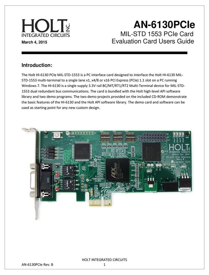
HOLT ADK-2130mPCIe User manual

QSG-2130mPCIe_New 1/20
ADK-2130mPCIe
Quick Start Guide
Dec, 20 2019

REVISION HISTORY
Revision
Date
Description of Change
QSG-2130mPCIe
Rev. New
1/20/19
Initial Release

Holt Integrated Circuits
3
Introduction
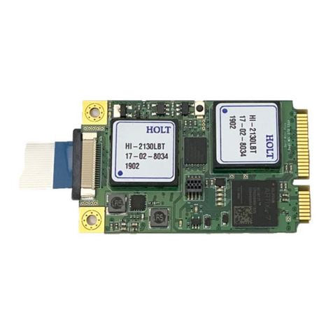
The Holt Mini PCIe Mini card reference design features one or two Holt HI-2130 MIL-STD 1553 multi-
channel dual redundant terminals with integrated transformers on a single size F2 Mini PCIe card. The
card is designed to operate in a PC with a Linux OS. The Demo software uses the Holt API Library functions,
providing an abstraction layer that greatly simplifies host programming. A console menu is presented in a
terminal window where commands are executed. This Quick Start Guide provides instructions how to
boot from the Holt Flash Drive and run the demonstration software.
Figure 1 –Mini PCIe card EV-2130mPCIe-2F
Figure 2 –Mini PCIe breakout board mPCIe_breakout-2F

Holt Integrated Circuits
4
Kit Contents
Quick Start Guide (QSG-2130mPCIe).
Mini PCIe card, Single HI-2130: EV-2130mPCIe-1F or Dual HI-2130: EV-2130mPCIe-2F.
USB 3.0 128G flash drive with Bootable Ubuntu 16.04.6 LTS, 18.04 LTS.
Holt Eclipse and Vivado projects.
Mini PCIe Technical Manual (AN-2130mPCIe.
Optional Break Out board:
omPCIe_Breakout-1F (single channel) or mMPCIe_Breakout-2F (dual channel).
Quick Start Demo Requirements
PC requirements:
oMini PCIe Slot.
oUSB 3.0 port. USB 2.0 may not be bootable or will operate very slow - not
recommended.
o4G RAM minimum. 8-16G is recommended for Eclipse and Vivado use –not required
for the QSG demos presented here.
Demo configurations
The cables on the Break Out board should be connected to a MIL-STD 1553 bus coupler. See AN-551 for
recommended bus connections.
The Holt Break Out board is connected to the Mini PCIe card using a small ribbon cable. The cable
connector strain reliefs are delicate so care must be exercised to avoid damage. Since the HI-2130 shares
the same 1553 bus pins (BUSA, nBUSA) with all four internal terminals (BC, RT, RT2 and SMT) in each
device, the RT responds to commands transmitted by the BC in the same device.

Holt Integrated Circuits
5
Tripple BUCK
Power supply
LTC3545 (1 spare)
3.3VMOSFET
switch
100MHz
MEMS
OSC
Quad SPI
FLASH
JTAG
8 pin
to
FPGA
3.3aux
VCCINT 1V
MGTAVCC1V
VCC1.8V
(JTAG)
VCCO
3V3
52 pin
PCIe
conn.
Xilinx ARTIX-7
XC7A127-2CPG238I
10 x 10
HI-2130
(36) 16 bit address/data EBI
(6) Int,int,RTxMC8
nCS, nWE, nRD, TEST,MCLK, nMR,
TXINHA/B
PCIe
x1 lane
2x1.6
4x4 14.99 sq.
14.99 sq.
3.3aux
Optional
TBD 6x LED’s:
done, init_b,
rst, urst,
pcie_link,
heartbeat.
Bank 34
HI-2130-1
HI-2130-2
PCIe TX,RX, REFCLK
Bank 14
Bank 14Bank 16
JTAG,Misc Bank 0
ACTIVE TP
14.99mm sq.
TXHIBx,BCENA,BCTRIG AND 1553 BUS
1V
reg
MGTAVTT1V2
1V
reg
1V5
GOOD
1V5
J4
Figure 3 –Mini PCIe board block diagram
Table 1 –LEDs
PWR D1, Green
VCCO3V3 switched power.
Done D2, Green
FPGA initialized from SPI Flash
Complete D3, Green
FPGA initialize complete.
LED D6, Green
FPGA rst signal
LED D7, Green
FPGA urst signal
LED D8, Green
FPGA PCIe Link Up –must be on for
the card to work.
LED D9, Green
FPGA Heart Beat

Holt Integrated Circuits
6
Getting Started
The Holt USB 3.0 flash drive (FD) contains a bootable version of Ubuntu Linux. The Home folder contains
the project folders and script files to run the Demos. Booting from the Holt FD allows running the Demo
in the fewest steps possible since the Demo and kernel module was prebuilt for the Ubuntu and kernel
version installed on the FD. The user cannot just copy the files from the FD to the user’s PC and run the
demo program following these instructions, unless the OS and kernel versions are the same.
This Quick Start Guide assumes the user boots from the Holt FD. If the user’s PC does not have a
bootable USB 3.0 port the following instructions cannot be used. Refer to the Holt Technical Manual for
instructions how to transfer the projects to a new computer and install Eclipse and rebuild the kernel
module and Demo program.
Quick Start Demo Instructions –using the Holt USB 3.0 FD booted on a PC
These instructions assume the user has Linux experience using terminal commands.
1. Turn off the PC and install the Holt Mini PCIe card.
2. Carefully insert the small ribbon cable to the Mini Card J4 connector and the other end to the
Break Out board. The cable is fine pitched and the connector plastic fasteners are delicate so care
must be exercised to avoid damaging the connector.
3. Insert the Holt FD into a USB 3.0 port.
4. Before turning on the PC the user should be familiar how to boot from the external USB FD.
Typically, the F11 or F12 key is quickly pressed after a BIOS screen is briefly displayed showing
some boot options. The computer shows a boot up menu showing possible drives that are
bootable.
5. Use the up or down arrow keys to select the Holt USB FD to boot from. Identify the Holt USB FD
by the manufacturer name on the FD such as “SanDisk or Memorex”. Select the Holt USB FD and
press enter. The computer should begin the boot sequence from the Holt USB FD. An Ubuntu
screen is displayed with an Ubuntu selection at the top, the user can wait for it to boot or press
the enter key to start the boot-up immediately.
6. When the desktop appears enter “holtpcie” for the password. The same password is used for
some terminal commands requiring sudo privileges.
7. Use the Ubuntu “Files” application shown on the launch menu on the left side of the desktop
screen that looks like a file cabinet to navigate to folders and view files in the Holt folder.

Holt Integrated Circuits
7
8. Double click the ‘Holt’ folder to preview the Holt folder containing two project folders, bash
scripts and documents.
The program initializes the four RT’s with the following RT addresses (these can be changed later
using command ‘9’). In some demos and in the software RT1 may also be referred to as RT. RT2
will always be referred to RT2.
Table 2 –Device RT Addresses
DEVICE/IC
RT
RT ADDRESS
ADK Board
Dev 0 / U7
RT (RT1)
3
ADK-2130mPCIe-1F
Dev 0 / U7
RT2
1
ADK-2130mPCIe-1F
Dev 1 / U8
RT (RT1)
3
ADK-2130mPCIe-1F
ADK-2130mPCIe-2F
Dev 1 / U8
RT2
1
ADK-2130mPCIe-1F
ADK-2130mPCIe-2F
9. Open a terminal window in the Holt folder and execute the ‘run’ script.

Holt Integrated Circuits
8
10. Linux will ask for the password, enter “holtpcie” and press return. The ‘run’ scripts checks the OS
to see if the Xilinx Device 7011 PCIe device is found then executes two bash scripts to unload and
reload the kernel module and lastly runs the Demo executable.
The ‘unload’ script will be explained in the Technical Manual and is not used in this QSG. LED8
‘LINK’ is an indicator that the PCIe OS link was successful. If this LED is not “on”, the board will not
work. See trouble shooting section at the end of this document. If the console shows the message
below “…Xilinx Corporation Device 7011” then it was OK.
holt@holt-desktop:~/holt$ sh run
06:00.0 Memory controller: Xilinx Corporation Device 7011
[sudo] password for holt:
Holt Linux driver unloaded
Holt Linux driver loaded
1553LibrarySrc_linkedfolder Demo _HI-613x_LINUX_DEMO makefile
objects.mk sources.mk
Setting nMR chan 0 LOW Setting nMR chan 0 HIGH READY asserted
Setting nMR chan 1 LOW Setting nMR chan 1 HIGH READY asserted
Number of Devices found: 2
Initial default RT addresses:
DEV0:RT1=3 DEV0:RT2=1 DEV1:RT1=3 DEV1:RT1
Optionally use console command '9' to change these RT addresses
BEFORE RUNNING RT
*************************************************
Holt Integrated Circuits
Mini PCIe Dual HI-2130 API Demo
Demo Rev: 1.0 Compiled: Dec 11 2019 08:41:16
API Lib Rev: 03-5-0
*************************************************
BC On SMT On RT1 On RT2 On
Press 'a' or 'A' to run Dev0 or Dev1 BC Async demo.
Press 'b' or 'B' to run Dev0 or Dev1 RT demo.
Press 'c' or 'C' to run Dev0 or Dev1 RT2 demo.
Press 'k' or 'K' to Enable Dev0 or Dev1 RTMT.
Press 'l' or 'L' to send high priority BC message.
Press 'h' or 'H' to send low priority BC message.
Press 'n' or 'N' to run Dev0 or Dev1 BC Major Minor Frame demo.
Press 'x' or 'X' to stop Dev0 or Dev1 BC transmissions.
Press 'S' to run SMT demo.
Press 't' to display RT Traffic Toggle.
------------ Utilities -------------
Press 'r' or 'R' to Display Dev0 or Dev1 HI-2130 Registers.
Press 'w' for Memory Watch window
Press 'f' Reads J4 connector and FPGA control signals
Press '1' for Register Write
Press '2' for Memory Write

Holt Integrated Circuits
9
Press '3' RT Mode Code data word reads
Press '4' Master Reset and reinitializes terminals
Press '5' Toggle Dev0 BCENA on/off
Press '6' Toggle Dev1 BCENA on/off
Press '9' Set RT addresses
Press '0' Toggle between User and Demo(default) modes
Press 'M' for menu, or press any valid menu key. >>
The menu commands are very similar to other Holt ADK’s such as the ADK-6138, ADK-6130-2 or
ADK-6131. Lower case characters ‘a’, ‘n, ‘b’, ‘c’ and ‘r’ executes commands on the (Dev0) and ‘A’,
‘N’, ‘B’, ‘C’ and ‘R’ executes commands on Dev1. With a -1F card (only one HI-2130) the upper
case commands will not be presented.
Command ‘r’ and ‘R’ is used to display system registers names and values on the screen.
Command ‘w’ displays a memory dump of device memory showing up to 256 words. This is useful
for viewing other areas of memory such as the illegalization tables, control blocks and data
buffers.
Demo exercises using Device 0
1. BC transmits 15 messages and RT1 captures and displays the traffic data.
Commands ‘n’ or ‘N’ initializes the BC to transmit 15 messages. To display RT data traffic some
additional commands must first be executed. Five sets of three repeating messages are transmitted
by the BC. SA30 is configured for data loop-back. So the data transmitted to the RT from the first
Receive command is loaded into the same buffer location the RT will reference when transmitting
data back to the BC. Just these three commands verify that both A and B buses are properly
communicating with the BC. The data word values will match the data from the first Receive
command.
BC > RT Receive Cmd, SA30, 32 words, BusA: 03-R-30-00
RT > BC Transmit Cmd, SA30, 32 words, BusB 03-T-30-00
RT > BC Transmit Cmd, SA30, 32 words, BusA 03-T-30-00
Enter ‘b’ to enable Dev0 RT1
Enter ‘k’ to enable Dev0 RT1 with SMT
Enter ‘t’ to enable RT traffic data displayed on the screen.
Enter ‘n’ to transmit 15 messages and stops.
The display should look similar to this below.
Press 'M' for menu, or press any valid menu key.
>> b
>k
RTMT Demo
>t
Holt Integrated Circuits
10
Traffic Enabled
>n
>
Dev0 MSG #0000. TIME = 00040628us BUS A TYPE0: BC to RT
CMD1 1BC0 --> 03-R-30-00
DATA 0101 0202 0303 0404 0505 0606 0707 0808
0909 1010 1111 1212 1313 1414 1515 1616
1717 1818 1919 2020 2121 2222 2323 2424
2525 2626 2727 2828 2929 3030 3131 3232
STA1 1800
Dev0 MSG #0001. TIME = 00041324us BUS B TYPE1: RT to BC
CMD1 1FC0 --> 03-T-30-00
STA1 1800
DATA 0101 0202 0303 0404 0505 0606 0707 0808
0909 1010 1111 1212 1313 1414 1515 1616
1717 1818 1919 2020 2121 2222 2323 2424
2525 2626 2727 2828 2929 3030 3131 3232
Dev0 MSG #0002. TIME = 00042020us BUS A TYPE1: RT to BC
CMD1 1FC0 --> 03-T-30-00
STA1 1800
DATA 0101 0202 0303 0404 0505 0606 0707 0808
0909 1010 1111 1212 1313 1414 1515 1616
1717 1818 1919 2020 2121 2222 2323 2424
2525 2626 2727 2828 2929 3030 3131 3232
Dev0 MSG #0003. TIME = 00042720us BUS A TYPE0: BC to RT
CMD1 1BC0 --> 03-R-30-00
DATA 0101 0202 0303 0404 0505 0606 0707 0808
0909 1010 1111 1212 1313 1414 1515 1616
1717 1818 1919 2020 2121 2222 2323 2424
2525 2626 2727 2828 2929 3030 3131 3232
STA1 1800
Dev0 MSG #0004. TIME = 00043416us BUS B TYPE1: RT to BC
CMD1 1FC0 --> 03-T-30-00
STA1 1800
DATA 0101 0202 0303 0404 0505 0606 0707 0808
0909 1010 1111 1212 1313 1414 1515 1616
1717 1818 1919 2020 2121 2222 2323 2424
2525 2626 2727 2828 2929 3030 3131 3232
2. BC Transmits Major frames and Minor frames
Command ‘a’ demonstrates the BC transmitting a continuous stream of messages in a
Major/Minor frame format. To stop transmissions press ‘x’ followed by return. Only the first
seven messages are shown here. Since the RT and SMT and traffic commands were already
enabled from the last demo, press ‘a’ to execute this demo. Notice the RT to RT messages have
a ‘no response’ error –this is because RT2 has not been enabled.

Holt Integrated Circuits
11
a
>
Dev0 MSG #0015. TIME = 00004238us BUS A TYPE0: BC to RT
CMD1 1822 --> 03-R-01-02
DATA 0005 0002
STA1 1800
Dev0 MSG #0016. TIME = 00004286us BUS A TYPE2: RT to RT
CMD1 182A --> 03-R-01-10
CMD2 0C2A --> 01-T-01-10
ERROR: NORES
Dev0 MSG #0017. TIME = 00004352us BUS A TYPE2: RT to RT
CMD1 182A --> 03-R-01-10
CMD2 0C2A --> 01-T-01-10
ERROR: NORES
Dev0 MSG #0018. TIME = 00004416us BUS B TYPE2: RT to RT
CMD1 182A --> 03-R-01-10
CMD2 0C2A --> 01-T-01-10
ERROR: NORES
Dev0 MSG #0019. TIME = 00104176us BUS A TYPE0: BC to RT
CMD1 1822 --> 03-R-01-02
DATA 0005 0002
STA1 1800
Dev0 MSG #0020. TIME = 00104224us BUS A TYPE2: RT to RT
CMD1 182A --> 03-R-01-10
CMD2 0C2A --> 01-T-01-10
ERROR: NORES
Dev0 MSG #0021. TIME = 00104290us BUS A TYPE2: RT to RT
CMD1 182A --> 03-R-01-10
CMD2 0C2A --> 01-T-01-10
ERROR: NORES

Holt Integrated Circuits
12
3. Enable RT2.
If the previous BC messages are still transmitting, press the ‘x’ key followed by return to stop the
BC. Press the ‘c’ command to enable RT2 which is set to RT address 1.
4. Press ‘a’ again and this time the RT to RT messages will both respond properly without any ‘no
response’errors. Press ‘x’ and return to stop the BC to view messages. Only some messages are
shown below.
>c
>a
>
Dev0 MSG #0043. TIME = 00127134us BUS A TYPE0: BC to RT
CMD1 1822 --> 03-R-01-02
DATA 0005 0002
STA1 1800
Dev0 MSG #0044. TIME = 00127436us BUS A TYPE2: RT to RT
CMD1 182A --> 03-R-01-10
CMD2 0C2A --> 01-T-01-10
STA1 0800
DATA BBBB 0202 1414 0404 0505 0606 0707 0808
0909 1010
STA2 1800
Dev0 MSG #0045. TIME = 00096012us BUS A TYPE0: BC to RT
CMD1 1822 --> 03-R-01-02
DATA 0005 0002
STA1 1800
Dev0 MSG #0046. TIME = 00096316us BUS A TYPE2: RT to RT
CMD1 182A --> 03-R-01-10
CMD2 0C2A --> 01-T-01-10
STA1 0800
DATA BBBB 0202 1414 0404 0505 0606 0707 0808
0909 1010
STA2 1800
Dev0 MSG #0047. TIME = 00064942us BUS A TYPE0: BC to RT
CMD1 1822 --> 03-R-01-02
DATA 0005 0002
STA1 1800

Holt Integrated Circuits
13
Demo exercises using Device 1: ADK-2130mPCIe-2F
To demonstrate the second HI-2130 (Dev1), a Holt IC card with two HI-2130’s is required, PN ADK-
2130mPCIe-2F. Execute the same commands but with Upper case letters.
Press ‘B’, ‘K’ and ‘N’ all in upper case to exercise the second HI-2130 (Dev1) BC and RT1. Notice ‘Dev1” is
shown instead of ‘Dev0’ as in the previous exercises. The N command transmits the same 15 messages,
(3 are shown below,) but this time the BC in the second HI-2130 (Dev1) is used.

Holt Integrated Circuits
14
Demonstrating the Holt Mini PCIe RT with an external BC.
Any one of the four RT’s can be used with an external BC tester. Choose the desired channel and set the
RT address to match the BC message using command ‘9’. Connect the external BC to a bus coupler and
connect a stub from the bus coupler to the BNC connector on the optional Holt breakout board. See AN-
551 for proper bus connections.
To change the RT terminal address, press ‘9’ BEFORE enabling the RT. If a RT was enabled by a ‘b’,B’ ‘c’
or ’C’ command use command ‘4’ to reset the card first. The program first prompts for the channel
number 0-4 followed by the RT address value.
Table 3 –Device RT Addresses and Channels
DEVICE/IC
RT
DEFAULT RT
ADDRESSES
Command 9 channel
Dev 0 / U7
RT (RT1)
3
0
Dev 0 / U7
RT2
1
1
Dev 1 / U8
RT (RT1)
3
2
Dev 1 / U8
RT2
1
3
Enable the RT with a corresponding ‘c’, ‘C’, ‘b’ or ‘B’ command depending on which RT and channel is
used.
Enable ‘k’ or ‘K’ and ‘t’. The RT is ready for BC command reception. Make sure the external BC message
tester is set for the corresponding RT address or the message will be ignored. Traffic data display using
the ‘t’ command is optional but is recommended when first learning the card. BC message transaction
occurs whether or not the ‘t’ command is used since ‘t’ just enables the ability to display the data on the
console.

Holt Integrated Circuits
15
Demonstrating the Holt Mini PCIe BC with an external RT.
The BC demos transmit messages to RT addresses 3 and 1. To change these RT addresses the program
must be modified and recompiled. See the Technical Manual for instructions on how to do this.
Connect the external RT to one of the tri-axial jacks on the break out board. A bus coupler should be used
to connect the external RT to the card BC. See AN-551 for proper bus connections.
A possible bus conflict will occur if any of the on-card RTs has the same RT address. In this case change
the RT address using command ‘9’ to a different value or use command ‘4’ to reset the card and reinitialize
the terminals. This time don’t enable any of the cards RT’s.
Use command ‘n’ or ’N’ to command the BC to transmit messages. The external RT should receive the
message if the RT address matches the RT address in the BC command word, which for this card is either
3 or 1. To modify the BC commands for a different RT address see the Technical Manual.

Holt Integrated Circuits
16
Table 4 –Connector J-4 pin-out
20 Pin
NAME
DESCRIPTION
1
CHANNEL 0 APOS
MIL-STD-1553 CH0 A+ (BUSA)
2
CHANNEL 0 ANEG
MIL-STD-1553 CH0 A- (nBUSA)
3
Chassis GND
Mounting screw –no other connection.
4
CHANNEL 0 BPOS
MIL-STD-1553 CH0 B+ (BUSB)
5
CHANNEL 0 BNEG
MIL-STD-1553 CH0 B- (nBUSB)
6
Chassis GND
Mounting screw –no other connection.
7
CHANNEL1 APOS
MIL-STD-1553 CH1 A+
8
CHANNEL 1 ANEG
MIL-STD-1553 CH1 A-
9
Chassis GND
Mounting screw –no other connection.
10
CHANNEL 1 BPOS
MIL-STD-1553 CH1 B+
11
CHANNEL 1 BNEG
MIL-STD-1553 CH1 B-
12
Chassis GND
Mounting screw –no other connection.
13
CH0INHBIT0
Channel 0 Transmit Inhibit. 10K pull-up.
Connects to an inverter which Inverted
direct connect to 2130 inhibit pins.
14
CH0 BCENAB
Channel 0 BC Enable. 10K pull-up.
15
CH0 BCTRIG
Channel 0 BC Trigger. 10K pull-up.
16
SPARE INPUT
Unused.
17
CH1INHBIT1
Channel 0 Transmit Inhibit. 10K pull-up.
Inverted direct connect to 2130 inhibit
pins.
18
CH1 BCENAB
Channel 1 BC Enable. 10K pull-up.
19
CH1 BCTRIG
Channel 1 BC Trigger. 10K pull-up.
20
Logic GND

Holt Integrated Circuits
17
Trouble shooting
1. Booting from the Holt USB Flash Drive. There are typically a few seconds from powering a PC to
when a short DOS like message appears to allow pressing F11 or F12 to enter a boot menu.
Some PC’s might be configured to bypass in the bios. Check with your company IT person to see
if they can help resolve this issue since they may already be familiar with the PC bios settings.
Holt is not in a good position to assist with these types of PC problems.
2. If the PCIe Link fails (LED8 OFF), power off the PC and try uninstalling the card and reinstalling
the card again to ensure a good fit. If the PC does not supply 1.5V on the PCIe Mini slot this will
also cause a link failure. Check with the PC motherboard manual to see if there’s a way to
enable the 1.5V. The card requires 1.5V and there is no way to make it work without 1.5V.
The ‘run’ script includes this terminal command which can be executed separately in a terminal
window to see if Linux detected the PCIe link.
holt@holt-desktop:~/holt$ lspci | grep Xilinx
If this was displayed then the link was OK.
“Memory controller: Xilinx Corporation Device 7011”
3. In some rare cases if the Demo fails to run try rebooting the PC and try again.
4. If 1553 bus traffic does not appear on the cable connectors try unplugging the ribbon cable from
the card and break out board and reinsert it again while trying to make sure it as straight as
possible.
Summary
This quick start guide provided simple steps on how to use the Holt Flash Drive to demonstrate Holt’s Mini
PCIe card. When booting from the Holt FD a minimal amount of work is required to run the demo since
all the software is preinstalled. This is meant as an introduction to the use of the card and demo software.
To learn more about the design including using the development tools refer to the Technical Manual.
To install the Holt demo project and import the projects into Eclipse to build and run the demo project
on the user’s PC, see the technical guide.
Other manuals for ADK-2130mPCIe
3
Table of contents
Other HOLT PCI Card manuals