HOLT ADK-2130mPCIe User manual

AN-2130mPCIe_New 01/20
ADK-2130mPCIe
Technical Manual
Jan. 16, 2020

This page intentionally blank

Holt Integrated Circuits
3
REVISION HISTORY
Revision
Date
Description of Change
AN-2130mPCIe
Rev. New
1/16/20
Initial Release

Holt Integrated Circuits
4
Introduction
The Holt full size F2 Mini PCIe card reference design features one or two Holt HI-2130 MIL-STD 1553
multi-channel terminals with integrated transformers on a single Mini PCIe card. The card is designed to
operate in a PC or single board computer with a Linux OS (note: Windows support will be available in the
near future). The Demo software uses the Holt API Library functions, providing an abstraction layer that
greatly simplifies host programming. This Technical Manual covers the hardware, software and
instructions for how to transfer the Holt Flash Drive (FD) files to the user’s PC. See the Quick Start Guide
(QSG) for an introduction to the card, Application Development Kit (ADK) contents and how to run the
demonstration software using the Holt bootable Flash Drive. Use the instructions in this guide to install
the Holt software and Eclipse IDE tool used for software development on to a user’s PC. Use the
instructions in the QSG when booting from the Holt USB FD. See technical guide AN-PCIeFPGA for the
FPGA design.
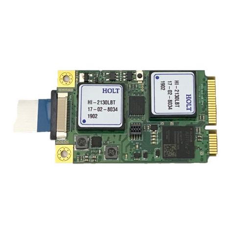
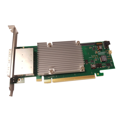
Figure 1 –Mini PCIe card EV-2130mPCIe-2F
Features
Mini PCIe F2 full size, PCIe gen2 single lane
Single Channel ADK-2130mPCIe-1F or Dual channel ADK-2130mPCIe-2F
Mini Card Electromechanical Specification Rev. 1.2
Independent two dual-redundant MIL-STD 1553 channels using proven HI-2130’s
Each Channel with BC, Dual RT and MT
Transformer coupled MIL-STD 1553 interface
Holt API Library support
Linux OS
Operating temperature -40° to +85°
Customizable FPGA
Demo software for BC, RT, RT2 and MT

Holt Integrated Circuits
5
PC requirements
Linux OS: Ubuntu: 16.04.6 LTS or 18.04 LTS (Holt FD installed).
System RAM: 8G is recommended for Eclipse, 16G for Vivado.
Hard Drive Capacity: 10G minimum for the Eclipse project.
Mini PCIe Slot Standard Full size F2
USB 2.0 or 3.0 Port: For transferring Holt Flash Drive files.
Mini PCIe board block diagram
Tripple BUCK
Power supply
LTC3545 (1 spare)
3.3VMOSFET
switch
100MHz
MEMS
OSC
Quad SPI
FLASH
JTAG
8 pin
to
FPGA
3.3aux
VCCINT 1V
MGTAVCC1V
VCC1.8V
(JTAG)
VCCO
3V3
52 pin
PCIe
conn.
Xilinx ARTIX-7
XC7A127-2CPG238I
10 x 10
HI-2130
(36) 16 bit address/data EBI
(6) Int,int,RTxMC8
nCS, nWE, nRD, TEST,MCLK, nMR,
TXINHA/B
PCIe
x1 lane
2x1.6
4x4 14.99 sq.
14.99 sq.
3.3aux
Optional
TBD 6x LED’s:
done, init_b,
rst, urst,
pcie_link,
heartbeat.
Bank 34
HI-2130-1
HI-2130-2
PCIe TX,RX, REFCLK
Bank 14
Bank 14Bank 16
JTAG,Misc Bank 0
ACTIVE TP
14.99mm sq.
TXHIBx,BCENA,BCTRIG AND 1553 BUS
1V
reg
MGTAVTT1V2
1V
reg
1V5
GOOD
1V5
J4

Holt Integrated Circuits
6
Break Out Board
The Break Out board connects to the PCIe card through a ribbon cable and is used to break out both
BusA and BusB connections from both channels (Dev0 and Dev1). The Transmit Inhibits inputs are pulled
high which present a low to the HI-2130 devices which enables 1553 bus transmissions by default. Table
8 is a list of the signals and descriptions on the inter-connect ribbon J4 connector. For board component
locations, connectors, IC’s and test points, see Figure 3 –Board References at the end of the document.
Two break-out boards are available.
Single channel: mPCIe_breakout-1F
Dual channel: mPCIe_breakout-2F
Figure 2 –mPCIe_breakout-2F break-out board

Holt Integrated Circuits
7
First Things First
In order to successfully execute the Holt demo program the PC must be able to detect the card’s PCIe
interface at power up.
1. Reviewing the Holt QSG-2130mPCIe.pdf prior to reading this document is highly recommended.
2. Linux experience and the terminal window with the command line are highly recommended.
3. Power down the PC and install the Holt Mini PCIe card. Connecting the break-out board is not
critical for this step so is optional.
4. The Ubuntu OS on the Holt FD cannot be used to install Ubuntu on a user’s PC. If the user has an
older version of Ubuntu than 18.04 LTS it may be possible to upgrade it.
We recommend downloading Ubuntu 18.04 LTS from the Ubuntu website and using the
provided installation instructions. Holt has not tried any other Linux version as of this date.
Windows support is planned in the future.
https://ubuntu.com/#download
5. Power up the PC. Shortly after powering up the computer the green PCIe Link LED 8 should be
on and the Heart Beat LED 9 should flash on and off.
6. When LED 8 illuminates, the computer boot up sequence has detected the PCIe link on the card.
Another way to verify this is to open a terminal window and execute the following command.
holt@holt-desktop:~/holt$ lspci | grep Xilinx
“Memory controller: Xilinx Corporation Device 7011”
If this is displayed the PC successfully detected the PCIe link.
If the ‘Xilinx Corporation Device 7011” was not displayed try turning off the PC and reinstalling
the card making sure the card is fully plugged in. If the LED’s never light up it might be due to
missing 1.5V on the Mini PCIe slot. Refer to the PC motherboard manual to see if 1.5V needs to
be enabled by a configuration or jumper setting. Another PC may need to be used.
Holt Integrated Circuits
8
PC preparation for installing Eclipse and the Holt software
The Eclipse C/C++ IDE tool is free from www.eclipse.org and is used for this project. If Eclipse is already
installed this step can be bypassed.
1. Java JRE must be installed. Open a terminal window and type “sudo apt install default-jre”and
press return. Confirm the installation and press (Y). After Java is installed enter “java –version”
to see a message with a version to confirm the installation.
2. Go to the eclipse download page and download software. If using the eclipse installer select the
C/C++ package. After the installation is complete optionally launch eclipse to see it working then
exit the program. It’s possible to create a program short-cut from a terminal window where
eclipse is installed then drag the link to the desktop. Navigate to where Eclipse is installed and
right click on the eclipse program icon and select “Make Link” to create a link. Drag the link to the
desktop.
The Holt demo software is comprised of three project sub-folders residing in a single Eclipse workspace
folder.
3On the Ubuntu OS home folder create a Holt folder.
Copy all the folders, script files and other miscellaneous documents from the Flash Drive to the
newly created Holt folder on the PC. The folder and files should appear similar to this.
3. Launch Eclipse and use the Browse button to select the project folder shown below and click the
OK button.

Holt Integrated Circuits
9
4. When Eclipse opens the project the first time the projects must be imported. If the Eclipse Project
Explorer (PE) window isn’t shown type in “Project Explorer”into the Quick Access window located
on the top right corner of the screen and select it from the list of items shown. The three project
folder should be shown in the PE.
5. Project descriptions for the three project are contained in sub-folders:

Holt Integrated Circuits
10
Demo –The Demo software resets both devices and initializes both devices using the Holt API
library functions. There are two build configurations: Debug and Debug_precompiled_library. The
Debug_precompiled_library requires a binary library file produced by the H1553Libary project.
See below. Rebuilding the ‘Debug’ configuration compiles all the demo files including the Holt API
library files and outputs the Demo executable.
H1553Libary –This project builds the API library output file libH1553Library.a that is linked with
the Debug_precompiled_libary target demo project above.
pcie_kernel_module –This project builds the Linux loadable kernel module ‘pcie_lkm.ko’. This
module must be loaded into the Linux OS before executing the Demo project or an error will be
produced. This module provides support for writing and reading HI-2130 device registers and
memory space using the Linux default PCIe drivers.
6. Steps to rebuild the projects before executing the Demo executable.
DO THIS FIRST!
The kernel module must be rebuilt with the version of OS header files located in the /lib/modules
on the PC. Typically there’s a folder named like 4.15.0-70-generic or similar. The path of this folder
needs to be set in the kernel module project settings as shown below. This is accomplished by
right clicking the kernel module project folder and selecting “properties” then selecting the “paths
and Symbols items as shown. If the entry does not match the folder name on the PC edit the entry
to make it match.

Holt Integrated Circuits
11
7. Rebuild the kernel module project. Before rebuilding the kernel module project it’s a good idea
to perform a project ‘clean’ first. Perform a project clean by right-clicking on the
‘pcie_kernel_module’ folder in the PE area and select ‘clean’from the context menu. After the
clean is performed rebuild the project also from the context menu. The project should build
without any errors. There are typically some warnings which can be ignored. The build produces
a new version of pcie_lkm.ko kernel module. To allow this module to be loaded into the OS kernel
perform this command in a terminal window.
sudo chmod 777 pcie_lkm.ko or sudo chmod +x pcie_lkm.ko
8. Open a terminal window in the pcie_kernel_module subfolder and execute this bash script to
load the newly built kernel module.
sudo sh holt_pcie_load
Loading the kernel module is only required once after powering up the PC. If the kernel module
project is modified and rebuilt the exiting kernel module must be unloaded before the new one
is reloaded.
sudo sh unload_pcie_load
sudo sh load_pcie_load
These script commands were embedded in the ‘run’ script used on the QSG instructions.
9. Clean and Rebuild the H1553Library project using the same steps previously provided. Navigate
in the PE and find the file: libH1553Library.a. Copy this file and paste it in the Demo project folder
in PE.
10. Clean and Rebuild the Demo project. There are two Demo project targets: “debug” rebuilds the
Holt API source files and Demo files to produce the Demo executable. This is the easiest and
fastest way to rebuild the Demo project. Without Holt API source files the
Debug_precompiled_library target must be used. This project uses the libH1553Library.a file
which should already be in the Demo folder that was pre-built and provided by Holt.
TIP: An alternate method to rebuild any of the projects is to first select the corresponding project
folder in the PE window area then click on the build “hammer” Icon that appears on the top of the Eclipse
screen. Select the build target using the pull-down menu.

Holt Integrated Circuits
12
11. There are two ways to run the Demo (after loading the kernel module and rebuilding the Demo
project). The first method is to simply open a terminal window in the Holt directory and execute
the ‘run’ bash script. This will load the kernel module and execute the Demo program
automatically. This method was used in the QSG document.
12. Run the Demo with the integrated debugger in Eclipse.
a. First, ensure the kernel module was previously loaded.
b. In Eclipse, click on the green (bug) debug icon near the top left side or top right side of
the screen. A simple window appears asking to select either C/C++ Controller
Application or Local C/C++ Application. Select Local C/C++ Application.
c. The debugger should present main.c in a window with the first line of code highlighted
in green. The user can now press the Resume icon to run the program or press F8.
d. The debugger allows breakpoints, single-stepping and other debugger capabilities typical
of a high end integrated source level debugger. See the Eclipse help to gain a better
understanding how to use Eclipse debugger.
e. The Demo console menu appears in a Console window. Expand the window size by double
clicking on console tab. The full menu should be shown. When making code changes use
the Eclipse debugger. Executing the Demo from the terminal window (not using Eclipse)
presents a little better view and experience.

Holt Integrated Circuits
13

Holt Integrated Circuits
14
Demo project description
The Demo software initializes the Linux drivers which allow the host to communicate with the HI-2130
devices through the PCIe interface. This is performed in HoltInitialize() in main.c. The Xilinx FPGA serves
as the hardware interface between the PCIe bus and both HI-2130’s.
A menu is presented on the console and the program waits for the user to press a console command.
Commands are accepted by the chk_key_input() function. Some of the code for utilities is contained in
console.c.
All 1553 BC, RT and SMT demos contained in module Demo.c use Holt API library functions to initialize
and control the terminals. The BC is initialized to transmit messages and the RT and SMT are initialized to
be able to read and write 1553 data words. The Holt HI-613x API manual should be studied along with the
Demo code to gain a better overall understand how the code works before making modifications.
Demo Preparations
Before running the Demo, connect the ribbon cable between the PCIe card and the Break Out board.
Carefully insert the small ribbon cable to the Mini PCIe Card J4 connector and the other end to the
Break Out board. The cable is fine pitched and the connector plastic fasteners are delicate so care
must be exercised to avoid damaging the connectors. Using two hands carefully pull out the plastic
fastener, insert the cable and push in the fastener on both sides.
It’s possible to exercise the demonstrations without the Break Out board connected but this is not
recommended and may not always work due to lack of 1553 bus termination.
For a review of the Demos refer to the QSG where some examples and console screens were presented.
Some of the console commands already covered in the QSG will not be covered here.
As mentioned in the QSG the two RT addresses for both devices are the same. RT1=3 and RT2=1. This
simplifies the demos since the BC demos transmit message commands to only these two RT addresses
and the RT’s are programmed with the same RT addresses. The user can use command ‘9’ to change the
RT addresses for other purposes.

Holt Integrated Circuits
15
Demos
Execute the Demo program by executing the ‘run’ script in the Holt folder. The QSG provides
instructions how to execute the ‘run’ script and run most of the demos.
The run script contains eight terminal commands.
cd PcieDual2130Eclipse/pcie_kernel_module
sudo sh holt_pcie_unload
sudo sh holt_pcie_load
cd ..
cd Demo
cd Debug
ls
sudo ./Demo
holt@holt-desktop:~/holt$ sh run
06:00.0 Memory controller: Xilinx Corporation Device 7011
[sudo] password for holt:
Holt Linux driver unloaded
Holt Linux driver loaded
1553LibrarySrc_linkedfolder Demo _HI-613x_LINUX_DEMO makefile
objects.mk sources.mk
Setting nMR chan 0 LOW Setting nMR chan 0 HIGH READY asserted
Setting nMR chan 1 LOW Setting nMR chan 1 HIGH READY asserted
Number of Devices found: 2
Initial default RT addresses:
DEV0:RT1=3 DEV0:RT2=1 DEV1:RT1=3 DEV1:RT1
Optionally use console command '9' to change these RT addresses
BEFORE RUNNING RT
*************************************************
Holt Integrated Circuits
Mini PCIe Dual HI-2130 API Demo
Demo Rev: 1.0 Compiled: Dec 11 2019 08:41:16
API Lib Rev: 03-5-0
*************************************************
BC On SMT On RT1 On RT2 On
Press 'a' or 'A' to run Dev0 or Dev1 BC Async demo.
Press 'b' or 'B' to run Dev0 or Dev1 RT demo.
Press 'c' or 'C' to run Dev0 or Dev1 RT2 demo.
Press 'k' or 'K' to Enable Dev0 or Dev1 RTMT.
Press 'l' or 'L' to send high priority BC message.
Press 'h' or 'H' to send low priority BC message.
Press 'n' or 'N' to run Dev0 or Dev1 BC Major Minor Frame demo.
Press 'x' or 'X' to stop Dev0 or Dev1 BC transmissions.
Press 'S' to run SMT demo.
Press 't' to display RT Traffic Toggle.

Holt Integrated Circuits
16
------------ Utilities -------------
Press 'r' or 'R' to Display Dev0 or Dev1 HI-2130 Registers.
Press 'w' for Memory Watch window
Press 'f' Reads J4 connector and FPGA control signals
Press '1' for Register Write
Press '2' for Memory Write
Press '3' RT Mode Code data word reads
Press '4' Master Reset and reinitializes terminals
Press '5' Toggle Dev0 BCENA on/off
Press '6' Toggle Dev1 BCENA on/off
Press '9' Set RT addresses
Press '0' Toggle between User and Demo(default) modes
Press 'M' for menu, or press any valid menu key. >>
Note: For a -1F card (one HI-2130) the upper case commands will not be presented on the console
menu.
In the following descriptions some commands such as ‘r’ will have an upper case ‘R’ equivalent
command for the second device. Some of the examples are shown for Dev0.
Command ‘r’ displays the devices system registers by name and value. This is useful for checking register
settings.
Command ‘w’, Memory Watch window reads 256 words starting with location 0x0000 of each device.
This is useful to see all the system registers at a glance. Using sub-commands allow moving up and down
in memory space. This is more useful to see large areas of memory such as RT control blocks, BC
message lists or interrupt log tables.
Command ‘1’, writes to a system register 0x0000-0x004F by device.
Command ‘2’, writes to any register/memory 0x0000-0x7FFF by device.
Command ‘n’ commands the BC to transmit 15 messages.
Use command ‘n’ or ‘N’ to command the BC to transmit 15 messages. If an external RT is connected to
the break out board and the address is 3 the external RT should receive 15 messages. Nothing will be
shown on the console menu. To verify the BC is transmitting, un-connect the external RT and enable an
internal RT using command ‘b’ and also Press ‘k’ and ‘t’ . These commands enable RT3 of Dev0, so RT
traffic data is displayed on the console after message reception. When command ‘n’ is pressed, the RT
traffic data should be shown, similar to what is presented below. There is no menu command to disable
an internal RT once it’s been enabled but the card and program can be reset by using command ‘4’ to
start similar to the state when the Demo program is first launched.
>n
>

Holt Integrated Circuits
17
Dev0 MSG #0000. TIME = 00040628us BUS A TYPE0: BC to RT
CMD1 1BC0 --> 03-R-30-00
DATA 0101 0202 0303 0404 0505 0606 0707 0808
0909 1010 1111 1212 1313 1414 1515 1616
1717 1818 1919 2020 2121 2222 2323 2424
2525 2626 2727 2828 2929 3030 3131 3232
STA1 1800
Dev0 MSG #0001. TIME = 00041324us BUS B TYPE1: RT to BC
CMD1 1FC0 --> 03-T-30-00
STA1 1800
DATA 0101 0202 0303 0404 0505 0606 0707 0808
0909 1010 1111 1212 1313 1414 1515 1616
1717 1818 1919 2020 2121 2222 2323 2424
2525 2626 2727 2828 2929 3030 3131 3232
Dev0 MSG #0002. TIME = 00042020us BUS A TYPE1: RT to BC
CMD1 1FC0 --> 03-T-30-00
STA1 1800
DATA 0101 0202 0303 0404 0505 0606 0707 0808
0909 1010 1111 1212 1313 1414 1515 1616
1717 1818 1919 2020 2121 2222 2323 2424
2525 2626 2727 2828 2929 3030 3131 3232
Dev0 MSG #0003. TIME = 00042720us BUS A TYPE0: BC to RT
CMD1 1BC0 --> 03-R-30-00
DATA 0101 0202 0303 0404 0505 0606 0707 0808
0909 1010 1111 1212 1313 1414 1515 1616
1717 1818 1919 2020 2121 2222 2323 2424
2525 2626 2727 2828 2929 3030 3131 3232
STA1 1800
Dev0 MSG #0004. TIME = 00043416us BUS B TYPE1: RT to BC
CMD1 1FC0 --> 03-T-30-00
STA1 1800
DATA 0101 0202 0303 0404 0505 0606 0707 0808
0909 1010 1111 1212 1313 1414 1515 1616
1717 1818 1919 2020 2121 2222 2323 2424
2525 2626 2727 2828 2929 3030 3131 3232
Dev0 MSG #0005. TIME = 00044112us BUS A TYPE1: RT to BC
CMD1 1FC0 --> 03-T-30-00
STA1 1800
DATA 0101 0202 0303 0404 0505 0606 0707 0808
0909 1010 1111 1212 1313 1414 1515 1616
1717 1818 1919 2020 2121 2222 2323 2424
2525 2626 2727 2828 2929 3030 3131 3232
Dev0 MSG #0006. TIME = 00044814us BUS A TYPE0: BC to RT
CMD1 1BC0 --> 03-R-30-00
DATA 0101 0202 0303 0404 0505 0606 0707 0808
0909 1010 1111 1212 1313 1414 1515 1616

Holt Integrated Circuits
18
1717 1818 1919 2020 2121 2222 2323 2424
2525 2626 2727 2828 2929 3030 3131 3232
STA1 1800
Dev0 MSG #0007. TIME = 00045510us BUS B TYPE1: RT to BC
CMD1 1FC0 --> 03-T-30-00
STA1 1800
DATA 0101 0202 0303 0404 0505 0606 0707 0808
0909 1010 1111 1212 1313 1414 1515 1616
1717 1818 1919 2020 2121 2222 2323 2424
2525 2626 2727 2828 2929 3030 3131 3232
Dev0 MSG #0008. TIME = 00046206us BUS A TYPE1: RT to BC
CMD1 1FC0 --> 03-T-30-00
STA1 1800
DATA 0101 0202 0303 0404 0505 0606 0707 0808
0909 1010 1111 1212 1313 1414 1515 1616
1717 1818 1919 2020 2121 2222 2323 2424
2525 2626 2727 2828 2929 3030 3131 3232
Dev0 MSG #0009. TIME = 00046906us BUS A TYPE0: BC to RT
CMD1 1BC0 --> 03-R-30-00
DATA 0101 0202 0303 0404 0505 0606 0707 0808
0909 1010 1111 1212 1313 1414 1515 1616
1717 1818 1919 2020 2121 2222 2323 2424
2525 2626 2727 2828 2929 3030 3131 3232
STA1 1800
Dev0 MSG #0010. TIME = 00047602us BUS B TYPE1: RT to BC
CMD1 1FC0 --> 03-T-30-00
STA1 1800
DATA 0101 0202 0303 0404 0505 0606 0707 0808
0909 1010 1111 1212 1313 1414 1515 1616
1717 1818 1919 2020 2121 2222 2323 2424
2525 2626 2727 2828 2929 3030 3131 3232
Dev0 MSG #0011. TIME = 00048298us BUS A TYPE1: RT to BC
CMD1 1FC0 --> 03-T-30-00
STA1 1800
DATA 0101 0202 0303 0404 0505 0606 0707 0808
0909 1010 1111 1212 1313 1414 1515 1616
1717 1818 1919 2020 2121 2222 2323 2424
2525 2626 2727 2828 2929 3030 3131 3232
Dev0 MSG #0012. TIME = 00049000us BUS A TYPE0: BC to RT
CMD1 1BC0 --> 03-R-30-00
DATA 0101 0202 0303 0404 0505 0606 0707 0808
0909 1010 1111 1212 1313 1414 1515 1616
1717 1818 1919 2020 2121 2222 2323 2424
2525 2626 2727 2828 2929 3030 3131 3232
STA1 1800

Holt Integrated Circuits
19
Dev0 MSG #0013. TIME = 00049696us BUS B TYPE1: RT to BC
CMD1 1FC0 --> 03-T-30-00
STA1 1800
DATA 0101 0202 0303 0404 0505 0606 0707 0808
0909 1010 1111 1212 1313 1414 1515 1616
1717 1818 1919 2020 2121 2222 2323 2424
2525 2626 2727 2828 2929 3030 3131 3232
Dev0 MSG #0014. TIME = 00050392us BUS A TYPE1: RT to BC
CMD1 1FC0 --> 03-T-30-00
STA1 1800
DATA 0101 0202 0303 0404 0505 0606 0707 0808
0909 1010 1111 1212 1313 1414 1515 1616
1717 1818 1919 2020 2121 2222 2323 2424
2525 2626 2727 2828 2929 3030 3131 3232
Command ‘a’ commands the BC to continuously transmit a set of repeating messages every 100ms –see
the QSG for a partial listing. Use command ‘x’ to stop the messages.
Command ‘l’ inserts three predefined low priority BC messages in on bus B into the message sequence
while running the BC Async demo (command ‘a’). This will only occur once.
Dev0 MSG #1694. TIME = 00070698us BUS B TYPE0: BC to RT
CMD1 0822 --> 01-R-01-02
DATA DEAD BEEF
STA1 0800
Dev0 MSG #1695. TIME = 00071054us BUS B TYPE1: RT to BC
CMD1 0C2F --> 01-T-01-15
STA1 0800
DATA BBBB 0202 1414 0404 0505 0606 0707 0808
0909 1010 1111 1212 1313 1414 1515
Dev0 MSG #1696. TIME = 00071210us BUS B TYPE0: BC to RT
CMD1 0825 --> 01-R-01-05
DATA CAFE C0DE 0303 0404 0505
STA1 0800
Command ‘h’ inserts a predefined high priority BC message into the message sequence while running
the BC Asyn demo similar to command ‘l’ but is repeatable. This shows the inserted message #1533
between two other messages.
Dev0 MSG #1532. TIME = 00129598us BUS A TYPE2: RT to RT
CMD1 182A --> 03-R-01-10
CMD2 0C2A --> 01-T-01-10
STA1 0800
DATA BBBB 0202 1414 0404 0505 0606 0707 0808
0909 1010
STA2 1800
HoltBCSendAsyncMsgHP returns 0
>
Dev0 MSG #1533. TIME = 00042566us BUS B TYPE0: BC to RT

Holt Integrated Circuits
20
CMD1 0822 --> 01-R-01-02
DATA DEAD BEEF
STA1 0800
Dev0 MSG #1534. TIME = 00098222us BUS A TYPE0: BC to RT
CMD1 1822 --> 03-R-01-02
DATA 0005 0002
STA1 1800
Command ‘S’ displays the current SMT command and data buffer addresses.
This example shows the necessary steps to enable the BC and both RT’s in both devices and begin
transmitting from both BC’s using command ‘a’ and ‘A’. Both devices are only available with a -2F card
so with a -1F card there’s no need to enter the upper case commands and no Dev1 messages will be
presented in the output shown below. Notice some messages are from Dev0 and some are from Dev1.
>> b
>c
>k (RTMT Demo)
>t (Traffic Enabled)
>B
>C
>K
RTMT Demo
>a
>A (this will be seen much later inter-mixed in the messages below)
With a -2F card a mixed of messages from Dev0 and Dev1 are displayed.
Dev0 MSG #0283. TIME = 00130428us BUS A TYPE2: RT to RT
CMD1 182A --> 03-R-01-10
CMD2 0C2A --> 01-T-01-10
STA1 0800
DATA BBBB 0202 1414 0404 0505 0606 0707 0808
0909 1010
STA2 1800
Dev1 MSG #0284. TIME = 00090538us BUS A TYPE0: BC to RT
CMD1 1822 --> 03-R-01-02
DATA 0005 0002
STA1 1800
Dev1 MSG #0285. TIME = 00090842us BUS A TYPE2: RT to RT
CMD1 182A --> 03-R-01-10
CMD2 0C2A --> 01-T-01-10
STA1 0800
DATA BBBB 0202 1414 0404 0505 0606 0707 0808
0909 1010
STA2 1800
Dev0 MSG #0286. TIME = 00099052us BUS A TYPE0: BC to RT
CMD1 1822 --> 03-R-01-02
DATA 0005 0002
STA1 1800
Dev0 MSG #0287. TIME = 00099356us BUS A TYPE2: RT to RT
CMD1 182A --> 03-R-01-10
CMD2 0C2A --> 01-T-01-10
STA1 0800
Other manuals for ADK-2130mPCIe
3
Table of contents
Other HOLT PCI Card manuals
Popular PCI Card manuals by other brands

Stratus
Stratus U918 T1 installation guide

StarTech.com
StarTech.com 8STPEX1S953LP quick start guide

Encore
Encore N300 Series ENLWI-NX2 Quick installation guide

Allied Telesis
Allied Telesis AT-2916SX datasheet

StarTech.com
StarTech.com PCI2S1P instruction manual

Moxa Technologies
Moxa Technologies CP-104JU Series Quick installation guide