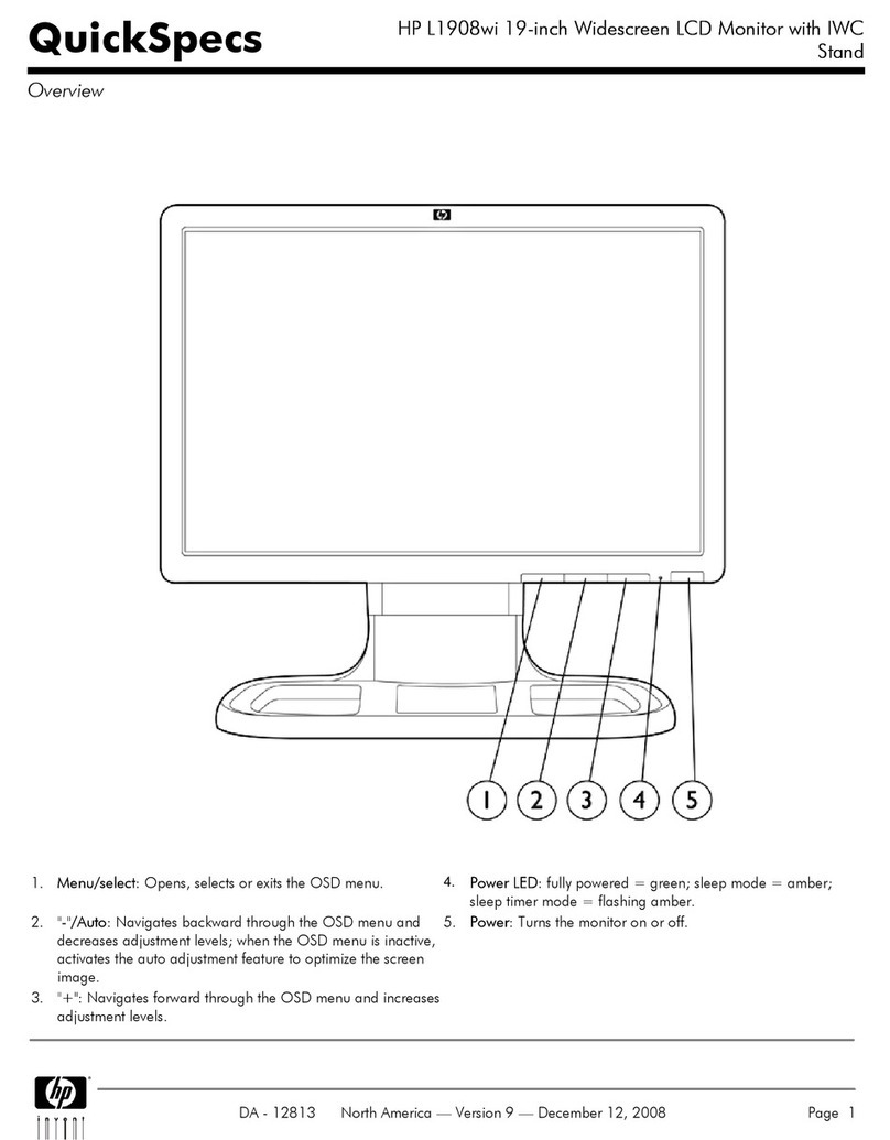
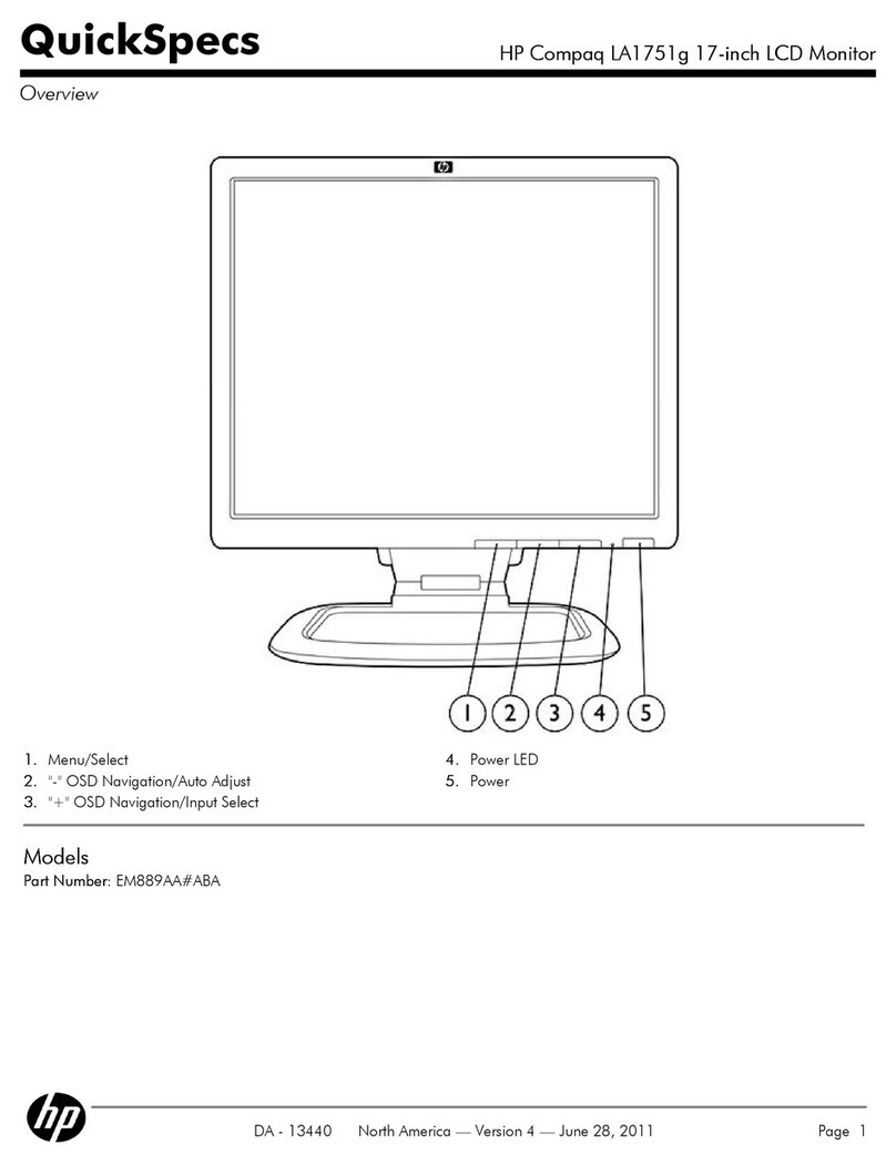
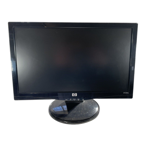
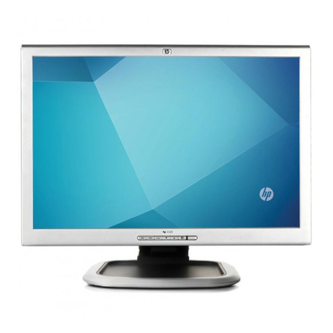
HP Pavilion F1723 User manual

ServiceManual
17-inch LCD Monitor
f1723/FP7317/L1702/vf17/FP17

Service Manual Versions and Revision
Copyright
Copyright 2003LiteOn Technology Corp.
All Rights Reserved
This manualmay not, inwholeorin part,becopied,
photocopied, reproduced, translated,orconvertedto any
electronicormachinereadable form without prior written
permissionof LiteOnTechnologyCorp.
f1723/ FP7317 / L1702 / vf17 / FP17 ServiceManual.
Trademarks
LiteOn is a registered trademarkof LiteOn
TechnologyCorp.
All other trademarks are the property of their
respective owners.
No.VersionReleaseDateRevision
1.1.0Feb.20,2003Originalrelease
2.2.0April 8,2003 Update

Page1
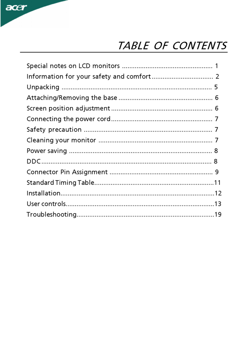
f1723/FP7317/L1702 /vf17/FP17
1)CircuitDescription
1.Audio circuit-------------------------------------------------------------------------------------------------------------------3
1.1 Audio input-----------------------------------------------------------------------------------------------------------------3
1.2 Audio output---------------------------------------------------------------------------------------------------------------3
2.Power supply-------------------------------------------------------------------------------------------------------------------3
3.Video inputcircuit-------------------------------------------------------------------------------------------------------------3
4.Definition converter LSIperipheral circuit---------------------------------------------------------------------------------3
5.Systemreset,LED control circuit--------------------------------------------------------------------------------------------3
6.E
2
PROM-------------------------------------------------------------------------------------------------------------------------4
7.Controllercircuit---------------------------------------------------------------------------------------------------------------4
7.1 Dection ofPOWER switch status---------------------------------------------------------------------------------------4
7.2 Display mode identification----------------------------------------------------------------------------------------------4
7.3 User control----------------------------------------------------------------------------------------------------------------6
7.4 Controlof identificationconverterLSI---------------------------------------------------------------------------------7
7.5 I2C bus control-------------------------------------------------------------------------------------------------------------7
7.6 Power ONsequence------------------------------------------------------------------------------------------------------8
7.7 Power OFF sequence-----------------------------------------------------------------------------------------------------9
7.8 List of CPU assignments-----------------------------------------------------------------------------------------------10
8Power Board Operation Therory----------------------------------------------------------------------------------------------11
9Inverter Circuit-------------------------------------------------------------------------------------------------------------------12

Page2
f1723/FP7317/L1702 /vf17/FP17
2)Trouble Shooting
1.Nodisplay of screen(Screenisblack,color of LED isamber)--------------------------------------------------------13
2.Nothing displayson screen(Screen is black, color ofLED is green)------------------------------------------------14
3.Checking the back lightunit-----------------------------------------------------------------------------------------------16
4.Abnormalscreen-------------------------------------------------------------------------------------------------------------17
5.No OSM display-------------------------------------------------------------------------------------------------------------18
6.Abnormal plug and playoperation---------------------------------------------------------------------------------------19
7.Checking the interface circuit ofsync signal----------------------------------------------------------------------------20
7.1 Checkingthe control circuit ofhorizontal sync pulse-------------------------------------------------------------20
7.2 Checking the control circuitof vertical sync pulse----------------------------------------------------------------20
8.Checking the resolution change IC movement--------------------------------------------------------------------------21
9.Checking theDC/DC converter circuit-----------------------------------------------------------------------------------22
10.Power board------------------------------------------------------------------------------------------------------------------23
3)RecommendedParts List
Recommended PartsList---------------------------------------------------------------------------------------------------24

Page3
f1723/FP7317/L1702 /vf17/FP17
1)CircuitDescription
1.Audio circuit (Circuit diagrams Main PWB5/5) (Optional)
1.1Audioinput
The audio signal input received from the audio input terminal (P305) is applied tothe amplifier I309 of 1 and 9
through the low-pass filterconsisting ofR361, R360, C370, C371, C361 andC363.
Inthisaudio circuit, controlsof Volume,and muteareconducted. Theaudio signalcontrolledbya VR determines
the attenuation of output of the amplifiers.
1.2Audio output
Theaudio signal is outputfromthe jackoutput terminal (P306) to the internal speaker system.
2. Interfaceboard and panelpowersupply(CircuitdaigramsMAIN PWB 2/5)
2.1P301 connector
A5V powersupply for LCDmodule, CPU,and logicis generated from theP301 connector.
2.2I301-pin 1:4-terminal regulator
A 3.3Vpowersupply for Scaler IC I304, is generatedfrom the5V source.
2.3I301-pin 1:5-terminalregulator
A 2.5V power supply for ScalerICI304 isgeneratedfromthe5V source.
Q302,Q303ON/OFFcontrol forLCD Module
ON/OFF control is performed for power ON/OFFand also for thepower saving sequence.
3.Video inputcircuit(Circuit diagramMAINPWB3/5)
Theanalog video signal inputentered from P302, theAC-coupled video signal is used to clamp the black levelat
0V).
4.DefinitionconverterLSIperipheral circuit (CircuitdiagramMAINPWB 4/5)
I304 gm2121 is thedefinitionconverter LSI.
The analog R, G,Bsignal input enteredfromthe video input circuitis convertedinto the digital dataof video
signal through theincorporated A/D converter. Based onthisconversion,thisdevice performs interpolation
duringpixel extension. The source voltage for thisdevice is 3.3V, 2.5V and the systemclockfrequencyis14.318
MHz. The withstandvoltage level for theinput signalvoltageofI304 is 3.3V and 5V.
5.Systemreset, LEDcontrolcircuit(CircuitdiagramMAIN PWB 4/5,2/5)
5.1System reset
System reset is performed bydetecting therising and falling ofthe 5Vsource voltageat I305.
5.2LED control circuit
Green /amberis lit with the controlsignal ofthe LEDGREEN andLEDAMBERsignal pin 34, 33 fromI304

Page4
f1723/FP7317/L1702 /vf17/FP17
6. E2PROM (Circuit diagramMAIN PWB 4/5)
Data transferbetween I307 (24LC16) andScallerIC I304 is effectedthrough theIICbus SCL(pin 37) andSDA(pin
36) of I304. The data to betransferred to eachdevice are stored in I307.
l I304 control data.
l OSD related setting data.
l Other control data forservice menu.
7.Controller circuit(Circuit diagramMAINPWB4/5)
ScallerIC I304 functions as theController.
Thesourcevoltagefor thedeviceare 3.3V and 2.5V and the system clockfrequencyis14.318MHz.
7.1Detection of POWER switch status
The CPU identifies the ON status of the twopower supplies. The identification is made when the power supply
isturned off. For example,ifthepower supply isturned off withthePOWER switch, thePOWER switchmustbe
turned onwhenactivating the powersupplyagain.Ifthe powersupplyisturnedoff bypulling outthepower
cord, thenthis power supplycanbe turned onbyconnectingthepower cord, withoutpressingthe POWER
switch.
7.2Display modeidentification
7.2.1Functions
(1)Displaymode identification
l The displaymode of input signal is identified basedon Table 1.
l When the mode has been identified through the measurement of horizontal and vertical frequencies, thetotal
number of lines is determined with a formula of Horizontalfrequency/ Vertical frequency= Totalnumber
of lines. Finalidentificationcanbe madebyexaminingthecoincidenceoftheobtained figure withthe
number oflines for the mode identifiedfromthe frequency. The boundary numberof linesin each modeis
shown in Table2.
l When the detected frequencyifthe sync signalhaschanged, the total number of lines should be counted even
though it is an identified frequencyin the same mode.
(2) Powersavemode.
The power save mode is assumed when the horizontal / vertical signals are as specified below.
l If there is no horizontalsync signal input.
l If there is no vertical sync signal input.
l If the horizontal syncsignal is outsidethe measuring range of gm2121.
l If the verticalsync signal is outside the measuring range of gm2121.

Page5
f1723/FP7317/L1702 /vf17/FP17
PolarityMode
ResolutionH-freq
(KHz)
BandWidth
(MHz) HV
1.VGA640 x480 60Hz31.47
25.175--
2.VESA640 X48072Hz37.86
31.5--
3.VESA640 X48075Hz37.531.5--
4.VGA720 x400 70Hz31.47
28.322-+
5.VESA800 x600 60Hz37.88
40 ++
6.VESA800 x600 72Hz48.08
50 ++
7.VESA800 x600 75Hz46.88
49.5++
8.MAC 832 x624 75Hz49.72
57.283--
9.VESA1024 x768 60Hz48.36
65 --
10.VESA1024 x768 70Hz56.48
75 --
11.VESA1024 x768 75Hz60.02
78.75 ++
12.MAC 1152 x87075Hz68.68
100 --
13.SUN 1152x90 76Hz71.71
105.6--
14.SXGA1280 x102460Hz64 108 ++
15.SXGA1280 x102475Hz80 135 ++
Table 1

Page6
f1723/FP7317/L1702 /vf17/FP17
7.3User Control
7.3.1Related ports andpinof I304
IndicationresolutionThe numberofthe
distinctionlines
DistinctionVsync
640 x480487 <LINE < 607fV< 63Hz
63 Hz<fV< 68Hz
68 Hz<fV< 74Hz
74 Hz<fV< 78Hz
800 x600607 <LINE < 777fV< 58Hz
58 Hz<fV< 63Hz
63 Hz<fV< 73Hz
73 Hz<fV< 78Hz
832 x624640< LINE -
1024 x768 768 <LINE < 870fV< 63Hz
68 Hz<fV< 73Hz
73 Hz<fV< 78Hz
1152x864 870 <LINE< 1031
1280 x960 960 <LINE< 1027
1280 x1024 1027 <LINE
7.3.2Functions
Controlis effected for the push-switches to be used when the user changes the parameters, in order to modify the
respective setting values.Whether the switchhasbeenpressedisidentifiedwith theswitch inputlevel that is
turned L”.
Each switch input port is pulled up atoutside of ASIC
Each parameter is stored in the EEPROM,the contents of which areupdatedas required.
.
Port Pin No. I/O
Signal name
Function Remarks
GPIO3 I304, 26
IMENU EXIT/ENTER switch input
GPIO7 I304, 32
IMINUS switch input Auto-Adj.
GPIO6 I304, 29
IPLUS switch input
GPIO21
I304, 16
IPOWER soft power switch input
Table 2 the number of the lines, Vsync distinction

Page7
f1723/FP7317/L1702 /vf17/FP17
7.4Control of definition converter LSI
7.4.1Functions
Major function of I304 are as follows:
(1)Expansion of the displayscreen.
(2)Timing control for various signal types.
(3) Power-supply sequence(LCDpanel).
7.5I
2
C bus control
7.5.1I
2
C-controlled functions
Thefollowing functional controls are effected by I2C.
(1) ControlofEEPROMI307 for parametersetting.
(2) Control ofaudio preamplifier.

Page8
f1723/FP7317/L1702 /vf17/FP17
7.6Power ONsequence
When the POWER switch is pressed, thePOWER signal is turned L”. When this L”potential is detected, the
CPUbegins toestablish the respective powersuppliesaccording to the sequence shownbelow.
AB
Panel-AU 0msmin250 msmin
Panel-HD 20~50 ms500 msmin
Panel-LG 0.01~50 ms200 msmin
Panel_VCC
Backlight
Panel_DATA

Page9
f1723/FP7317/L1702 /vf17/FP17
7.7Power OFF sequence
When thePOWER switch is pressed while the power supplyis ON, the POWER signal is turned L”. When this
L”potentialis detected,theCPU begins to turn off therespective powersuppliesaccording to the sequence
shownbelow.
CD
Panel-AU 0msmin0msmin
Panel-HD 0~50 ms100 msmin
Panel-LG 0.01~50 ms200 msmin
Panel_VCC
Backlight
Panel_DATA

Page 10
f1723/FP7317/L1702 /vf17/FP17
7.8Listof GPIO PinAssignmentsofthe I304
PortPin No.
Signal NameInitial Setting
Function Remark
GPIO1
24 MUTEHAudio Mute Enable
GPIO21
16 KEY_POWER
HON/OFF Monitor Power
GPIO4
27 UART_DIHUARTinterface data IN
GPIO5
28 UART_DO HUARTinterface data OUT
GPIO13
37 NVRAM_SCL
HNVRAM_SCL
GPIO12
36 NVRAM_SDA
HNVRAM_SDA
GPIO9
33 LED_AMBER
LLED_AMBER Enable
GPIO10
34 LED_GRNHLED_GRNEnable
GPIO7
32 KEY_MINUSHKEY_LEFTEnable
GPIO0
23 BKLT-ADJ-Backlight Brightness Control
GPIO11
35 WRn-Flash RomWrite Enable
GPIO18
12 A16 -Address Input
GPIO19
11 A17 -Address Input
GPIO26
29 KEY_PLUSHKEY_RIGHT
PBIAS
41 BKLT_ENHBacklight_Enable
PPWR 40 PANEL_ENHPanel_Vcc Enable

Page 11
f1723/FP7317/L1702 /vf17/FP17
8. Power Board Operation Therory
8.1Line filterconsists ofC801, T801, C802, C803, C804, C837, C838. Iteliminates highfrequency interferencetomeet
EMI’srequirement.
8.2Rec &Filter
Bridgediode D801 convertsAC sourceinto pulsed DC. This pulsed DCis smoothed andfiltered by C805. R802 is
an NTC ( negative thermal coefficient ) resistor, used to reduce inrushcurrent to be within safe range.
8.3Powertransformer:
T802 converts energy for squarewavefrompowersourceC805 to secondarysideto generate +12V and+22.5V.
8.4Output :
The squarewave fromT802 is rectifiedbyD809, D810, then filteredbyC817, C822togenerate +22.5Vand+12V
respectively.
8.5Driver:
Q803 drive T802 fromPWM controlofI801 for power converted.
8.6FB:
Negativefeedback CKTconsists of photo coupler I802 and adjustable regulator I803. It can maintain output
voltages +22.5Vand +12Vat astable level.
8.7PWM :
8.7.1Start: Whenpower is turned on.C807 is charged a 15 volt and a starting current above 40uA to pin7 of I801.
I801 starts to oscillate and outputs a pulse train through pin 6 to drive Q803.
8.7.2OPP:When Q803 turns on, C805 supplies alinearlyincreasingtrianglecurrent through the primaryinduc-
tance of T802 to the driver Q803, once the peak value of this current multiplied byR811 exceeds1 volt,
pulsetrain will be turn off immediately toprotectQ803, T802 from beingburnedout.
8.7.3Regulation: If output voltage +22.5V goes up, theR terminal of I803 getsmorebias, accordingly photo
transistor and photo diode flows more current. The voltage of pin 2 goes up too, making the pulse width of
pin 6 to becomenarrower. So the output voltage +22.5V willbe pulled down to a stablevalue.
8.7.4OVP: If +22.5V goesup too much, the induced voltageonpin 4of T802 becomes largealso. Supposethatit
isover 18 volts, ZD801 conducts, pin3 of I801 ispulled up over 1 volt. The pulse train atpin 6 goes downto
zero, shuttingQ803 offimmediately.
8.7.5SCP: If output terminal isshort to ground, photo transistor does not conduct, hence Q806 does not conduct
either. Then oscillation of I801 is stop, shutting Q803 off immediately.
Line
Filter
Rec. &
Filter Power
Transformer OutpurRec. & Filter
PWM Driver
FB
HPD-K17AA Power Board Block Diagram

Page 12
f1723/FP7317/L1702 /vf17/FP17
9. Inverter Circuit
This unit operates on an output voltage of 15Vfrompower source.
9.1Regulator:Q101 get a+5VDC for I101 powersupply.
9.2UVP: Q106 turnsoffwhen theVinisunder 10V.Then pin3of I101 is pulledlow andinverteroff immediately.
That is the undervoltage protection.
9.3Control IC: I101 (OZ960S)
9.3.1Enable :When pin 3ofI101 is over1.5V,I101 works.Ifitis under1.5V,I101 turns off.
9.3.2OSC:WhenI101 enabled, R108/C115 (pin17/pin18 ofI101) determinethe operating frequency.
9.3.3SST: C104 (pin 4of I101) provides soft start function.
9.3.4Ignition: R109 (pin 8 of I101) provides higher operating frequencyfor more striking voltage until regulation of
feedback of lampcurrent. C103 (pin 1ofI101) determine the striking time.
9.3.5Dimming control:The divided voltage of R106/R105/R104 control the dutypulse of burst-mode to drive Q105
andperform awidedimming control for theCCFL. Theburst-mode frequency is determinedby C116.
9.3.6Regulation: Pin 9/pin 10 ofI101 provideregulationoftheCCFL current fromfeedback.The non-inverting reference
(pin10of I101)is at1.25V nominal.
9.3.7Protection:Open-lamp protection in the ignition period isprovided through bothpin1 and pin2 of I101.
Removalof the CCFLduringnormaloperation willtriggerQ107 toturnson andshutsofftheinverter.Thisislatch
function.
9.3.8Outputdrivers: Theconfiguration prevents anyshoot-through issue associated with bridge-type power
conversionapplications.Adjusting the overlapconductionbetween I102 P-MOSFET andI103 N-MOSFET,I102 N-
MOSFET and I103 P-MOSFET,theCCFLcurrentregulation is achieved, sameasI104 andI105.
9.4Full-bridge swit ching/Transformer:I102/I103/C123/I104/I105/C137/T101/T102 compose full-bridge swit ching to
convertDC intoACfor driverthe CCFL.
9.5Detection: C128/C129/C130/C131/C132/C133 detect theoutput voltage andensurearatedvoltagebypin2of I101/
Q108/Q109 ensurenotaopen-lamp.
9.6Feedback:D116/D117/D122/D123/D109/R120/R121/D108 sense thelamp currentfornegative feedbackand
regulation.
Inverter Board Block Diagram
VCC
Regulator
U.V.P. Enable
OSC
SST
Dimming
control
Output driver
Protection
Ignition
Regulation
Control IC : OZ960
ON / OFF
Full-bridge switching Transformer Lamp
Feed back
Detection
Brightness
control
VDD

Page 13
f1723/FP7317/L1702 /vf17/FP17
2) Trouble Shooting
1. Nodisplay of screen (Screen isblack,colorofLEDis amber)
Does OSM display when you push
MENU button.
Yes
Check ifthe sync signal from Computer
is output and if the video cable is
connected normally.
No Preceed "Nothing displays on
screen"section.
OK
Proceed "Checking the resolution change
IC movement" section.
NG Input the sync signal of computer, or
change the cable.
When a signal isn't
being inputted, it is
indicated with "VIDEO
INPUT". It is indicated
with "OUT OF RANGE"
at the time of the
frequency that it can't be
distinguished.

Page 14
f1723/FP7317/L1702 /vf17/FP17
2. Nothing displays on screen (Screen is black,colorof LEDis green)
Is backlight lit?
OK
Does computer output RGB video signals?
NG Refer "Checking the backlight unit" section
OK
Check OSM menu is displayed on screen
when you push the "MENU" key.
NG
1) Change pattern of video signal output on the
host.
2) Reconnect the video cable.
3) Change the video cable.
OK NG
Proceed "Abnormal screen" section.
Check if the signal cableis connected between the
MAIN PWB and LCD module.
OK
NG
Next Page
Failure Point
The Cable is disconnected.

Page 15
f1723/FP7317/L1702 /vf17/FP17
Continue
Check if the voltage on I301 pin 1 that
is high level DC at 5V.
Check the 3.3 V power are supplied on I301, pin 4.
OK
NG
OK NG
Failure point
1) Printed wire broke between P301 pin 7, 8 and
and I301.
2) Check power board.
Failure point
I301 Failure
Failure point
1) The cable broke between P303 and LCD
module.
2) LCD module failure.

Page 16
f1723/FP7317/L1702 /vf17/FP17
3. Checkingtheback lightunit
Is +22.5V supplied to inverter PWB?
OK NG
Failure point
1) Inverter cable disconnection.
2) Power board failure.
Check the BKLT_EN signal of the rectangle input P301 pin 2 at TTL high level
OK
NG Is a "H" level being output in the TTL level from I304 pin 41
Or, is BKLT_EN signal of the rectangle beingoutput?
NG
Failure point
Printed wire broke between
I304 pin 41 and R387.
Check the PWM signal of the input from I304 pin 23 is a PWM signal.
OK
NG
Failure point
1) Printed wire broke between
I304 pin 23 and R301.
2) I304 failure.
Failure point
1) Inverter cable disconnection.
2) Inverter of LCD module failure.

Page 17
f1723/FP7317/L1702 /vf17/FP17
OK NG
Failure point
1)No R, G andB video signal output from host computer. Check
computer
2)Videosignal cabledisconnection.
OK
NG
Check the R, G, B videosignal from computer input on
D-Sub R, G, B connector.
Check the R, G, B input signalson I304 pin135, 131, 127
respectively that their level is0.7Vp-p maximum.
Failure point
In thecase of theRedsignal. (A Green and Bluesignal is the same
path, too.)
1)Printedwirebroke between D-Sub(R)and I304pin 135.
2)R323short.
3)C317open.
4)R321open.
Check thehorizontal sync pulse
input to I304 pin101at TTLlevel.
OK NG
Failure point
1)Printedwirebroke between I304 pin101andP302 pin8.
2)I304failure
Check thevertical sync pulse
input to I304 pin100at TTLlevel.
OK NG
Process "Checking the resolutionchange ICmovement"
section.
Failure point
1)Printedwirebroke between I304 pin100andP302 pin9.
2)I304failure
4. Abnormalscreen

Page 18
f1723/FP7317/L1702 /vf17/FP17
5. NoOSMdisplay
OK
NG
Check the input TTL level whether was changed when pressed function keys.
Failure point
1) Printed wire broke between P308 pin 5 and I304 pin 29.
2) Printed wire broke between P308 pin 6 and I304 pin 32.
3) Printed wire broke between P308 pin 7 and I304 pin 22.
4) Printed wire broke between P308 pin 8 and I304 pin 26.
5) Printed wire broke between P308 pin 4 and I304 pin 16.
6) FB325, FB326, FB327, FB328. FB329 open
7) RN302, RN301, short/open.
8) I304 failure.
Proceed "Checking the resolution change IC movement" section.
This manual suits for next models
4
Table of contents
Other HP Monitor manuals

HP
HP HP 71 Instruction manual

HP
HP Z24i User manual

HP
HP D5063H - Pavilion F50 - 15" LCD Monitor Installation and operating manual

HP
HP Compaq LE19f User manual

HP
HP 55HP User manual

HP
HP 2509m Assembly instructions

HP
HP EliteDisplay E221c Installation guide

HP
HP Pavilion 27q Installation instructions

HP
HP ProDisplay P17A LED Backlit User manual

HP
HP P22v G5 Manual