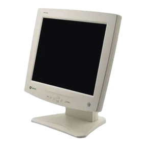
HP R15AAC User manual

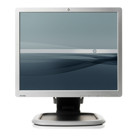
15-inch LCD Monitor
R15AAC/AAU (vs15)
ServiceManual

Service Manual Versions and Revision
Copyright
Copyright 2004LiteOn Technology Corp.
All Rights Reserved
This manual maynot,in wholeorin part,be
copied,photocopied, reproduced, translated, or
converted to anyelectronic or machine readable
formwithout prior written permission of LiteOn
TechnologyCorp.
HPHPD_R15AAC/AAU(vs15)ServiceManual.
PrintedinTaiwan.
Trademarks
LiteOn is a registered trademark of LiteOn
Technology Corp.
All other trademarks are the property of their
respectiveowners.
No.VersionReleaseDateRevision
1.1.0Dec. 10,2004Originalrelease

Page2
R15AAC/AAU (vs15)
1)PowerBoardOperationTherory
1.Theroryof PowerBoard Operation-----------------------------------------------------------------------------------------4
2)InverterCircuit
2.InverterCircuit-----------------------------------------------------------------------------------------------------------------5
3)Interface Operation
3.1Top---------------------------------------------------------------------------------------------------------------------------6
3.2Power------------------------------------------------------------------------------------------------------------------------6
3.3VGA&DDCinterface-----------------------------------------------------------------------------------------------------6
3.4ScalerGM5321-------------------------------------------------------------------------------------------------------------7
3.5 Key &Panelinterface-----------------------------------------------------------------------------------------------------8
3.6Audio------------------------------------------------------------------------------------------------------------------------9
3.7 Others---------------------------------------------------------------------------------------------------------------------10
3.7.1Detection of POWERswitch status--------------------------------------------------------------------------------10
3.7.2 Displaymodeidentification------------------------------------------------------------------------------------------10
3.7.3 ListofI/OPinAssignments of theI311----------------------------------------------------------------------------12
4)TroubleShooting
1.For PowerBoard-------------------------------------------------------------------------------------------------------------13
2.For Inverter Board-----------------------------------------------------------------------------------------------------------14
3.Nodisplay of screen(Screenisblack,color of LED isamber)--------------------------------------------------------15
4.Nothing displayson screen(Screen is black, color ofLED is green)------------------------------------------------16
5.Checking the back lightunit-----------------------------------------------------------------------------------------------18
6.Abnormalscreen-------------------------------------------------------------------------------------------------------------19
6.1Abnormalscreen for VGAsource-------------------------------------------------------------------------------------19
7.Abnormal OSMdisplayadjust problem----------------------------------------------------------------------------------20
8.Abnormal plug and playoperation---------------------------------------------------------------------------------------21
8.1Abnormalplugandplay operation for VGA-------------------------------------------------------------------------21

Page3
R15AAC/AAU (vs15)
9.Checking the interface circuit ofsync signal----------------------------------------------------------------------------22
9.1 Checking thecontrol circuit of horizontal syncpulsefor VGA--------------------------------------------------22
9.2 Checking the controlcircuit ofvertical sync pulseVGA----------------------------------------------------------22
10.Checking the resolution change IC movement--------------------------------------------------------------------------23
11.Audio no signal output-----------------------------------------------------------------------------------------------------24
5)Spare Parts
RecommendedSpare PartsList-------------------------------------------------------------------------------------------------26
6)BlockDiagram
Blockdiagram----------------------------------------------------------------------------------------------------------------------27

Page4
R15AAC/AAU (vs15)
1).PowerBoardOperationTherory
1.1LinefilterconsistsofC801,T801,C802,C803, C804,C809,C815,C838,R801.It eliminateshighfrequencyinterference
tomeetEMI s requirement.
1.2Rec &Filter
Bridgediode D801 convertsAC sourceinto pulsed DC. This pulsed DCis smoothed andfiltered by C805. R802 is
an NTC ( negative thermal coefficient ) resistor, used to reduce inrushcurrent to be within safe range.
1.3Powertransformer:
T802 converts energy for squarewave frompower sourceC805 to secondaryside to generate+5V, +12V and
+21.5V.
1.4Output :
Thesquare wavefromT802 is rectified by D808D809,D810,then filteredbyC818,C824,C829, C813,C822 to
generate +21.5Vand+12V,+5Vrespectively.
1.5Driver:
Q803 drive T802 fromPWM controlofI801 for power converted.
1.6FB:
Negativefeedback CKTconsists of photo coupler I802 and adjustable regulator I803. It can maintain output
voltages +21.5Vand+12V, +5Vat astable level.
1.7PWM :
1.7.1Start :Whenpower isturnedon. C807 ischarged a 12 voltanda starting currentabove1mA to pin1 of I801.
I801 starts to oscillate and outputs a pulse train through pin 6 to drive Q803.
1.7.2OPP:When Q803 turns on, C805 supplies alinearlyincreasingtrianglecurrent through the primaryinduc-
tanceof T802 tothedriver Q803, oncethepeak valueofthiscurrentmultiplied byR811 exceeds1volt, pulse
trainwill beturnoff immediately toprotectQ803, T802 from being burnedout.
1.7.3Regulation: If output voltage +21.5V goes up, theR terminal of I803 getsmorebias, accordingly photo
transistor and photo diode flows more current. The voltage of pin 2 goes up too, making the pulse width of
pin 6 to becomenarrower. So the output voltage +21.5V willbe pulled down to a stablevalue.
1.7.4OVP: If +21.5V goesup too much, the induced voltageonpin 4of T802 becomes largealso. Supposethatit
isover 18 volts. The pulse train at pin 6 goes down to zero, shutting Q803 off immediately.
1.7.5SCP: If output terminal isshort to ground, photo transistor does not conduct, hence Q807 does not conduct
either. Thenoscillation of I801 is stop, shuttingQ803 off immediately.
Line
Filter Rec. &
Filter Power
Transformer Outpur Rec. &Filter
PWM Driver
FB
Power Board Block Diagram
Page5
R15AAC/AAU (vs15)
2)InverterCircuit
This unit operates on anoutput voltage of 21.5Vfrompower source.
2.1VDD:R105 get a+5VDC forI101 powersupply.
2.2ControlIC:I101(OZ9930)
2.2.1Enable :When pin1ofI101 is over0.55V,I101 works.Ifit is under0.55V,I101 turns off.
2.2.2OSC:WhenI101 enabled, C104/C105 (pin 2ofI101) determine the operating frequency.
2.2.3SST: C106 (pin 1of I101) provides soft start function.
2.2.4Ignition:ICprovideshigher operatingfrequency internally for morestrikingvoltage untilregulationoffeedback of
lamp current.And provide 2 sec strikingtime.
2.2.5Dimming control: Thedividedvoltageof R106/R103/R104control the duty pulseof burst-mode to driveand
performawidedimming controlfor theCCFL.Theburst-modefrequencyis determinedbyoperating freq/233.
2.2.6Regulation:Pin 8of I101 provideregulation of theCCFLcurrent fromfeedback.Thenon-invertingreferenceis at
1.25Vnominal.
2.2.7Protection: Open-lamp protection in the ignition period is provided throughpin 7 of I101.
Removal of the CCFLduring normal operation will trigger IC to turns on and shuts off the inverter. This is latch
function.
2.2.8Outputdrivers: Theconfiguration prevents anyshoot-through issue associated with bridge-type power
conversionapplications.Adjusting the overlapconductionbetween Q104, the CCFLcurrent regulation is achieved.
2.3Half-bridgeswitching/Transformer: Q104, C122, C123 composehalf-bridgeswitchingtoconvertDC intoACfor
drivertheCCFL.
2.4Detection: C132, C112, C114, C126, R116, R115, C115 detect the output voltage andensure aratedvoltagebypin7
ofI101 ensure not aopen-lamp.
2.5Feedback:D116,D117, R111, R112, C109 sensethelampcurrentfor negativefeedback andregulation.
Inverter Board Block Diagram

VCC
VDD
Enable
OSC
SST
Outputdriver
Protection
Ignition
Regulation
Control IC : OZ9930
ON / OFF
Halfl-bridgeswitching
Transformer
Lamp
Feed back
Detection
VDD
Dimming Control
Brightness
Control

Page6
R15AAC/AAU (vs15)
3)InterfaceOperation
3.1Top(Circuit diagramssheet2of 8)
Thispage isfunctionblock.(1)Power.(2)VGA&DDCinterface. (3) ScalerGM2621.
(4) Key&panelinterface.(5)Audio
3.2Power(Circuit diagramssheet 3of7)
3.2.1P301 connector
A5Vpower supplyforflashROM,EEPROMofEDID, logic.Itisgeneratedfrom the
P301 connector.
3.2.2I304:3-terminalregulator
A3.3V power supplyforI307scaler ICgm2621LCDmodule, itisgenerated from the 5V
source.
3.2.3I305:3-terminalregulator
A1.8V powersupplyfor I307 scalerICgm2621, itisgenerated from the3.3Vsource
(I304).
3.2.4Q302, I301 :ON/OFF controlfor LCDmodulepower
ON/OFF control(PANELVCC_EN) is performedforpower ON/OFFand also for the
power saving sequence. Itissupport3.3V toLCDmodulepower.The PANELVCC_EN
signalisgenerated from I307scalerICgm2621.
3.2.5R305: ON/OFFcontrolfor LCDmodulebacklightpower
ON/OFF control(BKLT_EN) isperformed for blacklightpowerON/OFF and also for
thepower savingsequence. TheBKLT_ENsignal isgeneration from I307scalerIC
gm2621.
3.2.6Q301:Adjustbacklightluminance forLCDmodule
Itisadjustedback lightluminancecontrol (BKLT_ADJ)is performedforthe backlight
luminance.The BKLT_ADJsignal is generatedfrom I307scalerICgm2621.
3.3VGA&DDCinterface(Circuitdiagramssheet4of 7)
Thissheet haveRGBanalogvideosignals inputfromVGAconnector.Select H/Vsyncsignals
sourcefromVGAconnector.
TheRGBanalogvideosignals inputthroughAC-coupled,analogvideo signalisusedto clampthe
black levelat0V.And H/V sync tosclaer.
AndsupportDDC plug&playfunctionforanalogvideo.
3.3.1P302 connector
TheRGB analogvideoinput signals fromthe P302connector.
3.3.2I306DDCEEPROM
ThisICissupportDDC2Bofthe VESAstandard, also plug and playfor the PC host.

Page7
R15AAC/AAU (vs15)
3.4Scaler gm2621(Circuitdiagrams sheet 5of 7)
TheI307gm2621isall-in-oneLCDmonitor controller.Thegm2621 leveragesGenesispatented
advancedimage-processingtechnologyaswellasaprovenintegratedADC/PLL.Gm2621 also
integrates amicro-controller,anOSDcontroller,anddual LVDS.
TheRGB analogvideosignalinputenteredfromthevideoinputcircuitisconvertedintothedigital
dataofanalogvideosignalthroughthe incorporatedA/Dconverter.
Basedonthisconversion,thisdeviceperformsinterpolationduringpixelextension.Theseinterpo-
lation digital data aretransformedtoLVDSsignal.The I307source voltageis3.3V and1.8V,the
device clocksource frequencyis14.318MHz.Andsupportkeypadfunction.
3.4.1I310 SPIFlash ROM
Thefirmwareprogramrunningfrom I310external ROM,containsfirmware codeanddata
forall firmwarefunction,andcontroldata andparameter andOSD relatedsetting and other
servicedata.The deviceis8bitconfiguration,1024Kbytes of ROM.
3.4.2I308MicroprocessorSupervisoryCircuit
The function of thisdeviceistoassertaresetto I307scalergm2621,if either the power
supplydropped down.
3.4.3X30114.318MHz
Itgenerated reference clockinputforI311scaler.
3.4.4ISPandDDC2Bifunction
TheDDC2BiisVESAstandardforthe hostPC system,itcanthroughDDC2Bibuscontrol
LCDmonitor.Enter I307 pin54DDC_SCLandpin55DDC_SDAofthe VGAport.
ItuseISP functionwhen change new firmware toI310flashROM.ItusedDDC2B port
IICbus through I307gm2621toI310 flash ROM.
3.4.5Thepowersavesequence function
FirstdisableI307pin49(BKLT_EN)fromHto Lof LCDmoduleback lightpower,delay
sometime,then disable I307 pin127(PANELVCC_EN)fromHto LofLCDmodule
power, then I307 entertopower downmode.

Page8
R15AAC/AAU (vs15)
3.5Key&Panelinterface(Circuit diagramssheet6of 7)
3.5.1P306 connector
ItisLVDSbus, it isfromI307scaler toLCDpanel module.The outputvoltageis3.3V.
3.5.2P307 connector
TheP307 hassupportkeypadfunction.Controlisgiveeffect to for the pushswitchtobe
used whenthe user changestheparameters,inorderto modifythe respectivesetting values.
Whethertheswitch hasbeenpressedis identifiedwiththe switchinputlevelthat inputsa
DCvoltage intoI107pin113 (LBADC_IN3) andpin114 (LBAD1_IN2).
Eachswitch input voltagebasedonTable 1.
Each parameterisstored inthe I310EEPROM, the contentsofwhichare updatedas
required.
TheP307have LEDBlue andAmber light,the LEDBlue signal fromI307 pin51,and the
LEDAmbersignal from I307pin 56.
Table 1Related portsof I311
PinNo.
I/O
Signal nameFunctionRemarksVoltage
Pin114
IKEY_POWER
Soft power switch
input
Power key1.05V
LBADC_
IN2 Pin114
IKEY_MENU
Enter OSDswitch
input
Enter OSDmenu
1.69V
Pin113
IKEY_UPswitchinputUpkeyor
Source2
2.3V
Pin113
IKEY_DOWN
switchinputDownkeyor
Source1
1.9V
LBADC_
IN3
Pin113
IKEY_SELECT
Selectionswitch
input
Select keyor
Autoadjust key
1.57V
↓

Page9
R15AAC/AAU (vs15)
3.6Audio(Circuitdiagramssheet 7of7)
3.6.1P307 connector
TheP307 isaudio signalinput from thekeypadfunctionboard.
3.6.2P308 connector
TheP308 havetwo audiofunctionsignals.One isaudiovolume controlfrom thekeypad
functionboard. Other isaudiooutputtospeaker or earphone-jack.
3.6.3I312TDA74965A
TheI312 is5x5Wstereoaudioamplifier,it isanintegratedclass-B dualoutput amplifier.
3.6.4Q308, I313:ON/OFFcontrolforAudiopower
ON/OFF control(AUDIO_PW)isperformed for power ON/OFF andalso for theaudio
powerdown sequence. Itissupport12V toaudiopower.TheAUDIO_PWsignalis
generated fromI307 scaler ICgm2621.
3.6.5R385,Q309:MUTE control forAudio
MUTEcontrol (MUTE) isperformed foraudio returntomute andalsoforthe audio power
down sequence. TheMUTEsignalisgeneratedfrom I307scalerICgm2621.

Page 10
R15AAC/AAU (vs15)
3.7Others
3.7.1DetectionofPOWERswitchstatus
TheI307gm2621identifiesthe ON statusofthe twopower supplies. The identificationis
madewhenthepower supplyis turn off.Forexample, if the powersupplyisturn offwith
thePOWER switch,the POWERswitch mustbeturn onwhenactive thepowersupply
again.Ifthepower supplyisturned off by pullingout thepower cord, then this power
supplycanbeturnedonbyconnectingthe power cord,without pressing the POWER
switch.
3.7.2Displaymodeidentification
3.7.2.1Displaymodeidentification
Thedisplaymodeof inputsignal isidentifiedbased onTable 2.
Whenthemodehasbeenidentifiedthroughthemeasurementof horizontaland
verticalfrequencies,thetotalnumberoflinesisdeterminedwithaformulaof“Hori-
zontalfrequency/Verticalfrequency=Totalnumberofnumberof lines”.Final
identificationcanbemadebyexaminingthecoincidenceoftheobtainedfigurewith
thenumberoflinesforthemodeidentifiedfromthefrequency.TheDistinction
HsyncandVsync ofeachmode isshowninTable3.
Whenthe detected frequencyifthe syncsignal haschanged,the totalnumber of
linesshouldbecountedeven throughitisrangeidentifiedfrequencyinthesame
mode.
3.7.2.2Out ofrange
Thisout ofrange modeis assumedwhenthe frequencyoutof thehorizontal /
verticalsignalisasspecifiedbelow.
Vertical frequency :56~76Hz.
Horizontalfrequency:30~63KHz.
3.7.2.3Power save mode
Thepower save modeisassumedwhen thehorizontal/verticalsignals areas
specifiedbelow.
Ifthereisnohorizontalsyncsignalinput.
Ifthereisnoverticalsyncsignalinput.
Ifthehorizontalsyncsignal isoutsidethe measuringrangeofI307 gm2621.
Iftheverticalsync signalis outsidethemeasuringrange ofI307gm2621.
●
●
●
●
●
●
●
●
●

Page 11
R15AAC/AAU (vs15)
PolarityMode
ResolutionH-Freq
(KHz)
Band Width
(MHz) HV
1640x480(59.94Hz)31.46925.175 --
2640x480(72Hz)37.86131.5--
3640x480(75Hz)37.531.5--
4720x400(70Hz)31.46928.322 -+
5800x600(60Hz)37.87940 ++
6800x600(72Hz)48.07750 ++
7800x600(75Hz)46.87549.5++
8832x624(74.55Hz)49.72257.28--
91024x768 (60Hz) 48.36365 --
10 1024x768 (75Hz) 60.02378.75++
111152x870 (75Hz) 68.68 100+/- +/-
12 1152x900 (76Hz) 71.71 105.6 --
13 1280x960 (60Hz) 60 108+/- +/-
14 1280x1024 (60Hz) 63.981108++
15 1280x1024 (75Hz) 79.976135++
Table2video mode
Table3theHsync,Vsyncdistinction
Indication
resolution
Distinction HsyncDistinction Vsync The fixed
mode
720 x400 30.5KHz≦fH≦32.5KHz69Hz≦fV≦71Hz 4
640 x480 30.5KHz≦fH≦32.5KHz59Hz≦fV≦61Hz 1
36.9KHz≦fH≦38.9KHz71.8Hz≦fV≦73.8Hz
2
36.5KHz≦fH≦38.5KHz74Hz≦fV≦76Hz 3
800 x600 36.9KHz≦fH≦38.9KHz59.3Hz≦fV≦61.3Hz
5
47.1KHz≦fH≦49.1KHz71.2Hz≦fV≦73.2Hz
6
45.9KHz≦fH≦47.9KHz74Hz≦fV≦76Hz 7
832 x624 48.7KHz≦fH≦50.7KHz73.5Hz≦fV≦75.5Hz
8
1024 x768
47.4KHz≦fH≦49.4KHz59Hz≦fV≦61Hz 9
59KHz≦fH≦61KHz 74Hz≦fV≦76Hz 10
1152 x870
67.7KHz≦fH≦69.7KHz74Hz≦fV≦76Hz 11
1152 x900
70.7KHz≦fH≦72.7KHz75Hz≦fV≦77Hz 12
1280 x960
59KHz≦fH≦61KHz 59Hz≦fV≦61Hz 13
1280 x1024
62.9KHz≦fH≦64.9KHz59Hz≦fV≦61Hz 14
1280 x1024
79KHz≦fH≦81KHz 74Hz≦fV≦76Hz 15

Page 12
R15AAC/AAU (vs15)
3.7.3ListofI/O PinAssignmentsofthe I311
Pin No.
Port Signal Name Initial
Setting
Function
51GPIO0LED_BLLEDgreen enable
56GPIO1LED_ALLEDamber enable
50GPO4
BKLT_ADJ
-Backlight brightness control
57GPO2MUTELMute Audio
58GPO3AUDIO_PW LON/OFF Audio power
115LBADC_IN1
VGA_DETn HVGAcable connected
127PPWR PANELVCC_EN LPanel powerenable
49PBIAS BKLT_ENLBack light power enable

Page 13
R15AAC/AAU (vs15)
3)Troubleshooting
1.For PowerBoard
Checkoutput voltage +5V,+12V,+21.5V are right or not
NG OK It is not power boardproblem
Check power switchis turn onor not
OK NG Turn switch on
Check power cord (P801),signal cable (P302), P802,P101, P102, P103,
P104 is connectedright ornot
OK NG
Check C805is about DC140V-330Vor not
OK NG
CheckC807 is over 11V or not
OK NG
Connect it right
CheckF801,D801,P801 andrepair them
Check pin6 of I801have same pulse or not
OK NG
Check pin1 ofT802have same pulse or not
OK NG
Checkperipheral component of I801 andrepair them
Check L805,D804, I801and repair them
Check peakvoltage of R811 triangle pulse isup to1volt or not
OK NG
Check D809, D810, D811,C818. C829, C813, C824, C822, T802have
same short circuit or the output +5V, +12V, +21.5V is over load
OK NG
Check feedback circuit around I802, I803 andthe othercomponents and
repair them
Repair them
Check D804, L805 andrepair them
CheckQ803,R813, R814,D806,R811, R815 andrepair them

Page 14
R15AAC/AAU (vs15)
2.ForInverterCircuiton PowerBoard
Check C102 pin is around 5V.
On/Off pin of P802 isover 2V.
Brightness pinis between 0V and 3.5V/
OK NG Itisnot inverter problem
Check pin6 of I101 is 5V
OK NG Check R105, C102 and repairthem. Check printed wire.
Check P101, P102, D103 are connected right
OK NG
Check pin7 of I101 is over 3.1V
OK NG
Check pin2 of I101 is triangle pulse
OK NG
Check CCFL and repairthem. Lock P101, P102 tightly
Check Q106, Q107 and repairthem
Check pin 1of I101, there issoft start edge up to4V and pin 4, 5. there
is some pulse outputs
OK NG
Check pin 6 ofI101, there is around 1.25V from output detection
OK NG
RepairI101
Check C104, C105, I101 and repair them
Check SW MCS (Q104) workright
OK NG
Check trabsfirner (T101) working itand repair it
Repairthem
Check D116, D117, R111 and repairthem

Page 15
R15AAC/AAU (vs15)
3.No displayofscreen (Screen is black,colorofLEDis amber)
Does OSMdisplay whenyou push
PROCEED buttom.
Yes
No Proceed "NoOSMdisplay" section.
Checkif the sync signal from computer is
output andif the videocable is connected
normally. (VGAor DVI)
OK
Proceed "checking the resolution change IC
movement" section.
NG Input the sync signal of computer.
When a sugnal isn't being inputed,it is
indicated with "VIDEOINPUT". it is
indicated with"OUT OIF RANGE" at the
time of the frequency that it can't be
distinguished.

Page 16
R15AAC/AAU (vs15)
4.Nothingdisplayson screen (Screen is black,colorof LEDis green)
Is backlight lit?
Refer "Checkingthe backlight unit" section"
OK NG
Doescomputer output RGBvideo signals?
OK
Check OSMmenu is displayonscreen
whenyou pushthe "PROCEED" key.
Proceed "Abnormal sreen" dection"
OK
NG
Check the videocable for failure. Checkthe host for output signal with
all black only.
1)Change patternof video signal output on the host.
2)Rsconnect the video cable.
3)Change the videocable.
NG Check if the LCD module signal cable isconnected betweenthe
Interface Board andLCD module.
OK
Next Page
NG Failure Point
The LVDScable is disconnected.

Page 17
R15AAC/AAU (vs15)
Check the 5V power aresupplied on P306
pin 1, 2, 3(to the LCD panel)
Continue
OK
NG Check if theVoltage on I304 pin2 that is
DC power at 3.3V.
OK NG Failure Point
1) I304 failure
Check if the TTL level on I301pin1 that
TTL level is low (0~0.8V).
OK NG
OK NG
Failure Point
1) Prinedwirebrokebetween Q302
pin 3, R117, R308, C313 and I301
pin1.
2) Q312 isfailure.
Failure Point
1) Printed wire broke betweenQ302 pin 2
and I307 pin127.
2) I307 is failure.
Check the PANELVCC_EN signal of the
rectangle input Q303 pin2 at TTL high
level.
Failure Point
I301 is failure.
Check the P306 all LVDSsignals.
Failure Point
1) Printed wire broke between P306 and
I307LVDSsignals.
2) I307 is failure.
FailurePoint
1) The LVDS cable broke between P306
and LCD module.
2) LCD module is failure.
OK NG

Page 18
R15AAC/AAU (vs15)
5.Checkingthe back lightunit
Is +12V supplied to inverter PWB? (by the
powerboard)
OK NG
Failure Point
1) Inverter cable disconnection.
2) Power board failure.
Check the BKLT_EN signal of the
rectangle input P302 pin 6 at TTL high
level.
OK NG
Failure Point
1) printed wirebroke between P302 pin6,
R306 and I311pin 68.
2) R324, R325, C330 are open orshort.
3) I311 is failure.
Check the BKLT_ADJ signal of the input
P302 pin5 fromI311 pin98 is a PWM
signal.
OK NG
Failure Point
1) printed wirebroke between P302 pin5,
Q303, Q304 and I311 pin98.
2) Q303 or Q304 is failure.
2) I311 is failure.
Failure Point
Back light unit of LCD moduleis failure.

Page 19
R15AAC/AAU (vs15)
6.Abnormal screen
6.1Abnormalscreen for VGAsource
Check the R, G, Bvideo signal fromcomputer
input on P302 of video connector.
OK
NG FailurePoint
1) No R, G, Bvideo signals output fromhost
computer, check computer.
2) VGA video signal cable disconnection.
Check the R, G, Binput video signals on I307
pin93, 96, 99 respectively that their level is 0.5
to 0.7Vp-p.
FailurePoint
In the case of theRed signal. (Green and Blue
signal is the samepath, too.)
1) Printed wire broke between P303 pin 1 and
I307 pin99.
2) Video cable is failure.
3) FB308, FB309, R313 areopen.
4) R318 is short.
5) C325 is short or open.
6) C329 is short.
NG
OK
Check all LVDSsignals being output to P306
from I307?
FailurePoint
1) Printed wire broke between I311 and P305.
2) LVDScable failure.
NG
OK
Prpcess "Checking theresolution change IC
movement" section.
This manual suits for next models
2
Table of contents
Other HP Monitor manuals