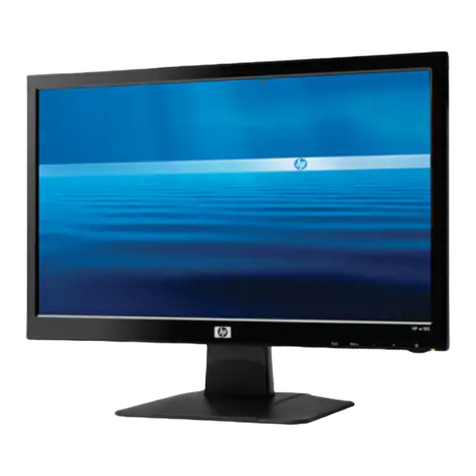
HP WF1907 - Compaq 19" LCD Monitor User manual

Published by LITE-ON Service Printed in Taiwan All rights reserved Subject to modification 31th Oct-2006©
Any person attempting to service this chassis must familarize with the chassis and be aware of the necessary safety
precautions to be used when serving electronic equipment containing high voltage.
June.19th-2006
Service Manual
Service
HP
HP 1907 & W1907WF
HP_LCD_W1907&WF1907_SM061031V00
Table of Contents
01. ----------------------------------------------------------------01
02. --------------------------------------------------------------------------------------02
03. --------------------------------------------------------------------------------03
04. ------------------------------------------------------------------------------------10
05. -------------------------------------------------------------------------------------------24
Power Board Operation Theory
Inverter Circuit
Interface Operation
Troubleshooting
Schematic
Safety Notice
022-83718162
www.chinadse.org
022-83715667

Page 1
HP W1907& WF1907 Service Manual
1. Power Board Operation Theory
1.1
Line
filter
consists
of
C801,
T801,
C802,
C803,
C804,
C808,
C809,
C815,
C819,
C820,
C825.
It
eliminates
high
frequency interference
to
meet
EMI’s
requirement.
1.2
Rec
&
Filter
Bridge
diode
D812,
D813,
D814,
D815
converts
AC
source
into
pulsed
DC.
This
pulsed
DC
is
smoothed
and filtered
by
C805.
R802
is
an
NTC
(negative
thermal
coefficient
)
resistor,
used
to
reduce
inrush
current
to
be within
safe
range.
1.3
Power
transformer
:
T802
converts
energy
for
square
wave
from
power
source
C805
to
secondary
side
to
generate
+5V,
+12V
and +22V.
1.4
Output
:
The
square
wave
from
T802
is
rectified
by
D808
D809,
D810,
then
filtered
by
C817,
C818,
C824,
C823,
C830,
C833, C822
to
generate
+22.5V
and
+12V,
+5V
respectively.
1.5
Driver
:
Q803
drive
T802
from
PWM
control
of
I801
for
power
converted.
1.6
FB
:
Negative
feedback
CKT
consists
of
photo
coupler
I802
and
adjustable
regulator
I803.
It
can
maintain
output voltages
+22.5V
and
+12V,
+5V
at
a
stable
level.
1.7
PWM
:
1.7.1
Start
:
When
power
is
turned
on.
C807
is
charged
a
11V
and
a
starting
current
above
40uA
to
pin
1
of
I801. I801
starts
to
oscillate
and
outputs
a
pulse
train
through
pin
6
to
drive
Q803.
1.7.2
OPP
:
When
Q803
turns
on,
C805
supplies
a
linearly
increasing
triangle
current
through
the
primary
inductance
of
T802
to
the
driver
Q803,
once
the
peak
value
of
this
current
multiplied
by
R811
exceeds
0.52V,
pulse train
will
be
turn
off
immediately
to
protect
Q803,
T802
from
being
burned
out.
1.7.3
Regulation
:
If
output
voltage
+22V
goes
up,
the
R
terminal
of
I803
gets
more
bias,
accordingly
photo transistor
and
photo
diode
flows
more
current.
The
voltage
of
pin
2
goes
up
too,
making
the
pulse
width
of pin
6
to
become
narrower.
So
the
output
voltage
+22V
will
be
pulled
down
to
a
stable
value.
1.7.4
OVP
:
If
+22.5V
goes
up
too
much,
the
induced
voltage
on
pin
4
of
T802
becomes
large
also.
Suppose
that
it is
over
20V.
The
pulse
train
at
pin
6
goes
down
to
zero,
shutting
Q803
off
immediately.
1.7.5 SCP
:
If
output
terminal
is
short
to
ground,
photo
transistor
does
not
conduct,
hence
I802
does
not
conduct either.
Then
oscillation
of
I801
is
stop,
shutting
Q803
off
immediately.
022-83718162
www.chinadse.org
022-83715667

Page 2
2. Inverter Circuit
This
unit
operates
on
an
output
voltage
of
22V
from
power
source.
2.1 VDD:
R105
get
a
+5VDC
for
I101
power
supply.
2.2 Control
IC:
I101
(OZ9938)
2.2.1 Enable
:
When
pin
1
of
I101
is
over
2V,
I101
works.
If
it
is
under
1V,
I101
turns
off.
2.2.2
OSC:
When
I101
enabled,
C104/R118/R107
(pin
13
of
I101)
determine
the
operating
frequency.
2.2.3
SST:
C106
(pin
12
of
I101)
provides
soft
start
function.
2.2.4
Ignition:
IC
provides
higher
operating
frequency
internally
for
more
striking
voltage
until
regulation
of
feedback
of lamp
current.
And
provide
2
sec
striking
time.
2.2.5
Dimming
control:
The
external
PWM
voltage
of
R136/C111
control
the
duty
pulse
of
burst-mode
to
drive
and perform
a
wide
dimming
control
for
the
CCFL.
The
burst-mode
frequency
is
determined
by
scalor
IC.
2.2.6
Regulation:
Pin
5
of
I101
provide
regulation
of
the
CCFL
current
from
feedback.
The
non-inverting
reference
is
at 1.25V
nominal.
2.2.7
Protection:
Open-lamp
protection
in
the
ignition
period
is
provided
through
pin
6
of
I101.
Removal
of
the
CCFL
during
normal
operation
will
trigger
IC
to
turns
on
and
shuts
off
the
inverter.
This
is
latch function.
2.2.8 Output
drivers:
The
configuration
prevents
any
shoot-through
issue
associated with
bridge-type
power conversion
applications.
Adjusting
the
overlap
conduction
between
Q104,
Q105,
the
CCFL
current
regulation
is achieved.
2.3
Half-bridge
switching/Transformer:
Q104,
Q105,
C122,
C123,
C134
compose
half-bridge
switching
to
convert
DC into
AC
for
driver
the
CCFL.
2.4 Detection:
C112,
C114,
C115,
C116,
C118,
C119,
R126,
R116,
R115,
R117,
R119,
R121,
R122,
R125
detect
the
output voltage
and
ensure
a
rated
voltage
by
pin
6
of
I101
ensure
not
a
open-lamp.
2.5 Feedback:
D116,
D117,
D120,
D121,
R111,
R130
sense
the
lamp
current
for
negative
feedback
and
regulation.
022-83718162
www.chinadse.org
022-83715667

Page 3
3. Interface Operation
3.1 Top (Circuit diagrams sheet 2 of 8)
This page is function block. (1) Power. (2) VGA & DDC interface. (3) DVI & DDC interface. (4)
Scaler Gm5726H (Gm5766H). (5) Key & panel interface. (6) Audio.
3.2 Power (Circuit diagrams sheet 3 of 8)
3.2.1 P301 connector
A 5V power supply for LCD module, also it is main power of interface board. A VDD (+5V)
power supply for audio AMP. It is generated from the P301 connector. And adjust back
light of LCD module from I306 sclaer Gm5726H (Gm5766H) control.
3.2.2 I302 : 3-terminal regulator
A 3.3V power supply for I306 scaler IC Gm5726H (Gm5766H) and I308 EEPROM / I309
SPI flash ROM, it is generated from the 5V source.
3.2.3 I303 : 3-terminal regulator
A 1.8V power supply for I306 scaler IC Gm5726H (Gm5766H), it is generated from the
3.3V source (I302).
3.2.4 Q302, I301 : ON/OFF control for LCD module power
ON/OFF control (PANELVCC_EN) is performed for power ON/OFF and also for the power
saving sequence. It is support 5V to LCD module power. The PANELVCC_EN signal is
generated from I306 scaler IC Gm5726H (Gm5766H).
3.2.5 R305 : ON/OFF control for LCD module back light power
ON/OFF control (BKLT_EN) is performed for black light power ON/OFF and also for the
power saving sequence. The BKLT_EN signal is generated from I306 scaler IC
Gm5726H (Gm5766H).
022-83718162
www.chinadse.org
022-83715667

Page 4
3.2.6 Q301, R301, R302, R304 : Adjust back light luminance of LCD module
It is adjusted back light luminance control (BKLT_ADJ) is performed for the back light
luminance. The BKLT_ADJ signal is generated from I306 scaler IC Gm5726H (Gm5766H).
3.3 VGA & DDC interface (Circuit diagrams sheet 4 of 8)
This sheet has RGB analog video and H/V sync signals input from VGA connector.
The RGB analog video signals input through AC-coupled, analog video signal is used to clamp the
black level at 0V. And H/V sync to sclaer.
Support EDID plug & play function for analog video.
It is to support VESA DDC/CI interface for analog video.
3.3.1 P302 connector
The RGB analog video and H/V sync input signals to I306 scaler Gm5726H (Gm5766H).
The VESA DDC/CI function is through I2C bus to I306 scaler Gm5726H (Gm5766H).
3.3.2 I304 : EDID EEPROM (24LC02B)
The I304 is support EDID information of the VESA standard for VGA interface, and support
plug and play for the PC host.
3.4 DVI & DDC interface (Circuit diagrams sheet 5 of 8)
The digital video signals (TMDS) input from P303 DVI-D connector. The digital video signal is
TMDS for DVI V1.0 standard. And support EDID plug & play function for digital video.
It is to support VESA DDC/CI interface, and support HDCP function.
3.4.1 P303 connector
P303 is DVI-D connector for DDWG standard, it have digital video signals (TMDS) to I306
scaler Gm5726H (Gm5766H). The VESA DDC/CI function is through I2C bus to I306
Gm5726H (Gm5766H). And support HDCP function is also through I2C bus to I306
Gm5726H (Gm5766H).
3.4.2 I305 : EDID EEPROM (24LC02B)
The I305 is support EDID information of the VESA standard for DVI interface, and support
plug and play for the PC host.
3.5 Scaler Gm5726H (Gm5766H) (Circuit diagrams sheet 6 of 8)
The I306 Gm5726H (Gm5766H) is all-in-one LCD monitor controller. The Gm5726H (Gm5766H)
leverages Genesis patented advanced image-processing technology as well as a proven
integrated ADC/PLL and an Ultra-Reliable DVI compliant receiver to provide excellent image
quality. Gm5726H (Gm5766H) also integrates HDCP function, a micro-controller, an OSD
controller, and dual LVDS.
The RGB analog video signal from video input circuit enter to incorporated A/D converted block
(ADC) into the digital data for analog video signal.
The TMDS digital signals input (with HDCP) entered from the DVI-D connector is converted into
the digital data.
Based on this conversion, this device performs interpolation during pixel extension. These
interpolation digital data are transformed to LVDS signal. The I306 source voltage is 3.3V and
1.8V, the device clock source frequency is 14.318 MHz. And support DDC/CI interface of VESA
and function key operation.
022-83718162
www.chinadse.org
022-83715667

Page 5
3.5.1 I308 EEPROM (24LC16B)
The control data and parameter, and OSD related setting, and other service data, to be
stored in I308. The contents of which are updated as required.
3.5.2 I309 SPI Flash ROM
The firmware program running from I309 external SPI flash ROM, contains firmware code
and data for all firmware function. The device is 2Mbits of flash ROM.
3.5.3 I307 Microprocessor Supervisory Circuit
The function of this device is to assert a reset to I306 scaler Gm5726H (Gm5766H), when
either the power supply dropped down.
3.5.4 X301 14.318MHz
It generated reference clock input for I306 scaler.
3.5.5 ISP and DDC/CI function
The DDC/CI is VESA standard for the host PC system, it can through I2C bus to control
LCD monitor. Enter I306 pin64 DDC_SCL_A and pin65 DDC_SDA_A of the VGA port.
Enter I306 pin66 DDC_SCL_D pin67 DDC_SDA_D of the DVI-D port.
It use ISP function when change new firmware to I309 SPI flash ROM, it used I2C bus
from VGA or DVI-D port through I306 Gm5726H (Gm5766H) to I309 SPI flash ROM.
3.5.6 The power save sequence function
First I306 pin49 (BKLT_EN) set Low to disable LCD module back light power, delay of
some time, then I306 pin127 (PANELVCC_EN) set Low to disable LCD module power,
then I306 enter to power down mode.
3.6 Key & Panel interface (Circuit diagrams sheet 7of 8)
3.6.1 P306 connector
It is LVDS bus, it is from I306 scaler to LCD panel module. The P306 output voltage is 5V.
3.6.2 P307 and P308 connector
The P307/P308 has support keypad function. Control is give effect to for the push switch to
be used when the user changes the parameters, in order to modify the respective setting
values. Whether the switch has been pressed is identified with the switch input level
change of I306 Gm5726H (Gm5766H). Related ports of I306 based on Table 1.
Each parameter is stored in the I308 EEPROM, the contents of which are updated as
required. The P307 have LED Blue and Amber light, the LED Blue signal from I306
pin126, and the LED Amber signal from I306 pin125.
Table 1 Related ports of I306
Pin No. I/O Signal name Function Remarks
Pin 113 I KEY_POWER Soft power switch input Power key
Pin 115 I KEY_MENU Enter OSD switch input Enter OSD menu
Pin 114 I KEY_UP Switch input Up key or Viewing model selection
Pin 115 I KEY_DOWN Switch input Down key or Volume control of
audio function
Pin 114 I KEY_SELECT Selection switch input Select key or Auto adjust key
3.7 Audio (Circuit diagrams sheet 8of 8)
3.7.1 P309 connector
022-83718162
www.chinadse.org
022-83715667

Page 6
The P309 is audio signal input from the audio source.
3.7.2 P310 connector
The P310 is audio output to speaker and support 2W x 2 speakers.
3.7.3 I310 TPA6021A4
The I310 is 2x2W stereo audio amplifier, it is an integrated class-AB dual output amplifier.
3.7.4 Q309 : Power down and mute control for Audio
ON/OFF control (AUDIO_EN) is performed for standby mode and mute function. It is
support 5V to audio IC power. The AUDIO_EN signal is generated from I306 scaler
Gm5726H (Gm5766H).
3.7.5 R394, Q310: Volume control for Audio
Volume control (volume) is performed for audio output signal power. The volume signal is
generated from I306 scaler Gm5726H (Gm5766H).
3.8 Others
3.8.1 Detection of POWER ON status
The I306 Gm5726H (Gm5766H) identified the ON status of two modes for the power
supplies. The identification is made when the power supply is turn off. For example, if the
power supply is turn off with the POWER key switch, the POWER key switch must be turn
on when active the power supply again. If the power supply turned off by the pulling out the
power cord, then this power supply can to be turned on by connecting the power cord,
without pressing the POWER key switch.
3.8.2 Display mode identification
3.8.2.1 Display mode identification
zThe display mode of input signal is identified based on Table 2.
zWhen the mode has been identified through the measurement of horizontal
and vertical frequencies, the total number of lines is determined with a formula of
“Horizontal frequency / Vertical frequency = Total number of number of lines”.
Final identification can be made by examining the coincidence of the obtained
figure with the number of lines for the mode identified from the frequency. The
Distinction Hsync and Vsync of each mode is shown in Table 3.
zWhen the detected frequency if the sync signal has changed, the total number
of lines should be counted even through it is range identified frequency in the
same mode.
3.8.2.2 Out of range
This out of range mode is assumed when the frequency out of the horizontal /
vertical signal is as specified below.
zVertical frequency : 50 ~ 76 Hz.
zHorizontal frequency : 24 ~ 83KHz.
3.8.2.3 Power save mode
The power save mode is assumed when the horizontal / vertical signals are as
specified below.
zIf there is no horizontal sync signal input.
zIf there is no vertical sync signal input.
zIf the horizontal sync signal is outside the measuring range of I306 Gm5726H
(Gm5766H).
zIf the vertical sync signal is outside the measuring range of I306 Gm5726H
022-83718162
www.chinadse.org
022-83715667
Page 7
(Gm5766H).
Table 2 video mode
Polarity
Mode Resolution H-Freq (KHz) Band Width (MHz) H V
1 640x480 (59.94Hz) 31.469 25.175 - -
2 640x480 (72Hz) 37.861 31.5 - -
3 640x480 (75Hz) 37.5 31.5 - -
4 720x400 (70Hz) 31.469 28.322 - +
5 800x600 (60Hz) 37.879 40 + +
6 800x600 (72Hz) 48.077 50 + +
7 800x600 (75Hz) 46.875 49.5 + +
8 832x624 (74.55Hz) 49.722 57.284 +/- +/-
9 1024x768 (60Hz) 48.363 65 - -
10 1024x768 (70Hz) 56.476 75 - -
11 1024x768 (75Hz) 60.023 78.75 + +
12 1152x870 (75Hz) 68.68 100 - -
13 1152x900 (76Hz) 71.71 105.561 - -
14 1280x1024 (60Hz) 63.981 108 + +
15 1280x1024 (75Hz) 79.976 135 + +
Table 3 the Hsync, Vsync distinction
Indication resolution Distinction Hsync Distinction Vsync The fixed mode
720 x 400 30.5KHz≦fH≦32.5KHz 69Hz≦fV≦71Hz 4
640 x 480 30.5KHz≦fH≦32.5KHz 59Hz≦fV≦61Hz 1
640 x 480 36.9KHz≦fH≦38.9KHz 71.8Hz≦fV≦73.8Hz 2
640 x 480 36.5KHz≦fH≦38.5KHz 74Hz≦fV≦76Hz 3
800 x 600 36.9KHz≦fH≦38.9KHz 59.3Hz≦fV≦61.3Hz 5
800 x 600 47.1KHz≦fH≦49.1KHz 71.2Hz≦fV≦73.2Hz 6
800 x 600 45.9KHz≦fH≦47.9KHz 74Hz≦fV≦76Hz 7
832 x 624 48.7KHz≦fH≦50.7KHz 73.5Hz≦fV≦75.5Hz 8
1024 x 768 47.4KHz≦fH≦49.4KHz 59Hz≦fV≦61Hz 9
1024 x 768 55.5KHz≦fH≦57.5KHz 69.1Hz≦fV≦70.1Hz 10
1024 x 768 59KHz≦fH≦61KHz 74Hz≦fV 76Hz≦11
1152 x 870 67.7KHz fH 69.7KHz≦≦ 74Hz fV 76Hz≦≦ 12
1152 x 900 70.7KHz fH 72.7KHz≦≦ 75Hz fV 77Hz≦≦ 13
1280 x 1024 62.9KHz fH 64.9KHz≦≦ 59Hz fV 61Hz≦≦ 14
1280 x 1024 79KHz fH 81KHz≦≦ 74Hz fV 76Hz≦≦ 15
3.8.3 Power ON sequence
When the POWER key switch is pressed, the POWER key switch signal is turned “H”.
When this “H” potential is detected, the CPU begins to establish the respective power
022-83718162
www.chinadse.org
022-83715667
Page 8
supplies according to the sequence show below.
3.8.4 Power OFF sequence
When the POWER key switch is pressed, while the power supply is ON, the POWER key
switch signal is turned “H”. When this “H” potential is detected, the CPU begins to turn off
the respective power supplies according to sequence show below.
460ms
157ms
140ms
140ms
Power Key
LED Blue
PANELVCC_E
N
BKLT_EN
AUDIO_EN
296ms
Power Key
LED Blue
PANELVCC_E
N
BKLT_EN
AUDIO_EN
516ms
825ms
3.68s
022-83718162
www.chinadse.org
022-83715667
Page 9
3.8.5 List of I/O Pin Assignments of the I306
Pin No. Port Signal Name Initial Setting Function
113 LBADC_IN3 PWR_KEYn H ON/OFF LCD monitor
126 GPIO14 LED_B L LED Blue enable when is H
125 GPIO13 LED_A L LED amber enable when is H
114 LBADC_IN2 KEY_UPn H OSD up/plus enable when is 2.46V
115 LBADC_IN1 KEY_MENUn H OSD enter enable when is 2.46V
114 LBADC_IN2 KEY_SELECTn H OSD select/exit enable when is 2.0V
115 LBADC_IN1 KEY_DOWNn H OSD down/minus enable when is 2.0V
86 GPIO31 HDCP_HPDn L DVI HPD enable when is L
122 GPIO10 SCL H EEPROM clock signal of IIC bus
123 GPIO11 SDA H EEPROM data signal of IIC bus
50 GPO4 BKLT_ADJ - Backlight brightness control
124 GPIO12 DDC_WPn L DDC EEPROM write protection when is
L
51 GPO0 AUDIO_EN L Audio enable when is H
56 GPO1 VOLUME L Audio volume
121 GPIO9 VGA_DETn H VGA cable connected when is L
120 GPIO8 DVI_DETn H DVI cable connected when is L
58 GPO3 UART_DO H UART interface data OUT
57 GPO2 UART_DI H UART interface data IN
127 PPWR PANELVCC_EN L Panel power enable when is H
49 PBIAS BKLT_EN L Back light power enable when is H
64 GPIO16 DDC_SCL_VGA H DDC/CI interface for VGA
65 GPIO17 DDC_SDA_VGA H DDC/CI interface for VGA
66 GPIO18 DDC_SCL_DVI H DDC/CI interface for DVI
67 GPIO19 DDC_SDA_DVI H DDC/CI interface for DVI
022-83718162
www.chinadse.org
022-83715667

4. Troubleshooting
Does OSD display when you push MENU
button.
Ye s
No Proceed "No OSD display" section.
Checkifthesyncsignalfromcomputeris
output and if the video cable is connected
normally. (VGA or DVI)
OK
Proceed "checking the resolution change IC
movement" section.
NG Input the sync signal of computer, or change
the cable. (VGA or DVI)
When a signal isn't being input, it is
indicated with "VIDEO INPUT". it is
indicated with "OUT OF RANGE" at the
time of the frequency that it can't be
distinguished.
Page 10
4.1 No.display of screen (Screen is black, color of LED is amber)
022-83718162
www.chinadse.org
022-83715667
4.2 Nothing display on screen screen is black, color of LED is blue(
Is backlight light up?
Refer "Checking the backlight unit" section”
OK
NG
Does computer output RGB video signals?
(VGA or DVI)
OK
Check OSD menu is display on screen when
you push the "MENU" key.
Proceed "Abnormal sreen" dection"
OK
NG
Check the video cable for failure. Check the host for output signal with all
black only.
1) Change pattern of video signal output on the host.
2) Reconnect the video cable.
3) Change the video cable. (VGA or DVI)
NG Check if the LCD module signal cable is connected between the I nterface
Board and LCD module.
OK
Next Page
NG
Failure Point
The LVDS cable is disconnected.
Page 11
022-83718162
www.chinadse.org
022-83715667
Continue
Check the 3.3V power are supplied on I302 pin 2, 4.
OK
NG Check if the voltage on I302 pin 3 that is
power DC at 5V.
OK
Failure Point
I302 is failure.
NG
Failure Point
1) Printed wire broke between P301 pin 5, 6
and I302.
2) FB301, FB302 are open.
3) Check power board.
Check the 1.8V power are supplied on I303 pin 2, 4.
Check if the voltage on I303 pin 3 that is
power DC at 3.3V from the I302.
OK
Failure Point
I303 is failure.
NG
Failure Point
1) Printed wire broke between I302 pin 2, 4
and I303 pin 3.
2) I302 is failure.
OK
NG
Next Page
Page 12
022-83718162
www.chinadse.org
022-83715667
Check the 5V power are supplied on P306
pin1,2,3(totheLCDpanel)
Continue
OK
NG Check if the Voltage on I301 pin 2 that is
DC power at 5V.
OK
NG
Failure Point
1) Printed wire broke between P301 pin 5,
6, and I301 pin 2.
2) FB301 or FB302 or FB303 is open.
Check if the MOS FET Gate level on I301
pin 1, that Gate level is low.
OK
NG
OK
NG
Failure Point
1) Printed wire broke between Q302
pin 3, R307, R308, C309 and I301 pin
1.
2) Q302 is failure.
Failure Point
1) Printed wire broke between Q302 pin 2
and I306 pin 127.
2) I306 is failure.
Check the PANELVCC_EN signal of the
Q302 pin 2 (with R309) at high level.
Failure Point
I301 is failure.
Check the P306 all LVDS signals.
Failure Point
1) Printed wire broke between P306 and
I306 LVDS signals.
2) I306 is failure.
Failure Point
1) The LVDS cable broke between P306
and LCD module.
2) LCD module is failure.
OK
NG
Page 13
022-83718162
www.chinadse.org
022-83715667

Is +20V supplied to inverter PWB ? (by the
power board)
4.3 Checking the back light unit
OK
NG
Failure Point
1) Inverter cable disconnection.
2) Power board failure.
Check the BACKLIGHT_EN signal of the
P301 pin 2 at high level.
OK
NG
Failure Point
1) printed wire broke between P301 pin 2,
R305 and I306 pin 49.
2) R305 is open, or R306, C308 are short.
3) I306 is failure.
Check the BACKLIGHT_ADJ signal of the
P302 pin 3 from I306 pin 50 is a PWM
signal.
OK
NG
Failure Point
1) printed wire broke between P301 pin 3,
Q301 and I306 pin 50.
2) Q301 is failure.
3) R301 or R302 or R304 is open, or C304
is short.
4) I306 is failure.
Failure Point
Back light unit of LCD module is failure.
Page 14
022-83718162
www.chinadse.org
022-83715667
4.4 Abnormal screen
Check the R, G, B video signal from computer
input on P302 of video connector.
OK
NG Failure Point
1) No R, G, B video signals output from host
computer, check computer.
2) VGA video signal cable disconnection.
ChecktheR,G,BinputvideosignalsonI306pin
99, 96, 93 respectively that their level is 0.5 to
1.0Vp-p.
Failure Point
In the case of the Red signal. (Green and Blue
signal is the same path, too.)
1) Printed wire broke between P302 pin 1 and
I306 pin 99.
2) Video cable is failure.
3) FB3305, FB306, R313 are open.
4) R313 are short.
5) C317 is short or open.
NG
OK
Check all LVDS signals being output to P306
from I306?
Failure Point
1) Printed wire broke between I306 and P306.
2) LVDS wire failure.
NG
OK
Prpcess "Checking the resolution change IC
movement" section.
4.4.1 Abnormal screen for VGA source
Page 15
Check the H, V SYNC input signals on I306 pin
89, 90 respectively that signal and level.
NG
OK
Failure Point
1) Printed wire broke between I306 and P302.
2) FB311, FB312, R321, R322 are open.
3) R323, R324 if is 2.4K ohm.
4) D305, D306, C327, C328 are short.
5) Video cable is failure.
022-83718162
www.chinadse.org
022-83715667

Check the TMDS signal from computer input on
P303 of DVI-D video connector.
OK
NG Failure Point
1) No TMDS signals output from host computer,
check computer.
2) DVI-D video signal cable disconnection.
Check the TMDS input video signals on I306 pin
72, 73, 75, 76, 80, 81, 83, 84 respectively that
their differential input voltage is 150 to 1200 mV.
Failure Point
In the case of the RX2+/- signal. (A RX1, 0, and
RXC signal is the same path, too.)
1) Printed wire broke between P303 pin 1, 2 and
I306 pin 72, 73.
2) DVI-D video cable is failure.
3) R332, R333 is open.
NG
OK
Check all LVDS signals being output to P306
from I306?
Failure Point
1) Printed wire broke between I306 and P306.
2) LVDS cable failure.
NGOK
Prpcess "Checking the resolution change IC
movement" section.
4.4.2 Abnormal screen for DVI source
Page 16
Check the HP output signal to P303 pin 16
respectively that voltage is 4.0 to 5 V.
NG
OK
Failure Point
The HP is high will to generated TMDS from PC
host.
1) Check P303 pin 14 if is 5V.
2) Printed wire broke between P303 pin 14 and
Q305.
3) C343, C344 is short.
4) Q305 is failure.
5) DVI-D cable is failure.
6) Printed wire broke between Q305 and I306 pin
86.
7) R361 is open. Q305 is failure.
8) I306 is failure.
022-83718162
www.chinadse.org
022-83715667
4.5 Abnormal OSD display adjust problem
Check the input level whether was changed when pressed
function keys on the P308 pin 2, 3, 4, 5. (normal is 3.3V,
when push button, generated different voltage. pin 2, 4 is
2.46V, pin 3, 5 is 2V)
OK
NG Failure Point
1) Function key wire disconnection.
2) Function key wire is failure.
3) Function key board is failure.
Check the input voltage level whether was changed when
pressed function keys on the I306 pin 114, 115. (normal is
3.3V, when push button, generated 2.46V or 2V.)
OK
NG
Failure Point
1) Printed wire broke between P308 pin 2 and I306 pin 115.
2) Printed wire broke between P308 pin 3 and I306 pin 115.
3) Printed wire broke between P308 pin 4 and I306 pin 114.
4) Printed wire broke between P306 pin 5 and I306 pin 114.
5) C381, C382, R367, R368, C387, C388, C389, C390, C391, C392
is short.
6) R378, R379, R381, R382, R384, R385 is short or open.
7) R380, R383 is open.
Failure Point
I306 is failure.
Page 17
022-83718162
www.chinadse.org
022-83715667
4.6 Abnormal plug and play operation
Confirm the host computer supplies DDC/CI mode.
OK
NG Failure Point
The host machine is not communicated in DDC/CI
mode.
Check the voltage on I304 pin 8 that is DC 5 V.
OK
NG Failure Point
1) Printed wire broke between I304 pinv8, D307 and
P302 pin 9.
2) D307 is failure.
Check the output signal of I2C data / clk on I304 pin 5,
6.
OK
NG Failure Point
I304 is failure.
Check the voltage on P302 pin 9 that is DC 5 V.
OK
NG Failure Point
TheVGAvideocableisfailure.
Check the signals if is high level on P302 pin 12, 15
that is I2C data / clk signal.
OK
NG Failure Point
TheVGAvideocableisfailure.
Failure Point
1) Printed wire broke between I306 pin 65, 64, I304 pin
5, 6 and P302 pin 12, 15.
2) I306 maybe failure.
3) R328, R329 is open.
4) C331, C332, R326, R327 is short.
4.6.1 Abnormal plug and play operation for VGA
Page 18
022-83718162
www.chinadse.org
022-83715667

Confirm the host computer supplies DDC/CI mode.
OK
NG Failure Point
The host machine is not communicated in DDC/CI
mode.
Check the voltage on I305 pin 8 that is DC 5 V.
OK
NG Failure Point
1) Printed wire broke between I305 pin 8, D320 and
P303 pin 14.
2) D320 is failure.
Check the output signal of I2C data / clk on I305 pin 5,
6.
OK
NG Failure Point
I305 is failure.
Check the voltage on P303 pin 14 that is DC 5 V.
OK
NG Failure Point
The DVI-D video cable is failure.
Check the signals if is high on P301 pin 7, 6 that is I2C
data / clk signal.
OK
NG Failure Point
The DVI-D video cable is failure.
Failure Point
1) Printed wire broke between I306 pin 67, 66, I305 pin
5,6andP303pin7,6.
2) I306 maybe failure.
3) R346, R347 is open.
4) C346, C347, R324, R343 is short.
4.6.2 Abnormal plug and play operation for DVI
Page 19
022-83718162
www.chinadse.org
022-83715667
Other manuals for WF1907 - Compaq 19" LCD Monitor
2
This manual suits for next models
1
Table of contents
Other HP Monitor manuals

HP
HP EliteDisplay E232e Installation instructions

HP
HP XP598AA#ABA User manual

HP
HP WF1907 - Compaq 19" LCD Monitor How to use

HP
HP EliteDisplay E240e Installation instructions

HP
HP L1940T User manual

HP
HP L1910i User manual

HP
HP L200hx Installation instructions

HP
HP Pavilion f1503 Specification sheet

HP
HP ElitePOS 10 Installation instructions

HP
HP V273a Installation instructions