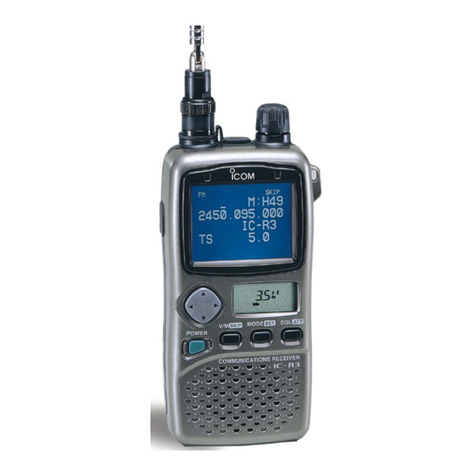
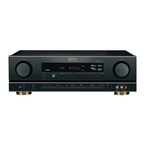
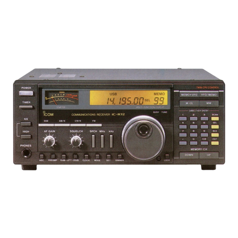
Icom IC-R9500 User manual

S-14323XZ-C1-q
Oct. 2007
COMMUNICATIONS RECEIVER

This service manual describes the latest service information
for the IC-R9500 COMMUNICATIONS RECEIVER at the
time of publication.
NEVER connect the transceiver to an AC outlet or to a DC
power supply that uses more than specified. This will ruin
the transceiver.
DO NOT apply an RF signal of more than 20 dBm (100 mW)
to the antenna connector. This could damage the receiver’s
front end.
To upgrade quality any electrical or mechanical parts and
internal circuits are subject to change without notice or
obligation.
MODEL VERSION FREQUENCY COVERAGE (MHz)
IC-R9500
[USA]
0.005–821.999999,
851.000000–866.999999,
896.000000–3335.000000
[FRA]
0.0050000–29.999999,
50.200000–51.200000,
87.500000–108.000000,
144.000000–146.000000,
430.000000–440.000000,
1240.000000–1300.000000
[USA-01]
0.005–3335.000000
[EUR]
[UK]
[CAN]
[EXP]
[AUS]
[CHN]
Be sure to include the following four points when ordering
replacement parts:
1. 10-digit order numbers
2. Component part number and name
3. Equipment model name and UNIT name
4. Quantity required
<SAMPLE ORDER>
1110006750 S.IC TK14570L IC-R9500 RF-A UNIT 5 pieces
8820001210 Screw 2844 screw IC-R9500 CHASSIS 10 pieces
Addresses are provided on the inside back cover for your
convenience.
Icom Icom Inc. and logo are registered trademarks of Icom Incorporated (Japan) in the United States the United
Kingdom Germany France Spain Russia and/or other countries.
ORDERING PARTS
1. Make sure a problem is internal before disassembling
the receiver.
2. DO NOT open the receiver until the receiver is
disconnected from its power source.
3. DO NOT force any of the variable components. Turn
them slowly and smoothly.
4. DO NOT short any circuits or electronic parts. An
insulated tuning tool MUST be used for all adjustments.
5. DO NOT keep power ON for a long time when the
receiver is defective.
6. READ the instructions of test equipment throughly
before connecting equipment to the receiver.
REPAIR NOTES
INTRODUCTION CAUTION

CONTENTS
SECTION 1 SPECIFICATIONS
SECTION 2 INSIDE VIEWS
SECTION 3 CIRCUIT DESCRIPITON
3-1 RECEIVER CIRCUITS. . . . . . . . . . . . . . . . . . . . . . . . . . . . . . . . . . . . . . . . . . . . . . . . . . . . . . . . 3-1
3-2 FREQUENCY SYNTHESIZER CIRCUITS . . . . . . . . . . . . . . . . . . . . . . . . . . . . . . . . . . . . . . . . 3-1
3-3 LOGIC CIRCUITS . . . . . . . . . . . . . . . . . . . . . . . . . . . . . . . . . . . . . . . . . . . . . . . . . . . . . . . . . . . 3-5
3-4 POWER SUPPLY CIRCUITS. . . . . . . . . . . . . . . . . . . . . . . . . . . . . . . . . . . . . . . . . . . . . . . . . . . 3-1
3-5 PORT ALLOCATIONS . . . . . . . . . . . . . . . . . . . . . . . . . . . . . . . . . . . . . . . . . . . . . . . . . . . . . . . . 3-5
SECTION 4 ADJUSTMENT PROCEDURES
4-1 PREPARATION . . . . . . . . . . . . . . . . . . . . . . . . . . . . . . . . . . . . . . . . . . . . . . . . . . . . . . . . . . . . . 4-1
4-2 EXT. S-METER AND REFERENCE FREQUENCY ADJUSTMENTS . . . . . . . . . . . . . . . . . . . . 4-3
4-3 VCO ADJUSTMENTS . . . . . . . . . . . . . . . . . . . . . . . . . . . . . . . . . . . . . . . . . . . . . . . . . . . . . . . . 4-3
4-4 RECEIVE ADJUSTMENT (HF) . . . . . . . . . . . . . . . . . . . . . . . . . . . . . . . . . . . . . . . . . . . . . . . . . 4-4
4-5 RECEIVE ADJUSTMENT (V/U) . . . . . . . . . . . . . . . . . . . . . . . . . . . . . . . . . . . . . . . . . . . . . . . . 4-6
4-6 RECEIVE ADJUSTMENT (V/U1) . . . . . . . . . . . . . . . . . . . . . . . . . . . . . . . . . . . . . . . . . . . . . . . 4-7
4-7 RECEIVE ADJUSTMENT (V/U2) . . . . . . . . . . . . . . . . . . . . . . . . . . . . . . . . . . . . . . . . . . . . . . . 4-14
4-8 RECEIVE ADJUSTMENT (TV) . . . . . . . . . . . . . . . . . . . . . . . . . . . . . . . . . . . . . . . . . . . . . . . . . 4-21
4-9 RECEIVE ADJUSTMENT (WFM) . . . . . . . . . . . . . . . . . . . . . . . . . . . . . . . . . . . . . . . . . . . . . . . 4-22
SECTION 5 PARTS LIST
SECTION 6 MECHANICAL PARTS AND DISASSEMBLY
SECTION 7 BOARD LAYOUTS
LOGIC UNIT . . . . . . . . . . . . . . . . . . . . . . . . . . . . . . . . . . . . . . . . . . . . . . . . . . . . . . . . . . . . . . . 7-1
MAMORY BOARD . . . . . . . . . . . . . . . . . . . . . . . . . . . . . . . . . . . . . . . . . . . . . . . . . . . . . . . . . . . 7-1
ANT, BPF, MIX1, MIX2 UNITS. . . . . . . . . . . . . . . . . . . . . . . . . . . . . . . . . . . . . . . . . . . . . . . . . . 7-3
RF-A, RF-B UNITS . . . . . . . . . . . . . . . . . . . . . . . . . . . . . . . . . . . . . . . . . . . . . . . . . . . . . . . . . . 7-5
VCO-A~C, VCO2, FIL1/2 BOARDS AND PLL UNIT . . . . . . . . . . . . . . . . . . . . . . . . . . . . . . . . . 7-7
SW-A~C, VR-A~F, SENSOR, TENKEY, LED, DISPLAY BOARDS . . . . . . . . . . . . . . . . . . . . . . 7-9
JACK BOARD AND CONNECT-A/B OSC UNITS . . . . . . . . . . . . . . . . . . . . . . . . . . . . . . . . . . 7-11
MAIN, SCOPE/TV, DC-DC UNITS. . . . . . . . . . . . . . . . . . . . . . . . . . . . . . . . . . . . . . . . . . . . . . . 7-13
i

ii
CONTENTS (continued)
SECTION 8 WIRING DIAGRAM
SECTION 9 BLOCK DIAGRAM
SECTION 10 SCHEMATIC DIAGRAM
LOGIC UNIT AND MAMORY BOARD. . . . . . . . . . . . . . . . . . . . . . . . . . . . . . . . . . . . . . . . . . . . 10-1
MAIN UNIT. . . . . . . . . . . . . . . . . . . . . . . . . . . . . . . . . . . . . . . . . . . . . . . . . . . . . . . . . . . . . . . . . 10-6
VCO-A~C, VCO2, FIL1/2 BOARDS AND PLL UNIT . . . . . . . . . . . . . . . . . . . . . . . . . . . . . . . . . 10-10
ANT, BPF, RF-A, RF-B, MIX1, MIX2 UNITS . . . . . . . . . . . . . . . . . . . . . . . . . . . . . . . . . . . . . . . 10-15
SW-A~C, VR-A~F, SENSOR, TENKEY, LED, DISPLAY,
JACK BOARD AND CONNECT-A/B UNITS . . . . . . . . . . . . . . . . . . . . . . . . . . . . . . . . . . . . . . . 10-21
OSC, SCOPE/TV, DC-DC, REG UNITS . . . . . . . . . . . . . . . . . . . . . . . . . . . . . . . . . . . . . . . . . . 10-23

1 - 1
SECTION 1 SPECIFICATION
General
• Frequency coverage (unit: MHz) :
USA 0.005000–821.999999, 851.000000–866.999999,
896.000000–3335.000000
France 0.0050000–29.999999, 50.200000–51.200000,
87.500000–108.000000, 144.000000–146.000000,
430.000000–440.000000, 1240.000000–1300.000000
Europe, U.K., Canada, EXP, Australia, China 0.005000–3335.000000
• Operating mode : USB, LSB, CW, FSK, AM, FM, WFM, P25
• Number of memory channels : 1220 (1000 regular channels, 100 auto memory write
channels, 100 skip channels, 20 scan edge channels)
• Antenna connector : Type-Ns2 (antenna impedance: 50 7),
SO-239s1 (antenna impedance: 50 7),
Phono (RCA)s1 (antenna impedance: 500 7)
• Operating temperature range : 0ºC to +50ºC; +32ºF to +122ºF
• Frequency stability : Less than ±0.05 ppm (approx. 5 min. after from turn the
main power, [I/O], ON, 0–50ºC; 32–122ºF)
• Frequency resolution : 1Hz
• Power supply requirement : 100 V, 120 V, 230 V, 240 V AC
• Power consumption :
Receive Stand-by Less than 100 VA
Max. audio Less than 100 VA
• Dimensions (projections not included) :424s149s340 mm; 1611/16s57/8s133/8in
• Weight : Approx. 20 kg; 44 lb
• ACC connector : 8-pin DIN connector
• DATA IN connector : 8-pin DIN connector
• Display*:7-inch (diagonal) TFT color LCD (800s480)
• EXT-DISPLAY connector : D-sub 15S
• RS-232C connector : D-sub 9-pin
• VIDEO IN connector : Phono (RCA)
• VIDEO OUT connector : Phono (RCA)
• SPEECH OUT connector : Phono (RCA)
• LINE OUT connector : Phono (RCA)
• USB connector : USB (Universal Serial Bus)1.1/2.0
• CI-V connector : 2-conductor 3.5 (d) mm (1/8q)
• ANT-SEL connector : 3-conductor 3.5 (d) mm (1/8q)
• DET OUT connector : 3-conductor 3.5 (d) mm (1/8q)
• EXT-SP connectors : 2-conductor 3.5 (d) mm (1/8q)/8 7
• REC REMOTE connector : 3-conductor 3.5 (d) mm (1/8q)s2
(Front and rear panels)
• REC OUT connector : 3-conductor 3.5 (d) mm (1/8q)
• PHONES connector : 3-conductor 3.5 (d) mm (1/8q)

1 - 2
2ECEIVER
s3ENSITIVITY
33"#7&3+"733"&3+ K(Z#7(Z D"3.
n -(Z §6PREAMP/.
n -(Z §6PREAMP/.
n -(Z §6PREAMP/.
n -(Z §6PREAMP/.
!-"7 K(Z D"3.
n -(Z §6PREAMP/.
n -(Z §6PREAMP/.
n -(Z §6PREAMP/.
n -(Z §6PREAMP/.
&-"7 K(Z D"3).!$
n -(Z §6PREAMP/.
n -(Z §6PREAMP/.
n -(Z §6PREAMP/.
&-K"7 K(Z D"3).!$
n -(Z §6PREAMP/.
n -(Z §6PREAMP/.
n -(Z §6PREAMP/.
7&-"7 K(Z D"3).!$
n -(Z §6PREAMP/.
n -(Z §6PREAMP/.
s )NTERNALMODULATIONDISTORTIONTYPICAL $YNAMICRANGED"
AT-(ZK(ZSEPARATION0REAMP/&&
s 3ELECTIVITY
33"&3+"7 K(Z -ORETHAN K(Zn D"
,ESSTHAN K(Zn D"
#7"7 (Z -ORETHAN (Zn D"
,ESSTHAN (Zn D"
!-"7 K(Z -ORETHAN K(Zn D"
,ESSTHAN K(Zn D"
&-"7 K(Z -ORETHAN K(Zn D"
,ESSTHAN K(Zn D"
7&- -ORETHAN K(Zn D"
s 3PURIOUSANDIMAGEREJECTIONRESPONSERATIO
n -(Z -ORETHAN D"
n -(Z -ORETHAN D"
n -(Z -ORETHAN D"
s !UDIOOUTPUTPOWER -ORETHAN 7ATDISTORTIONWITHAN 7LOAD
4HE,#$DISPLAYMAYHAVECOSMETICIMPERFECTIONSTHATAPPEARASSMALLORDARKSPOTS4HISISNOTAMALFUNCTION
ORDEFECTBUTANORMALCHARACTERISTICOF,#$DISPLAYS
3PURIOUSSIGNALSMAYBERECEIVEDNEARTHEFOLLOWINGFREQUENCIES4HESEAREMADEINTHEINTERNALCIRCUITANDDOES
NOTINDICATEARECEIVERMALFUNCTION
sK(Z sK(Z s-(Z s-(Z s-(Z s-(Z
s-(Z s-(Z s-(Z s-(Z s-(Z s-(Z
s-(Z s-(Z
3PURIOUS WAVEFORMS MAY BE DISPLAYED ON THE SPECTRUM SCOPE SCREEN REGARDLESS OF THE RECEIVERS CONDITION
4HEYAREMADEINTHESCOPECIRCUIT4HISDOESNOTINDICATEARECEIVERMALFUNCTION

• TOP VIEW
CONNECT-B UNIT
CONNECT-A UNIT
SCOPE/TV UNIT
OSC UNIT
Rear side
DC-DC UNIT
LOGIC UNIT
MAIN UNIT
2 - 1
SECTION 2 INSIDE VIEWS
R9500A3.indd12-13 2007/02/2819:15:01

• BOTTOM VIEW
RF-B UNIT
MIX1 UNIT
MIX2 UNIT
ANT UNIT
BPF UNIT Rear side
PLL UNIT RF-A UNIT
VCO-A BOARD
VCO-B BOARD
VCO-C BOARD
2 - 2
R9500A3.indd14-15 2007/02/2819:15:02

3 - 1
SECTION 3 CIRCUIT DESCRIPTION
3-1 RECEIVER CIRCUITS
BPF UNIT
The received signals from the “HF ANT1” or “HF ANT2”
connector (0.005−29.999 MHz) are passed through the
attenuators and each BPFs for the frequency coverage. The
filtered The received signals are applied to the RF-A UNIT
(Refer to “RF-A UNIT”).
ANT UNIT
<The received signals from “HF-ANT1”>
The received signals from the ANT1 connector (30−1150 MHz)
are amplified or attenuated by pre-amplifier/attenuator. The
amplified signals are applied to the RF-B UNIT (Refer to “RF-B
UNIT”).
<The received signals from “ANT2”>
The received signals from the ANT2 connector (1150−
3335 MHz) are amplified or attenuated by pre-amplifier/
attenuator. The amplified/attenuated signals are amplified
by one or two RF amplifiers via band switches, LPFs and
HPFs. The amplified signals are applied to the RF-B UNIT.
(Refer to “RF-B UNIT”)
RF-A UNIT
<The received signals from the ANT UNIT>
The received signals from the BPF UNIT are amplified and
filtered, then applied to the 1st mixer (IC130), and mixed with
1st LO signals from the PLL UNIT to generate 1st IF signal.
The generated 1st IF signal is filtered by one of 1st IF filters
( BW=3 kHz, 6 kHz, 15 kHz, 50 kHz or 240 kHz) to remove
unwanted signals. The filtered 1st IF signal is amplified by
1st IF amplifier, then applied to the 2nd mixer and mixed with
2nd LO signals from the PLL UNIT to generate 2nd IF signal.
The generated 2nd IF signal is amplified by 2nd IF amplifier,
and passed through the 2nd IF filter (BW=50kHz) to remove
unwanted signals. The filtered 2nd IF signal is applied to
the 3rd mixers (D1250 and D1251), and mixed with 3rd LO
signals from the PLL UNIT to generate 3rd IF signal.
The generated 3rd IF signal is amplified by 3rd IF amplifier
(IC1000), then applied to the MAIN UNIT for demodulation.
<The received signals from the MIX2 UNIT>
The 2nd IF signal from the MIX2 UNIT is filtered by one
of 2nd IF filters (for BW=3 kHz, 6 kHz, 15 kHz, 50 kHz or
240 kHz) to remove unwanted signals. The filtered 2nd IF
signal is amplified by 2nd IF amplifier, then applied to the
3rd mixer, and mixed with 3rd LO signals from the PLL
UNIT to generate 3rd IF signal.
The generated 3rd IF signal is amplified by 3rd IF amplifier,
and passed through the 3rd IF filter (BW=50kHz) to remove
unwanted signals. The filtered 3rd IF signal is applied to
the 4th mixers (D1250 and D1251), and mixed with 4th LO
signals from the PLL UNIT to generate 4th IF signal.
The generated 4th IF signal is amplified by 4th IF amplifiers,
then applied to the MAIN UNIT for demodulation.
<WFM mode>
In WFM mode, the IF signal from the 3rd IF amplifier is
amplified by two 3rd IF amplifiers, and filtered by two 3rd IF
filters (BW=230 kHz), then applied to the IF IC (IC1031) for
FM-demodulation. The demodulated AF signals are applied
to the MAIN UNIT via AF switch (IC1312).
IC130 D600
D1250
D1251
3rd IF signal
to the MAIN UNIT
AF signal
to the MAIN UNIT
MIX1 UNIT
MIX2 UNIT
BPF UNIT
• RX DIAGRAM
ANT UNIT
RF-A UNIT
RF-B UNIT
HF ANT1
0.005–29.999 MHz
HF ANT2
0.005–29.999 MHz
ANT1
30–1150 MHz
ANT2
1150– 3335 MHz
amp.
BPF
amp.
BPF
WFM DEMODULATION
WFM
Det.
amp.
BPF
amp.
BPF amp.
BPF
IC21
IC301
90°
amp.
BPF
amp. BPF
amp.
amp.
amp.
amp.
BPF
BPF
BPF
BPF
BPF
BPF
BPF
BPF
BPF
0.005–
29.999 MHz
AF signals
to the MAIN UNIT
3rd IF signal
from the 3rd IF amp.
IC1031
BPF
CERAMIC IF
AMP
Q1021
IF
AMP
Q1011
BUFF
IC1030
IF
AMP
BPF
CERAMIC
WFM
DET
IC1312
SELECT
SW
BW=230KBW=230K
• AF DEMODULATOR CIRCUITS (WFM)
RF-B UNIT
<The received signals from “ANT2”>
The received signals from the ANT-2 connector (1150−
3335 MHz) are amplified and filtered, then applied to the
1st mixer (MIX1 UNIT; IC301) via band SW (IC1202). (Refer
to “MIX1 UNIT”)
<The received signals from “HF-ANT1”>
The received signals from the ANT-1 connector (30−
1150 MHz) are filtered by one of BPFs for the frequency
coverage to remove unwanted signals. The filtered The
received signals are amplified by RF amplifiers, filtered
by band filters, then applied to the 1st mixer (MIX1 UNIT;
IC301) via band switch (IC1202). (Refer to “MIX1 UNIT”)
3 - 2
MIX1 UNIT
The received signals from the RF-B UNIT are mixed with 1st
LO signals from the PLL UNIT, to generate 1st IF signal. The
generated 1st IF signal is applied to the RF-B UNIT again,
then filtered by 1st IF filter, and amplified by 1st IF amplifier
before being applied to the 2nd mixer (MIX2 UNIT; IC21)..
(Refer to “MIX2 UNIT”)
MIX2 UNIT
The 1st IF signal from the RF-B UNIT is converted into the
2nd IF signal at 2nd mixer (IC21) by mixing with 2nd LO
signal (2LO) from PLL UNIT. The converted 2nd IF signal
is applied to the RF-A UNIT. (Refer to “RF-A UNIT <The
received signals from the MIX2 UNIT>”)
CONNECT-B UNIT (AF AMPLIFIER CIRCUITS)
The AF signals from the MAIN UNIT are applied to the AF amplifier (IC41) via the squelch gate (Q91). The amplified signals are
passed through the VCA (Voltage Controlled Attenuator; IC21) for audio output level adjustment. The level adjusted AF signals
are output from ext. speaker after being amplified by AF power amplifier (IC11), or output from internal speaker/phones after
being power-amplified by AF power amplifier (IC81).
BUFF
LPF
IC1421
D/A
IC1401
A/D
RX
DSP
+
-
3rd IF signal
from RF-A UNIT
Demodulated
analog AF signals
to the AFcircuits
IC1302
IC1005
SW
IC1304 IC1305
• AF DEMODULATOR CIRCUITS (other than WFM)
SCOPE/TV UNIT
-SPECTRUM SCOPE SCREEN-
A potion of the IF* signal from the RF-A UNIT is passed through the splitter, and, amplified by IF* amplifiers and filtered, then
converted into the another IF* signal at the mixer. The converted IF* signal is filtered and amplified by X’tal filter and IF amplifiers,
then applied to the mixer to be converted again. The converted IF* signal is amplified and buffer amplified, then applied to the
MAIN UNIT via LPF.
The IF* signal from the SCOPE/TV UNIT is amplified, and applied to the A/D converter, to be converted to the digital signal. The
converted digital signal is applied to the scope DSP IC and processed to convert its data format for spectrum scope screen.
LPF
Q22
LPF
Q21
SQL
GATE
Q91
AF
AMP
IC41
PWR
AMP
IC11
RL401
AF
AMP
IC41
AF
MUTE
Q1
LINE OUT
IC21
AF
AMP
IC81
VCA
EXT. SP
INTERNAL SP
PHONE
DET OUT
REC
REMOTE
• AF CIRCUITS FRONT UNIT
CONNECT-B UNIT
Demodulated AF signals
from the MAIN UNIT
IC1101
IC2051
D1701
IF
AMP
Q1051
Q1202
IF
AMP
Q1203
LPF
IC1602
BUFF
IC1601
BPF
XTAL AMP
IC2201
BPF
IF
AMP
Q1001
A/D SCOPE
DSP
BW=>30k
200kHz
24.2MHz
200kHz=>80dB
SPLITTER
• SCOPE CIRCUIT
SCOPE/TV UNIT MAIN UNIT
IF signal
to the video AM-demodulation circuit To the MAIN CPU2
(MAIN UNIT; IC604)
1st/2nd IF signal
from the RF-A UNIT
2nd/3rd LO signal
from the OSC UNIT
3rd/4th LO signal
from the PLL UNIT
MAIN UNIT (AUDIO DEMODULATION)
The 3rd/4th IF signal from the RF-A UNIT is applied to the A/
D converter (IC1305) via buffer, and converted into the digital
audio signal. The converted digital audio signal is applied to
the DSP IC (IC1005) and processed. The processed digital
audio signal is converted into the analog audio signals at the
D/A converter (IC1401), then applied to the AF amplifier of
the CONNECT-B UNIT via LPF.
*; 1st IF for 0.005−29.999 MHz signals. 2nd IF for 30−3335 MHz signals.

3 - 3
-VIDEO AM-DEMODULATION- (except for USA version)
The 2nd IF signal divide at the splitter is amplified and filtered, then converted into the 3rd IF (video IF) signal at 3rd mixer (IC2201).
The converted video IF signal is amplified, then passed through the video IF filters. The filtered video IF signal is applied to the
video demodulation IC and AM-demodulated.
The demodulated video signals are passed through Band Eliminate Filter (BEF; as the trap) to remove unwanted beat
components. The filtered signal is buffer-amplified and output from the video jack on the CONNECT-B UNIT.
3-2 FREQUENCY SYNTHESIZER
OSC UNIT
The OSC UNIT supplies very high stability 10.000000 MHz
standard frequency signal generated by the OCXO (Oven
Controlled X’tal Oscillator). The oscillated reference
frequency signal is buffer-amplified and amplified and filtered
to remove harmonic components at the LPF. The filtered
reference frequency signal is applied to the PLL UNIT via
the buffer.
The reference frequency signal is also available from the
external reference frequency source (10.000000 MHz)
via [REF I/O] (CONNECT-B UNIT; J201). The reference
frequency signal from the CONNECT-B UNIT is passed
through the attenuators, BPF and switches, then buffer-
amplified before being applied to the PLL UNIT.
BPF
ATT
IF
AMP
Q1 IC101
IC2201
SPM5001
IC201/IC203 IC202/IC204
BUFF
Q2
ATT ATT
IF
AMP
Q2101
BPF
BPF
BUFF
Q301
IF
AMP
Q2181
BPF
BPF
VIDEO
48MHz
AGC
TPSCC4.5MB
TPSCC5.5MB
TPSCC6.0MB
TR4_5M
TR5_5M
TR6_0M
-10dBm
TR4_5M
TR5_5M
TR6_0M
TR6_5M
TR6_5M
TPSCC6.5MB
SW
FILTER FILTER
SW
TRAP
TRAP
TRAP
TRAP
DETECT
2nd IF signal
from the RF-A UNIT
2nd LO signal
from the PLL UNIT
Composit video signal
to the J601 (CONNECT-B UNIT)
• VIDEO AM-DEMODULATION CIRCUIT
BPF
ATT
BUFF
Q70
LPF BUFF
2SC4081
Q21
AMP
Q61/Q62
AMP
Q22
X1
AMP
Q42
LPF
EXT-REF OUT
(10.000000MHz OCXO)
EXT-REF IN
10MHz
10MHz
10MHz
• OSC CIRCUITS
From [REF I/O] (CONNECT-B; J201)
10.000.000 MHz
Standard signal
FIL
LOOP
IC1001
Q1201
BUFF
Q1102
ATT
ATT
AMP
IC1351
BUFF
Q1202
Q1101
ATT
BUFF
Q1302
ATT
Q1301
AMP
IC1300
PLL
IC
IC1000
Ref 500kHz
514.35~639.35MHz
317.8~391.3MHz
389.35~521.3MHz
10.5MHz
LH1V
LH2V
LH3V
DATA
CK
PST1P
6dB
HYB
317.8~639.35MHz
317.8~639.35MHz
VCO-C
VCO-B
VCO-A
To FIL1 BOARD
1st LO signals
to RF-A UNIT
VCO1 BOARD
• VCO-A, VCO-B, VCO-C LOOP
PLL UNIT
PLL UNIT supplies the LO (Local Oscillator) signals
(1st, 2nd, 3rd and 4th), still more the clock signals for
DSP circuits. To obtain physical strength for the VCO1,
VCO2, DOUBLER, FIL1 and FIL2 BOARDs, these circuits
are shielded and isolated perfectly, by being patterned
separately on different P.C. boards.
VCO1 BOARD
VCO1 BOARD has tree VCOs ;VCO-A, VCO-B and VCO-C.
VCO-A (Q1301), as an example, is a colpitts-typed oscillator
circuit, and its output signal is buffered by Q1302 and output
via diode switch. Q1303 controls the power supply for the
VCO, and the voltage of LH3V line adjusts the oscillation
level for suitable LO signal level.
The buffer-amplified VCO output signals are divided by the
divider, and applied to the LO amplifier via attenuator (as
a pad). The amplified LO signals are applied to the RF-A
UNIT or FIL1 BOARD as the 1st LO signals, via filters and
amplifiers.
The VCO-A is mounted on the nearest to VCO1 board to
reduce the signal loss. The resonators are employed strip
lines which had been used with SMD electric parts. The
oscillating frequency ranges are divide into three for wide
oscillation frequency coverage.

3 - 4
VCO2 BOARD
VCO2 BOARD provides the 2nd LO signals for receiving
the both of VHF and UHF bands, and contains 3 VCOs
oscillating 220 MHz, 720 MHz and 837.4 MHz LO signals.
The 220MHz band VCO is a totem pole typed one with
bipolar TRs (Q4100 and Q4101). 20MHz, and 837.4MHz
band VCOs are employed tank typed resonator with FETs
(Q4201 and Q4301) to obtain good C/N capability.
DOUBLER BOARD
1st LO signals for receiving 1GHz and below frequency are
doubled by doublers on the BOUBLER BOARD.
IC-R9500 employed doubler which produces 1st LO signals
for the receiving 1.8 GHz and above, and improved the
IP3 characteristic and sensitivity, and more, destroyed the
necessary of the converter circuits.
BUFF
Q4400
Q4301
LPF
BUFF
Q4100
LPF
Q4101
ATT
BUFF
Q4300
AM P
IC4501
ATT
ATT
BUFF
Q4200
FIL
LOOP
Q4201
PLL
IC
IC4000
Ref 500kHz
Ref 200kHz
720MHz
837.4MHz
220MHz
L21V
L22V
L23V
DATA/CK/PST2P
VCO2
BOARD
6dB
HYB
2nd LO signals
to FIL2 BOARD
• VCO2 LOOP
The doubler circuit is balanced type and composed by
bipolar transistors (Q2200, Q2201). The employment of
transistors improved lower conversion loss than by diodes,
and the same capability of attenuating odd numbered
harmonics as by diodes.
FIL1 BOARD
Fil1 board doubles and filters the 1st LO signals for recieving
VHF and UHF bands. To suppress the directly oscillated
frequency (Fosc×1) MHz and harmonics (Fosc×N) MHz,
three staged filters are used.
FIL2 BOARD
Fil2 board doubles and filters 2nd LO signals. By expanding
the pass band width of the BPF, the BPF commonly used
for the 1st LO signals genarated by 220MHz, 720MHz and
837.4MHz VCOs. MMIC (IC4450) is inserted in front of the
filter to make up the 1st LO signal level.

3-3 LOGIC UNIT
LOGIC UNIT generally controls the whole of the circuit of the
IC-R9500, and processes audio signal.
MAIN CONTROLLER
Two CPU’s; IC103 (CPU1) and IC604 (CPU2) communicate
each other via the dual port SRAM (IC51). As the external
I/O port for these two CPU’s, CPU1 has CPLD (IC52) and
CPU2 has CPLD (IC605) to control each in/output. An
external SDRAM is connected to the CPU1 for work space.
On the MEMORY BOARD, two FLASH ROMs (IC1 and IC2)
are mounted for storing program, image and audio files.
VIDEO, AUDIO AND USB PROCESSOR
IC203 is a processor for video, audio and USB, and each
data is stored in SDRAM (IC201, IC202).
LAN DRIVER
LAN driver IC (IC404) conduct the LAN communications via
the pulse trans (T401). The EEPROM (IC403) stores the
settings for LAN connection.
COMPACT FLASH
IC402 is the power controller for inserted compact flash
card, and its output voltage is selected from 5V and 3.3V.
VIDEO SIGNAL PROCESSOR
IC856 is a video encode/decode IC and converts the analog
composite video signal to digital video signal, and converts
the digital video signal into analog RGB video signal.
A portion of the video signal (RGB) is output to the FRONT
UNIT, and other is converted into the analog RGB signal and
output from the J803.
3 - 5
AC
IN AC-SW AC-DC H15V
H15V
REG H3R3V FRONT
POWER SW
PWRK
FRONT
CPU
SW
VDD15V REG
REG
VDD3R3VA
VDD3R3VB
LOGIC
CIRCUITS
VDD15V VDD5V
REG
VDD1R2V
REG
SW PWRS
15V
REG
REG 3R3VA
3R3VB
REG
REG
28V
–12V
REG
REG 8V
5V
ANALOG
CIRCUITS
REG and DCDC UNITS LOGIC UNIT
FRONT UNIT
LG_PWR
H5V
REG
• VOLTAGE BLOCK DIAGRAM
3-4 POWER SUPPLY CIRCUITS
Voltage from the power supply is routed to the whole of the receiver.

3 - 6
3-5 PORT ALLOCATIONS
MAIN CPU1 (LOGIC UNIT; IC103 )
1 TMS Input port for the mode signal.
2 TCK Input port for the clock signal.
5 TDI Input port for the data signal.
CS0,
CS1,
6–10 CS4, Output chip select signals.
CS5,
CS6
11 BS Outputs bus starting signal.
12
WE0/REG
Outputs D7–D0 select signal.
13 WE1 Outputs D15–D8 select signal.
14 D0 I/O port for the data signal.
19–28, D1–D10, I/O ports for the data signals.
31–35 D11–D15
36
CAS0/DQM0
Outputs D7–D0 select signal.
37
CAS1/DQM1
Outputs D15–D8 select signal.
38 RD/WR Outputs read/write control signal.
39 CKIO Outputs clock signal.
49, CS2, Output chip select signals.
50 CS3
51–54, A0–A3,
57–66, A4–A13, Output address signals.
69–72 A14–A17
73
CAS2/DQM2
Outputs D23–D16 select signal.
74
CAS3/DQM3
Outputs D31–D24 select signal.
75–78, D16–D19,
83–92, D20–D29, I/O ports for the data signals.
95, 96 D30, D31
99–104, A18–A23, Output address signals.
107, 108
A24, A25
109
WE2/ICIORD
Outputs D23–D16 select signal.
110
WE3/ICIOWR
Outputs D31–D24 select signal.
113 SLEEP Input port for the sleep signal.
125 PCICLK Input port for the clock signal from the
buffer amplifier (IC106).
128 SERR I/O port for the system error signal.
129, 130,
AD31, AD30,
I/O ports for the buffer amplifier
133–138,
AD29–AD24,
(IC106) address signals.
140–142,
AD23–AD21,
147–151
AD20–AD16
156 DEVSEL I/O port for the device selecting signal.
164–168,
AD15–AD11,
171–173,
AD10–AD8,
I/O ports for the buffer amplifier
177–182,
AD7–AD2,
(IC106) address signals.
185, 186
AD1, AD0
187–190
IRL0–IRL3
Input ports for the interrupt signals.
193 XTAL2 Output port for the crystal oscillator.
194 EXTAL2 Input port for the crystal oscillator sig-
nal.
197 CA Input port for the hardware stand-by
signal.
198, RESET, Input ports for the reset signal.
199 TRST
200 MRESET Input port for the manual reset signal.
212 RXD
Input port for the buffer amplifier
(IC106) data signal.
215 SCK I/O port for the buffer amplifier (IC106)
clock signal.
246 TDO Outputs the data signal.
255 XTAL Output port for the crystal oscillator.
256 EXTAL Input port for the crystal oscillator sig-
nal.
Pin Port Description
number name
Pin Port Description
number name

3 - 7
MAIN CPU2 (LOGIC UNIT; IC604)
5–9
H8_A0–
A4,
11–17
H8_A5–A11,
Output address bus signals.
19, 20
H8–A12, A13,
21 UNLKA Input port for hte PLL unlock signal
from the PLL unit.
22 UNLKB Input port for hte PLL unlock signal
from the PLL unit.
23 ECK Outputs clock signal to the EEPROM.
24 EDT I/O port for the data signal from/to the
EEPROM.
26 DSCLA Outputs clock signal to the EEPROM
on the RF-Aunit.
27 DSDAA I/O port for the data signal from/to the
EEPROM
28 DSCLB Outputs clock signal to the EEPROM
on the LOGIC unit.
on the LOGIC unit.
29 DSDAB I/O port for the data signal from/to the
EEPROM on the LOGIC unit.
30 RTKI Input port for the RTTY keying signal.
31 TRVI Input port for the transverter control
signal from ACC jack on the rear panel.
33 SDAT Outputs data signals to the DDS, PLL
and DSPICs on the SCOPE/TV/TV unit.
34 SST2 Outputs strobe signal to the PLL IC on
the SCOPE/TV unit.
35 EXRL1
Outputs external SEND relay (lead
type) control signal.
High : The relay switches ON.
36 EXRL2
Outputs external SEND relay (semi-
conductor type) control signal.
High : The relay switches ON.
42
PCK/CON0
Outputs clock signal to the PLL ICs.
43
PDAT/CON1
Outputs data signal to the PLL ICs.
46 PSLA Outputs strobe select signal to the
PLL ICs.
47 PSTA Outputs strobe signal to the PLL ICs.
48 PSLB Outputs strobe select signal to the
PLL IC.
49 PSTB Outputs strobe signal to the PLL IC.
51 MCK Outputs clock signal to the ICs (other
than PLL, SCOPE/TV and DSP ICs).
52 MDAT Outputs data signal to the ICs (other
than PLL, SCOPE/TV and DSP ICs).
54 CTXD Output port for the CI-V data.
55
CRXD/CBSY
Input port for the CI-V data and CI-V
bus busy signals.
56 DSPCK Outputs clock signal to the DSP IC.
57 DSPR Outputs data signal to the DSP IC.
58 ISTA Outputs start signal to the internal
antenna tuner.
59 SST1 Outputs chip select signal to the DDS
IC on the SCOPE/TV unit.
60 SPS0 Outputs profile select signal to the
DDS IC on the SCOPE/TV unit.
61 SCK Outputs clock signals to the DDS, PLL
and DSP ICs on the SCOPE/TV unit.
63–69, 71,
H8_D0– I/O port for data bus signals.
73–80 H8_D15
81 MUTI
Input port for the external mute control
signal.
High : Mute ON.
83 NSQA Input port for the noise pulse signal
from the MAIN unit.
104 OCK Input port for the noise pulse signal
from the MAIN unit.
105 ODAT Outputs serial data to the OSC unit.
Outputs chip select signal to the OSC
unit.
Outputs REFcontrol signal to the OSC
unit.
(Commonly used for DDS)
106 OCS
107 OSS1
High : Outputs reference signal.
Outputs REF select signal to the OSC
unit.
High : External reference signal.
108 OSS2
109 FRWT Outputs farm-up control signal.
Low : Output control signal.
110 DULS
Outputs AF mute control signal to the
RX circuit.
Low : Squelch is open.
113 LPLVL Input port for the“FOR” signal.
114 HPLV Input port for the “REF” signal.
115 2PLV Input port for 2nd LO signal.
( for monitoring.)
Input port for 3rd LO signal.
( for monitoring.)
116 3PLV
117 CMETL Input port for the VD meter control signal.
118 UNLK Input port for PLL unlock signal from
PL IC.
Pin Port Description
number name
Pin Port Description
number name
138 SDSPCK Outputs clock signal to the D/A con-
verter (IC603).
140 DFRS Outputs serial data signal for command
data.
142 SDSPR Outputs clock signal for command data.

3 - 8
Pin
number
Port
name Description
1−27 H8_A13−
H8_WAIT#
Outputs data signal to CPU2
(IC604).
28−37 DPL_BUSY
DPL_LB#
Outputs data signal to dual SRAM
(IC51).
45 TDO0 Outputs data signal to CPU2
(IC604).
47 TMS Outputs serial data signal to CPU2
(IC604).
48 TCK Outputs clock data signal to CPU2
(IC604).
49−58 IMS0−IMS7 Outputs serial data signal.
63 HFANTI
Outputs control signal to ANT unit.
High : ANT 1 is selected.
Low : ANT 2 is selected.
64 HFANTO
Outputs control signal to ANT unit.
High : V/U ANT 1 is selected.
Low : V/U ANT 2 is selected.
65 BSTB Outputs strobe signal to BPF unit.
66 RASTB Outputs strobe signal to RF-A unit.
67 RBSTB Outputs strobe signal to RF-B unit.
68 DSON Outputs serial data to DSP IC
(MAIN UNIT; IC1005).
70 DSAP Outputs serial data to DSP IC
(MAIN UNIT; IC1005).
71 DSTB Outputs strobe signal to DSP IC
(MAIN UNIT; IC1005).
81 APIRQ Outputs IRQ signal to unit.
82 APSI Input port for serial data from
attached UT-122.
85 APCK Outputs clock signal to attached
UT-122.
86 APSO Outputs serial data to attached
UT-122.
87 APSTB Outputs strobe signal to attached
UT-122.
89 APBUSY Input port for “BUSY” from
attached UT-122.
90−92 APAFSL1−
APAFSL3
Output AF line control signal to
the AF circuits.
94 DRESL Input port for reset signal.
99 PLD_RES Input port for reset signal.
CPLD (LOGIC UNIT; IC605)

3 - 9
Pin
number
Port
name Description
1 CNTV Outputs LCD contrast control
signal.
2 BRIV Outputs LCD brightness control
signal.
3LDAT
Outputs data signal to the SERI
PARA IC (IC7).
4 LST Outputs strobe signal to the SERI
PARA IC (IC7).
5 RTCCK Outputs clock signal to the clock
IC (IC601).
8 RTCCE
Outputs the clock IC (IC601) select
signal.
High: The clock IC is selected.
9 MOND Outputs [RECEIVE] LED control
signal.
17 SRDLYD Input port for [DELAY] swicth.
18 DIALC Input port for [MAIN DIAL] (phase
C).
19 DIALB Input port for [MAIN DIAL] (phase
B).
20 DIALA Input port for [MAIN DIAL] (phase
A).
21 SROFFD Input port for [OFF] key (scan
resume).
22 DLOCKD Outputs control signal to [ROCK]
LED.
23 REMOTD Outputs control signal to
[REMOTE] LED.
25 BKLS Outputs control signal to backlight
LED.
26 CFLV Outputs control signal to CF LED.
28 PHNI Input port for headphone detect
signal.
34 LRXD Input port for data by 38400 bps.
35 CLKOFS Outputs clock control signal (ON).
36 CLKONS Outputs clock control signal (OFF).
37 RXD Outputs control signal to
[RECEIVE] LED.
38 RCTDT I/O port for data signals from/to
clock IC (IC601).
45 MODEK Input port for [MODE] swicth.
46 SELSK Input port for [SCAN] swicth.
47 MEMOSK Input port for [MEMO] swicth.
48 FINESK Input port for [FINE] swicth.
49 DLTPSK Input port for [DELTA] swicth.
50 PROGSK Input port for [PROG] swicth.
51 PRIOSK Input port for [PRIO] swicth.
52 TSDNK Input port for [TS] (DOWN) swicth.
53 TSUPK Input port for [TS] (UP) swicth.
54 MONIK Input port for [MONI] swicth.
55 PLYK Input port for [PLAY] swicth.
56 RECK Input port for [REC] swicth.
57 DUPK Input port for [DUP] swicth.
58 LCDSK Input port for [LCD SET] swicth.
59 DIMK Input port for [DIMMER] swicth.
61 DISPK Input port for [DISPLAY] swicth.
63 MSCK Input port for [M.SCOPE] swicth.
64 F1K Input port for [F-1] swicth.
65 F2K Input port for [F-2] swicth.
66 F3K Input port for [F-3] swicth.
67 F4K Input port for [F-4] swicth.
Pin
number
Port
name Description
68 F5K Input port for [F-5] swicth.
69 F6K Input port for [F-6] swicth.
70 F7K Input port for [F-6] swicth.
71 FMK Input port for [FM] swicth.
72 WFMK Input port for [WFM] swicth.
73 PWRK Input port for [POWER] swicth.
74 AMK Input port for [AM] swicth.
75 SSBK Input port for [SSB] swicth.
76 P SKK Input port for [PSK] swicth.
77 DIGIK Input port for [F-6] swicth.
78 EXTK Input port for [DIGITAL] swicth.
79 BANKB Input port for [BANK] dial (phase
A).
80 BANKA Input port for [BANK] dial (phase
B).
81 MCHB Input port for [M-CH] dial (phase
B).
82 MCHA Input port for [M-CH] dial (phase
A).
83 PBT2B Input port for [NOTCH1] dial (phase
B).
84 PBT2A Input port for [NOTCH1] dial (phase
A).
85 PBT1B Input port for [NOTCH2] dial (phase
B).
86 PBT1A Input port for [NOTCH2] dial (phase
A).
87 LG_RES Input port for reset signal.
FRONT CPU (DISPLAY BOARD)

4 - 1
SECTION 4 ADJUSTMENT PROCEDURE
¤ REQUIRED TEST EQUIPMENTS
EQUIPMENT GRADE AND RANGE EQUIPMENT GRADE AND RANGE
DC voltmeter Input impedance : 50 kΩ/V DC or better
Standard signal
generator (SG)
Frequency range : 0.1–3.5 GHz
Output level : 0.1 µV to 32 mV
(–127 to –17 dBm)
Output impedance : 50 Ω
Modulation : None
RF Milliwatt meter Measuring range : 0.5–5 dBm
Input impedance : 50 Ω
Frequency counter
Frequency range : 0.1–300 MHz
Frequency accuracy: ±1 ppm or better
Sensitivity : 100 mV or better
AC millivoltmeter Measuring range : 10 mV to 10 V
External speaker Input impedance : 8 Ω
Capacity : More than 5 W
4-1 PREPARATION
¤ CONNECTION
IC-R9500
AC millivolt meter
Speaker (8 Ω)
(Short)
• Short plug
Short plug
External speaker plug
Freq. Counter
3.5 mm (1/8’’ ) monoral plug
• External speaker plug
SG (for adjustment [HF] )
SG (for adjustments [V/U], [V/U1], [TV] and [WFM])
SG (for adjustment [V/U2])
+
−
+
−
¤ ENTERING ADJUSTMENT MODE
qConnect the short plug (see the iluustlation below) to the [REMOTE] jack.
wPush and hold [FM] and [WFM] keys then turn the power ON.
eThe main adjustment menu will appear as next page.

4 - 2
Ext.S-METER
ADJUSTMENT
(page 4-3)
REFERENCE FERQUENCY
ADJUSTMENT
(page 4-3)
VCO
ADJUSTMENTS
(page 4-3)
TV
ADJUSTMENTS
(page 4-21)
WFM
ADJUSTMENTS
(page 4-22)
DO NOT push
(Not used)
RX ADJUSTMENTS;
• RX HF (page 4-4)
• RX-V/U (page 4-6)
• RX-V/U1 (page 4-7)
• RX-V/U2 (page 4-14)
¤ MAIN ADJUSTMENT MENU
¤ INDIVISUAL ADJUSTMENT DISPLAY
Select next
adjustment item
Select previous
adjustment item
Return to main
adjustment menu
Store the adjustment value
and move to next adjustment item
Modify adjustment value
Adjustment value
Adjustment item

4 - 3
ADJUSTMENT ITEM ADJUSTMENT CONDITION OPERATION VALUE
EXTERNAL S-METER
[EXT Meter]
1) Push [F-1•PRESET] key to select EXTERNAL S-METER ADJUSTMENT.
2) Rotate the [MAIN DIAL] to set the ADJ value.
Push [F-7] key, to return to the main adjustment menu.
“0000“
REFERENCE FREQUENCY
[REF]
NOTE: Wait 5 minutes or more after the power is turned ON to perform the adjustment
properly.
1) Push [F-2•REF] key to select REFERENCE FREQUENCY ADJUSTMENT.
2) Connect a Frequency Counter
to [REF I/O].
Rotate the [MAIN DIAL] to adjust the
reference frequency.
Push [F-7] key, to return to the main
adjustment menu.
10.000,000 MHz
ADJUSTMENT ITEM OPERATION VALUE
LOCK VOLATGE
[1ST DDS LOCK]
Push [F-7] key. (Automatic
adjustment)
[2LO VCO1- LOCK] Push [F-7] key.
[2LO VCO2 LOCK] Push [F-7] key.
[2LO VCO3 LOCK] Push [F-7] key.
[3LO VCO LOCK] Push [F-7] key.
[4LO VCO LOCK] Push [F-7] key.
ADJUSTMENT ITEM ADJUSTMENT CONDITION OPERATION VALUE
VCO OUTPUT LEVEL
[1LO VCO1 LEVEL]
• Connect an RF Power Meter to
J1301 on PLL UNIT.
Rotate [MAIN DIAL] to adjust the VCO
output level.
Push [F-7] key.
+1.5 dBm
[1LO VCO2 LEVEL]
(same as above)
Rotate [MAIN DIAL] to adjust the VCO
output level.
Push [F-7] key.
[1LO VCO3 LEVEL]
(same as above)
Rotate [MAIN DIAL] to adjust the VCO
output level.
Push [F-7] key, to return to the main
adjustment menu.
+2.0 dBm
4-2 EXT. S-METER AND REFERENCE FREQUENCY ADJUSTMENTS [EXT Meter], [REF]
NOTE: HOLD the adjustment condition (SG level and frequency etc.) until next ADJ item is displayed.
4-3 VCO ADJUSTMENTS [VCO]
PLL UNIT
J1301
• Push [F-3•VCO] key to select VCO ADJUSTMENT.
Other manuals for IC-R9500
2
Table of contents
Other Icom Receiver manuals

Icom
Icom COMMUNICATION RECEIVER IC PCR100 User manual

Icom
Icom IC-R100 User manual

Icom
Icom IC-R8600 User manual

Icom
Icom IP501M User manual

Icom
Icom IC-R2500 User manual

Icom
Icom R-71A Installation guide

Icom
Icom IC-R10 User manual

Icom
Icom IC-R1 User manual

Icom
Icom IC-R5 User manual

Icom
Icom IC-RP1510 User manual
Popular Receiver manuals by other brands

Denon
Denon AVR-881 datasheet

Silicon Laboratories
Silicon Laboratories Si475X Series Programming guide

Harman Kardon
Harman Kardon AVR 700 quick start guide

Magenta Research
Magenta Research MultiView AK500 Quick reference & setup guide

Kenwood
Kenwood KIV-700 Service manual

Sirius Satellite Radio
Sirius Satellite Radio Jensen Shuttle JHK1 Home installation guide