TABLE OF CONTENTS
SECTION 1
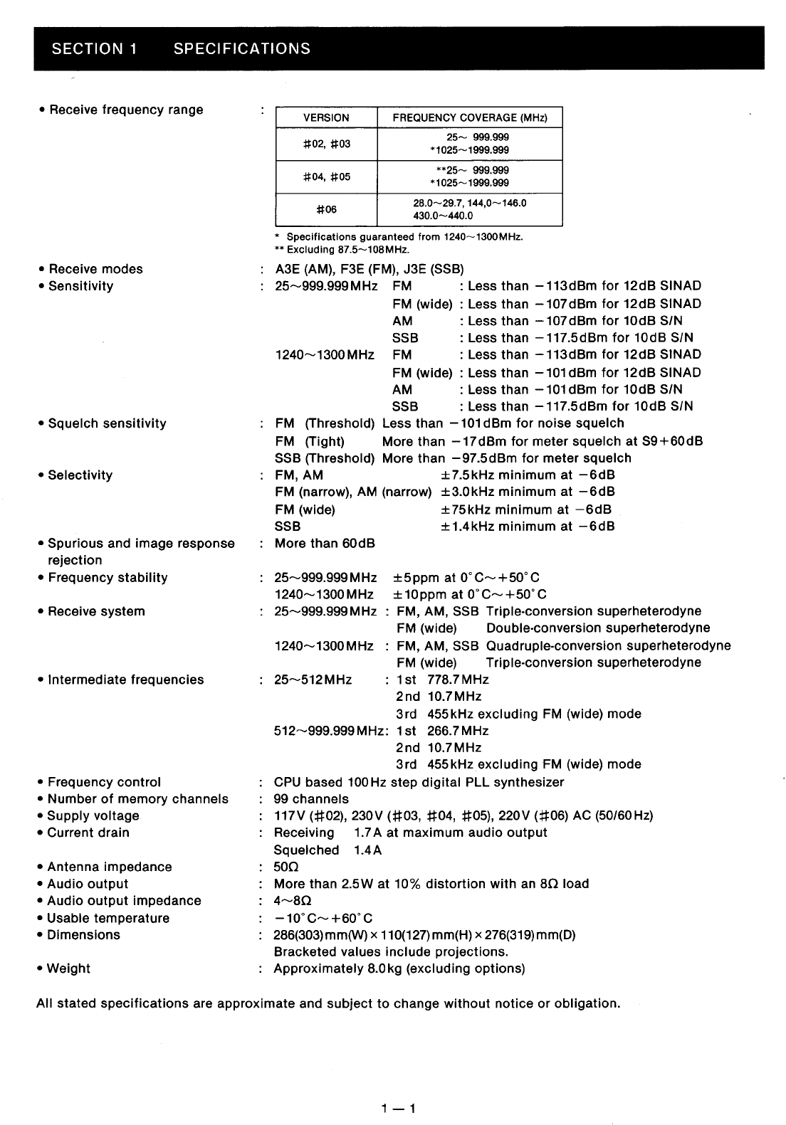
SPECIFICATIONS.......................................................
1
-1
SECTION 2 OUTSIDE AND INSIDE VIEWS . . . . . . . . . . . . . . . . . . . . . . . . . . . . . . . . . . . . . . . 2 - 1
~
4
2 - 1 FRONT PANEL . . . . . . . . . . . . . . . . . . . . . . . . . . . . . . . . . . . . . . . . . . . . . . . . . . . . . . . . . 2 - 1
2-2
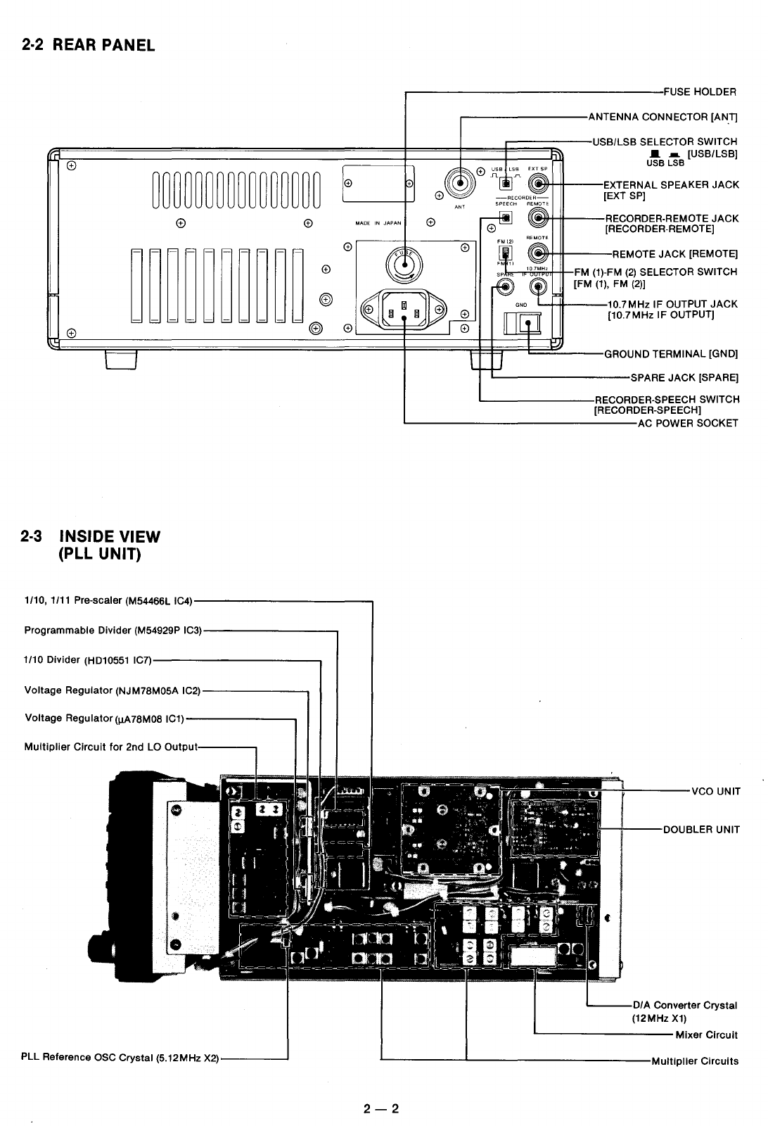
REAR PANEL
...........................................................
2-2
2 - 3 INSIDE VIEW (PLL UNIT) . . . . . . . . . . . . . . . . . . . . . . . . . . . . . . . . . . . . . . . . . . . . . . . . . 2 - 2
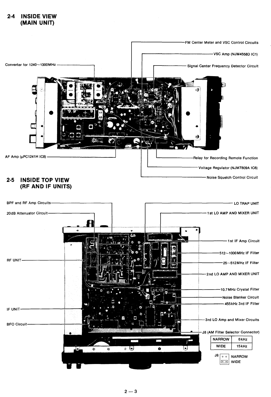
2 · 4 INSIDE VIEW (MAIN
UNIT)................................................
2 - 3
2 - 5 INSIDE TOP VIEW (RF AND IF UNITS). . . . . . . . . . . . . . . . . . . . . . . . . . . . . . . . . . . . . . 2 - 3
2 · 6 INSIDE BOTTOM VIEW (POWER SUPPLY AND DC-DC CONVERTER
UNITS)......
2 - 4
2 · 7 INSIDE BOTTOM VIEW (LOGIC UNIT) . . . . . . . . . . . . . . . . . . . . . . . . . . . . . . . . . . . . . . 2 - 4
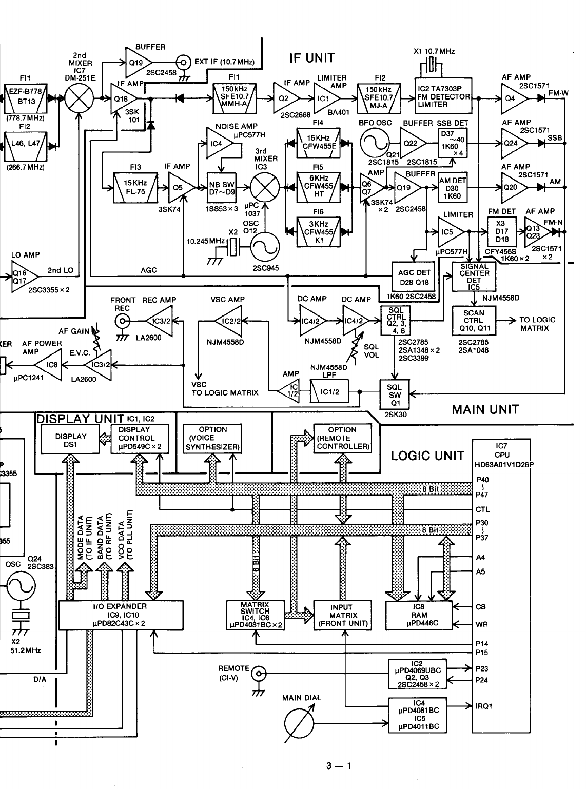
SECTION 3 BLOCK DIAGRAM . . . . . . . . . . . . . . . . . . . . . . . . . . . . . . . . . . . . . . . . . . . . . . . . . . . . . . 3 - 1
SECTION 4 CIRCUIT DESCRIPTION
.............................................
4 - 1
~
10
4 · 1 RECEIVER CIRCUITS . . . . . . . . . . . . . . . . . . . . . . . . . . . . . . . . . . . . . . . . . . . . . . . . 4 - 1 - 6
4 · 2 POWER SUPPLY CIRCUITS . . . . . . . . . . . . . . . . . . . . . . . . . . . . . . . . . . . . . . . . . . . 4 - 6
4 · 3 PLL CIRCUITS . . . . . . . . . . . . . . . . . . . . . . . . . . . . . . . . . . . . . . . . . . . . . . . . . . . . . . 4 - 7 - 8
4-
4 LOGIC
CIRCUITS....................................................
4 - 8 - 10
4 - 5 DISPLAY
CIRCUITS..................................................
4 - 10
4 - 6 KEYBOARD
CIRCUITS...............................................
4 -
10
SECTION 5 MECHANICAL PARTS AND
DISASSEMBLY...........................
5 -
1~5
5-1
FRAME DISASSEMBLY . . . . . . . . . . . . . . . . . . . . . . . . . . . . . . . . . . . . . . . . . . . . . . . . . . 5 - 1
5 - 2 FRONT PANEL
DISASSEMBLY............................................
5 - 2
5 · 3 REAR PANEL
DISASSEMBLY.............................................
5 - 3
5 · 4 TOP SIDE CONNECTOR
CONNECTIONS...
. . . . . . . . . . . . . . . . . . . . . . . . . . . . . . . . . 5 - 4
5 · 5 BOTTOM SIDE CONNECTOR CONNECTIONS . . . . . . . . . . . . . . . . . . . . . . . . . . . . . . . 5 - 5
SECTION 6 MAINTENANCE AND ADJUSTMENT
.................................
6 -
1~11
6-1
PREPARATION BEFORE
SERVICING...................................
6 - 1
6 - 2 PLL
ADJUSTMENT..................................................
6 - 2 - 3
6 · 3 LOCAL OSCILLATOR
ADJUSTMENT...................................
6 - 4 - 5
6 · 4 RECEIVER
ADJUSTMENT.............................................
6 - 6 -
11
SECTION 7 BOARD LAYOUTS . . . . . . . . . . . . . . . . . . . . . . . . . . . . . . . . . . . . . . . . . . . . . . . . . . 7 - 1
~
19
7 · 1 INTERCONNECTION
................................................
.
7 - 2 FRONT UNITS
.....................................................
.
7 · 3 MAIN UNIT
........................................................
.
7-1
7-2-3
7-4-5
7 · 4 IF
UNIT..
. . . . . . . . . . . . . . . . . . . . . . . . . . . . . . . . . . . . . . . . . . . . . . . . . . . . . . . . . . 7 - 6 - 7
7 - 5
RF
UNIT . . . . . . . . . . . . . . . . . . . . . . . . . . . . . . . . . . . . . . . . . . . . . . . . . . . . . . . . . . . 7 - 8 - 9
7 · 6 LOGIC UNIT
........................................................
7 - 10 -
11
7 · 7 PLL UNIT . . . . . . . . . . . . . . . . . . . . . . . . . . . . . . . . . . . . . . . . . . . . . . . . . . . . . . . . . . 7 -
12
-
13
7-8
DISPLAYUNIT
......................................................
7-14-15
7 - 9
REG
AND DL-REG
UNITS.............................................
7 -
16
-
17
7 ·
10
DC-DC,
EF
AND KEYBOARD UNITS . . . . . . . . . . . . . . . . . . . . . . . . . . . . . . . . . . . . 7 -
18
-
19
SECTION 8 PARTS LIST . . . . . . . . . . . . . . . . . . . . . . . . . . . . . . . . . . . . . . . . . . . . . . . . . . . . . . . . 8 - 1
~
31
SECTION 9 VOLTAGE
DIAGRAMS...............................................
9-1~4
9 - 1 IC-R7000 . . . . . . . . . . . . . . . . . . . . . . . . . . . . . . . . . . . . . . . . . . . . . . . . . . . . . . . . . . . 9 - 1 - 2
9 - 2 TV-R7000 (OPTION) . . . . . . . . . . . . . . . . . . . . . . . . . . . . . . . . . . . . . . . . . . . . . . . . . . . . . . 9 - 3
9 - 3
RC-12
(OPTION).........................................................
9 - 4
SECTION 10 SCHEMATIC DIAGRAM
.............................................
SEPARATE