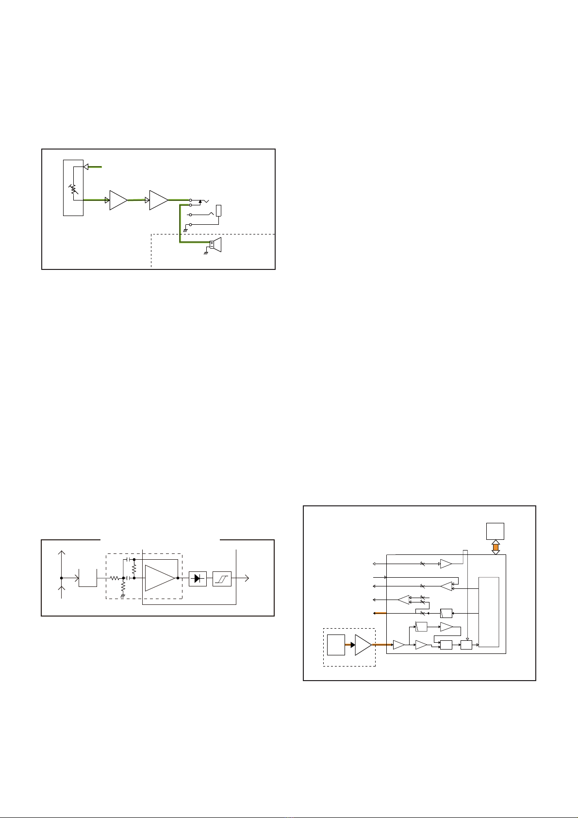
Icom IC-F6220D User manual

S-15003XZ-C1
July 2013
UHF DIGITAL TRANSCEIVER

This service manual describes the latest technical informa-
tion for the IC-F6220D UHF DIGITAL TRANSCEIVER, at the
time of publication.
NEVER connect the transceiver to an AC outlet or to a DC
power supply that uses more than the specified voltage. This
will ruin the transceiver.
DO NOT expose the transceiver to rain, snow or liquids.
DO NOT reverse the polarities of the power supply when con-
necting the transceiver.
DO NOT apply an RF signal of more than 20 dBm (100 mW) to
the antenna connector. This could damage the transceiver’s
front-end.
To upgrade quality, any electrical or mechanical parts
and internal circuits are subject to change without notice
or obligation.
MODEL VERSION VERSION
NUMBER
FREQUENCY
RANGE
IC-F6220D
USA-01 #01
400–470 MHzEXP-01 #05
CHN-01 #08
USA-02 #21 450–512 MHz
EXP-02 #25 450–520 MHz
EXP-03 #31 350–400 MHz
Be sure to include the following four points when ordering
replacement parts:
1. 10-digit Icom part number
2. Component name
3. Equipment model name and unit name
4. Quantity required
<ORDER EXAMPLE>
1110003491 S.IC TA31136FNG IC-F6220D MAIN UNIT
5 pieces
8820001210 Screw 2438 screw IC-F6220D Top cover
10 pieces
Addresses are provided on the inside back cover for your
convenience.
ORDERING PARTS
1. Make sure that the problem is internal before disassem-
bling the transceiver.
2. DO NOT open the transceiver until the transceiver is dis-
connected from its power source.
3. DO NOT force any of the variable components. Turn them
slowly and smoothly.
4. DO NOT short any circuits or electronic parts. An insulated
tuning tool MUST be used for all adjustments.
5. DO NOT keep power ON for a long time when the trans-
ceiver is defective.
6. DO NOT transmit power into a Standard Signal Generator
or a Sweep Generator.
7. ALWAYS connect a 30/50 dB to 40/60 dB attenuator be-
tween the transceiver and a Deviation Meter or Spectrum
Analyzer, when using such test equipment.
8. READ the instructions of the test equipment thoroughly
before connecting it to the transceiver.
REPAIR NOTES
INTRODUCTION CAUTION
Icom, Icom Inc. and the Icom logo are registered trademarks of Icom Incorporated (Japan) in Japan, the United States, the
United Kingdom, Germany, France, Spain, Russia and/or other countries.

TABLE OF CONTENTS
SECTION 1 SPECIFICATIONS
SECTION 2 INSIDE VIEWS
SECTION 3 DISASSEMBLY INSTRUCTION
SECTION 4 OPTIONAL CABLE INSTALLATION
SECTION 5 CIRCUIT DESCRIPITON
5-1 RECEIVER CIRCUITS...................................................................................... 5-1
5-2 TRANSMITTER CIRCUITS............................................................................... 5-2
5-3 FREQUENCY SYNTHESIZER CIRCUITS ....................................................... 5-4
5-4 VOLTAGE BLOCK DIAGRAM ........................................................................... 5-4
5-5 PORT ALLOCATIONS ...................................................................................... 5-5
SECTION 6 ADJUSTMENT PROCEDURES
6-1 PREPARATION ................................................................................................. 6-1
6-2 FREQUENCY ADJUSTMENT .......................................................................... 6-3
6-3 TRANSMIT ADJUSTMENT............................................................................... 6-4
6-4 RECEIVE ADJUSTMENT ................................................................................. 6-5
SECTION 7 PARTS LIST
SECTION 8 MECHANICAL PARTS
SECTION 9 BOARD LAYOUTS
SECTION 10 BLOCK DIAGRAM
SECTION 11 VOLTAGE DIAGRAM

1 - 1
SECTION 1
.
SPECIFICATIONS
GENERAL
• Frequency coverage [USA-01]
[EXP-01]
[CHN-01]
400–470 MHz
[USA-02] 450–512 MHz
[EXP-02] 450–520 MHz
[EXP-03] 350–400 MHz
• Type of emission Wide
Except [USA] 16K0F3E (25.0 kHz)
Narrow 11K0F3E (15.0 kHz)
8K50F3E (12.5 kHz)
Digital 4K00F1E, D (6.25 kHz)
• Number of programable channels 128 channels (8 zones)
• Output impedance (audio) 4 Ω
• Input impedance (MIC) 600 Ω
• Operating temperature range –30˚C to +60˚C (−22˚F to +140˚F)
• Power supply requirement 13.6 V DC norminal Negative ground
• Current drain
(approximately) RX Stand-by 300 mA (Digital Mode)
Maximum audio
1.2 A
TX at 45 W 11.0 A
• Dimensions 150(W)×40(H)×167.5(D) mm; 5.9(W) × 1.6(H) × 6.6(D) in
• Weight (approximately) 1.1 kg; 2 Ib 7 oz
TRANSMITTER
• Transmit output power 45 W
• Modulation Variable reactance frequency modulation
• Maximum permissible
deviation
Wide ±5.0 kHz
Narrow ±2.5 kHz
• Frequency error ±1.0 ppm
• Spurious emission [USA] 72 dB minimum 85 dB typical
[EXP], [CHN] 70 dB minimum 85 dB typical
• Adjacent channel power Wide 70 dB minimum 73 dB typical
Narrow
Digital 60 dB minimum 70 dB typical
• Audio harmonic distortion 3% typical (with 1 kHz AF 40% deviation)
• FM hum and noise
(without CCITT filter)
Wide 40 dB minimum 46 dB typical
Narrow 34 dB minimum 40 dB typical
• Limiting charact of modulation 70–100% of maximum deviation
• Microphone impedance 2.2 kΩ
RECEIVER
• Receive system Double conversion superheterodyne
• Intermediate frequencies 1st IF; 46.35 MHz, 2nd IF; 450 kHz
• Sensitivity 0.25 μV typical at 12 dB SINAD
–8 dBμV (EMF) typical at 5% BER
• Squelch sensitivity (at threshold) 0.25 μV typical
• Adjacent channel
selectivity
Wide 70 dB minimum 75 dB typical
Narrow 65 dB minimum 68 dB typical
Digital 50 dB minimum 60 dB typical
• Spurious response More than 70 dB
• Intermodulation Wide
Narrow 70 dB minimum 75 dB typical
Digital 65 dB minimum 70 dB typical
• Hum and Noise
(without CCITT filter)
Wide 40 dB minimum 46 dB typical
Narrow 34 dB minimum 40 dB typical
• Audio output power 4.0 W typical at 5% distortion with an 4 Ωload
All stated specifications are subject to change without notice or obligation.

2 - 1
SECTION 2
.
INSIDE VIEWS
• FRONT UNIT
(BOTTOM VIEW)
CPU
(IC51)
EEPROM
(IC52)
LCD DRIVER
(IC6)
MIC AMP
(IC7)
LIGHT CTRL
(Q5)
CLOCK FREQUENCY
SHIFT DIODE
(D60)
DIM CTRL
(Q1)
DIM CTRL
(Q2)

2 - 2
• MAIN-A/-B/-C UNIT
(TOP VIEW)
POWER SW
(Q1001)
APC AMP
(IC2)
POWER SW
(Q1003)
XTAL BPF
(DIGITAL)
(FI5)
XTAL BPF
(ANALOG)
(FI4)
+3V REGULATOR
(Q1017)
IF AMP
(Q14)
DSP
(IC2007)
CERAMIC BPF
(FI3)
IF IC
(IC4)
MIC AMP
(IC7)
BUFFER
(Q3)
BUFF
(Q5)
RIPPLE FILTER
(Q17)
VCO SW
(Q15)
+8V REGULATOR
(IC1002)
R8 REGULATOR
(Q1013)
MUTE SW
(Q6)

3 - 1
SECTION 3
.
DISASSEMBLY INSTRUCTION
FLAT
CABLE
BOTTOM COVER
FRONT PANEL
SPEAKER
CABLE
MAIN UNIT
FILTER
CASE
EARTH
SPRING
UNSOLDER
Solder
remover
UNSOLDER
Solder
remover
MAIN UNIT
MAIN UNIT
1) Unscrew 4 screws from the bottom cover, and remove the
bottom cover.
2) Disconnect the flat cable and speaker cable.
3) Unscrew 2 screws from the both sides, and remove the
front panel in the direction of the arrow.
5) Unscrew 9 screws and remove the filter case and the
earth spring from the MAIN UNIT.
6) Unsolder total of 7 points; 3 points at the antenna
connector, 4 points at the PA module.
7) Take off the MAIN UNIT from the CHASSIS.
4) Unsolder 2 points.

4 - 1
SECTION 4 OPTIONAL UNIT INSTALLATION
Install optional OPC-1939 as follows;
1) Turn the transceiver OFF, then disconnect the DC power
cable.
2) Unscrew 4 screws, then remove the bottom cover.
3) Install the cable as shown below.
OPC-1939
Cut off the bushing as in the illustration,
when you install the optional OPC-1939.
K
I
4) Cut or short the patterns as below. (For AF output)
6) Recover the bottom cover, screws and DC power cable.
NOTE: Be sure to recover the patterns when you remove the optional product. Otherwise no TX modulation or AF output is available.
Solder
remover
D
5) Short the pattern as below. (For modulation input)

5 - 1
SECTION 5
.
CIRCUIT DESCRIPTION
X3
Q4
BPF
X2
TCXO
W/N
SW
D2,D3
BPF
CERAMIC
FI2
BPF
CERAMIC
FI1
W/N
SW
D8,D9
IF IC
From the 1st IF
circuits
IC4
15.3MHz
45.9MHz
450kHz
450kHz
AMP
BUFF BPF
CERAMIC A/D
AMP
HPF
ALC
AMP
BUFF
LPF
BUFF
LIMIT
AMP
BUFF
IC5 2002CI
3I
F
5Q
MOD
LINE
CTRL
DIF
IC2007
De-Emphasis
Signaling
Decode
DAFO
SW
IC1010
VCON REF
TX/RX
AFVO
BEEP
SQIN
DET
MOD DMO
BAL
BDR0
BCLKR0
BFSR0
BCLKX1
MICI
BFSX1
BDX1
BDR1
DSP
CODEC
LINEAR
5-1 RECEIVER CIRCUITS
RF CIRCUIT
The RX signal from the antenna is passed through the
LPF(L1–L3, C1, C2, C4–C8, and C404) and antenna SW
(D5, D24), and then filtered by the 2-staged tuned BPFs
(D4, D21–D22) to eliminate unwanted out-of-band signals.
The filtered RX signal is amplified by the RF AMP (Q2), and
filtered by 2-staged tuned BPF (D10, D19) to obtain a good
image response, then applied to the 1st IF circuits.
The BPFs are tuned to the RX frequency by applying ad-
equate tuning voltages: “T1” and “T2” to the variable capaci-
tors.
• RF CIRCUIT
1ST IF CIRCUIT
The RX signal from the RF circuits is applied to the 1st IF
mixer (Q19) and mixed with the 1st LO signal from the RX
VCO, resulting in the 46.35 MHz 1st IF signal. The 1st IF sig-
nal is passed through the IF SWs (D13, D14, D17, D18) and
the crystal filter (FI4: analog mode, FI5: digital mode) to be
filtered, amplified by the 1st IF AMP (Q14), and then applied
to the 2nd IF circuits.
• 1ST IF CIRCUIT
2ND IF AND DEMODULATOR CIRCUITS
The signal from the 1st IF circuits is applied to the IF demod-
ulator IC (IC4) which contains the 2nd IF mixer, 2nd IF AMP,
FM detector, squelch circuit and AF AMP in its package.
The 1st IF signal is applied to the 2nd IF mixer and mixed
with the 2nd LO signal resulting in the 450 kHz 2nd IF signal.
The 2nd LO signal is generated by tripling the 15.3 MHz
reference frequency signal generated by the reference fre-
quency oscillator (TCXO; X2).
• WHILE OPERATING IN THE ANALOG MODE
The 2nd IF signal is filtered by the 2nd IF filter (FI2: wide
mode) or filters (FI1 and FI2: narrow) to eliminate unwanted
signals. It is amplified by the 2nd IF AMP, and then demodu-
lated by the detector circuit, which employs the discriminator
(X1) as the phase shifter.
The demodulated AF signal is applied to the linear codec
(
inside the AF CUSTOM IC (IC1010)). The AF signal is
encoded into a digital signal, then demodulated by DSP
(IC2007). The demodulated signal is then applied to the
linear codec
(
inside the AF CUSTOM IC (IC1010)) to be de-
coded into an analog audio signal.
• WHILE OPERATING IN THE DIGITAL MODE
The 2nd IF signal is filtered by the 2nd IF filters (FI1 and FI2)
to eliminate unwanted signals, and applied to the IF AMP
(IC5) through the buffer (Q5). The amplified 2nd IF signal is
passed through the ceramic filter (FI3), and then applied to
the A/D converter (IC2002) to be encoded into a digital sig-
nal. The digital signal is demodulated by the DSP (IC2007),
and then applied to the linear codec
(
inside the AF CUSTOM
IC (IC1010)) to be decoded into an analog audio signal.
The AF signal is applied to the RX AF circuits.
• 2ND IF AND DEMODULATOR CIRCUITS
LPF
ANT
SW
RF
AMP
Q2 D20, D22
BPFBPF
D10
T2
BPF
D19
T2 T1
D4,D21
BPF
T1
From the TX circuits
To the 1st
IF circuits
ANT
D5,D24
LO
SW
D5,D6
D17,D18D13,D14
Q19
BPF
XTAL
FI4
IF
AMP
Q14
BUFF
Q8
BUFF
Q10
ATT
IF SW
IF SW
RX VCO
To the TX circuits
From the RF circuits
e
2nd IF circuits
46.35MHz
BPF
XTAL
FI5
46.35MHz
1st IF mixer

5 - 2
RX AF CIRCUITS
The detected audio signals adjusted by the linear codec’s
electoronic volume (inside the AF CUSTOM IC (IC1010)).
The level-adjusted AF signal is then amplified by the pre-
AMP (IC1004) and AF power AMP (IC1009).
The power amplified AF signal is passed through the exter-
nal speaker jack (J1002), and then applied to the internal
speaker.
• RX AF CIRCUIT
SQUELCH CIRCUIT (Analog mode only)
The squelch circuit cuts off the AF output signals when no
RF signals are received. Detecting noise components in the
demodulated AF signals, the squelch circuit stops audio sig-
nals being heard.
A portion of the demodulated AF signal from the IF IC (IC4)
is passed through the AF CUSTOM IC (IC1010) for level
(=threshold) adjustment. The level-adjusted AF signals are
passed through the noise filter (IC4, pins 7, 8 and Q9, R42,
R44–R45, C68–C70) to filter only the noise components (ap-
proximately 30 kHz signals). The noise components are rec-
tified, resulting in a DC voltage corresponding to the noise
level.
If the noise level is higher than the preset one, the internal
comparator set the “NOISE” signal to the CPU to “High,” then
the CPU turns the “AFON” signal, which controls the AF
mute SW, (Q1008, Q1012, D1007) to “Low,” to stop the AF
output.
• SQUELCH CIRCUIT
AF
AMP
AF
AMP
IC1009 J4
SP1
Int.speaker
Ext.speaker
From the IF IC
IC1004
AFO
AFVO
Electronic
volume
FRONT UNIT
IC1010
DAC Noise
AMP
Noise filter
From IF IC
(IC4, Pin16)
To RX AF circuits
Noise
detector
Com-
parator
NOISE SQUELCH DIAGRAM
“NOIS”
IC1006
IC4
14
8
7
13
15
J1
FRONT UNIT
[MIC
JACK] AMP
IC7
DSP
IC2007
AMP
HPF
ALC
AMP
BUFF
LPF
BUFF
LIMIT
AMP
BUFF
MOD
LINE
CTRL
DAFO
SW
IC1010
VCON REF
TX/RX
AFVO
BEEP
SQIN
MOD DMO
BAL
MICI
CODEC
LINEAR
5-2 TRANSMITTER CIRCUIT
TX AF CIRCUIT
The audio signal from the microphone (MIC signal) is passed
through the MIC AMP (IC7), and then applied to the AF CUS-
TOM IC (IC1010).
• WHILE OPERATING IN THE ANALOG MODE
The amplified MIC signal is passed through the HPF (inside
the AF CUSTOM IC (IC1010, pin 3)), which attenuates fre-
quencies 300 Hz and below, and then applied to the limiter
AMP
(inside the AF CUSTOM IC (IC1010
, pin 4)).
The am-
plitude-limited MIC signal is applied to the AF CUSTOM IC
(inside the IC1010).
The MIC signal is converted into a digital audio signal by
the linear codec (inside the AF CUSTOM IC (IC1010)), pro-
cessed by the DSP (IC2007), and then converted into an
analog baseband signal (modulation signal).
• WHILE OPERATING IN THE DIGITAL MODE
The amplified MIC signal is applied to the ALC (inside the AF
CUSTOM IC (IC1010, pin10)) which keeps the signal level
fixed.
The level-adjusted MIC signal is
applied to the linear codec
(
inside the AF CUSTOM IC (IC1010)) through the MIC line
SW (inside the AF CUSTOM IC (IC1010)).
The MIC signal is converted into a digital audio signal by
the linear codec (inside the AF CUSTOM IC (IC1010)), pro-
cessed by the DSP (IC2007), and then converted into the
digital baseband signal (modulation signal).
The signal from the linear codec (inside the AF CUSTOM IC
(IC1010)) is passed through the LPF (inside the AF CUS-
TOM IC (IC1010)), and then applied to the D/A converter
(inside the AF CUSTOM IC (IC1010))
which adjusts its level
(=deviation)
.
The level-adjusted modulation signal is applied to the modu-
lation circuit.
• TX AF CIRCUIT

5 - 3
LO
SW
D25
Q13,D6
MODULATION
D26
BUFF
Q10
BUFF
Q11
TX VCO
From the TX AF circuits
To the TX AMP circuits
MOD
LPF
PWR
DET
D1,D11,D12
MUTE
SW
Q6
ANT
SW
D3,D5,D6,D68
PWR
AM P
IC3
APC
AMP
IC2
DRIVE
AMP
Q8
TMUT
ANT
From the TX VCO
To the RX circuits
LPF
LPF
LO
SW
D14,D15
Q24,D33
Q23,D16
FILTER
LOOP
PLL
IC
SO,SCL,PLST
IC3
X3
Q4
Q3
To the TX AMPs
BPF
BUFF
Q10
BUFF
Q11
BUFF
Q12
X2
TCXO
LV
ADJ
D64
LV
ADJ
D62
ATT
IF IC
RX VCO
TX VCO
IC4
VCON
15.3MHz
45.9MHz
1st IF mixer
LV
LVA
Transmit circuits
Receive circuits
TX/RX common circuits
VCOs and LO buffers
AF power AMP
Logic circuits
CPU
+3
REG
Q1017,Q1019
+8
REG
IC1002
+5
REG
Q1014,Q1015
+3
REG
IC1001
W2
SW
POWER
Q1003
Q1001
T8
REG
Q1013,Q1016
R8
REG
+3.3V
RXC
CPU3.3V
R8V
VCC
PWON
8V
8V
VCC
8V
VCC
8V
+5V
TXC
8V
T8V
HV
VCC
D1008,Q1011,
Q1018,Q1021
5-4 VOLTAGE DIAGRAMS
MODULATION CIRCUITS
The modulation signal from the TX AF circuits is applied to
D26 of the TX VCO (Q23, D16, D26, D64) to modulate it (FM
for the analog mode, 4FSK for the digital mode). The modu-
lated signal from the TX VCO is buffer-amplified by two buf-
fers (Q11, Q10), and applied to the TX AMP circuits through
the LO SW (D25).
• MODULATION CIRCUIT
TX AMPLIFIER
The buffer amplified signal from the LO SW (D25) is se-
quentially amplified by the pre-drive AMP (Q25), drive AMP
(Q8) and power AMP (IC3), to obtain TX power. The ampli-
fied TX signal is passed through the antenna SW (D5, D24)
and the LPFs, which eliminates harmonics, and then applied
to the antenna.
APC CIRCUIT
D11, D12 and D29 rectify a portion of the TX signal to direct
current, and the APC AMP (IC2) compares the voltage and
the TX power control reference voltage, “T1.” The resulting
voltage controls the gain of the power AMP (IC3) to keep the
TX power constant.
• TX AMPLIFIERS AND APC CIRCUIT
5-3
FREQUENCY SYNTHESIZER CIRCUIT
The RX VCO is composed of Q24, D33 and D62. The VCO
output signal is buffer-amplified by two buffers (Q11 and
Q10), and then applied to the 1st IF mixer, through the LO
SW (D15) and the attenuator.
The TX VCO is composed of Q23, D16, D26 and D64. The
VCO output signal is buffer-amplified by two buffers (Q11
and Q10), and then applied to the pre-drive AMP (Q25),
through the LO SW (D25) and the LPF.
A portion of signal generated by each VCO is fed back to the
PLL IC (IC8, pin 17), through the buffer (Q12) and the LPF
(L13, C298–C300).
The applied VCO output signal is divided and phase-com-
pared with a 15.3 MHz reference frequency signal from the
TCXO (X2), which is also divided. The resulting signal is
output from the PLL IC (IC3), and DC-converted by the loop
filter, and then applied to the VCO as the lock voltage.
When the oscillation frequency drifts, its phase changes
from that of the reference frequency, causing a lock voltage
change to compensate for the drift in the VCO oscillating fre-
quency.
• FREQUENCY SYNTHESIZER CIRCUIT

5 - 4
5-5 PORT ALLOCATIONS
• CPU (FRONT UNIT: IC51)
BALL
No.
LINE
NAME DESCRIPTION I/O
A1 KR1 [P1] input. I
A5 RXC Power supply switching control.
H= During receive or stand-by. O
A7 TDAT Serial data to the DSP (IC2007). O
A15 PWON Power supply switching control.
H= The transceiver's power is ON. O
B1 KR3 [P3] input. I
B2 KR0 [P0] input. I
B12 NOIS Noise level detect.
H= Squelch close I
B13 EPTT External PTT input.
H= An external PTT is pushed. I
B14 PGIO4 External I/O port. I/O
B15 AFON AF mute SW control.
H= During the squelch circuit is opened. O
C3 KR2 [P2] input. I
C5 TXC Power supply switching control.
H= While transmitting. O
C8 ESDA EEPROM (IC52) serial data. I/O
C12 POSW []input. I
C14 ADS
1st IF filters (FI4 and FI5) switching
control.
L= During digital mode.
O
C15 NWC
Receive mode (narrow/mid/wide)
switching.
L= During narrow mode.
O
D6 DSCK DSP (IC2007) clock. O
D8 ESCL EEPROM (IC52) clock. O
D13 DPDN DSP (IC2007) power control.
H= DSP is inactivated O
D14 DRES DSP (IC2007) reset.
L= Reset O
D15 CSFT Clock frequency shift.
H= Clock frequency is shifted. O
E13 CRES CPU reset. I
H1 SIDE1 [ ] key input.
L= Pushed I
H2 SIDE2 []key input.
L= Pushed I
J1 IPTT Microphone [PTT] input.
L= Pushed. I
K3 LIGT1 LCD dimmer control.
H= Dimmer OFF. O
L1, L2 MCG0,
MCG1 MIC gain control. O
L3 LIGT2 Backlight control.
H= Backlight ON. O
L4 HANG Microphone hang up detection. I
L14 SSO Common serial data. O
L15 SCK Common clock. O
M1 TMUT Transmission mute.
L= TX inhibit. O
M8 BEEP Beep audio. (Square waves) O
M14 DAST D/A converter (IC1006) strobe.
H= Load enable. O
N2 LINH LCD driver (IC6) chip enable.
H= Enable. O
N4 UNLK PLL (IC8) unlock detect.
L= Unlocked. I
N12 BATV Power supply voltage sensing. I
BALL
No.
LINE
NAME DESCRIPTION I/O
N14 RDAT DSP (IC2007) serial data. O
N15 IGSW Ignition SW detect.
L=Ignition detected. I
P1 LCK LCD driver (IC6) clock. O
P2 LCS LCD driver (IC6) chip select. O
P4 PLSW PLL lock up time control.
L= Fast lock up O
P10 TEMP Temperature sensing voltage. I
P11 RSSI RSSI sensing voltage. I
P12 AFVI [VOLUME CONTROL] input. I
R1 LSO LCD driver (IC6) serial data. O
R4 PLST PLL strobe. O
R10 LVIN Lock voltage input. I

6 - 1
SECTION 6
.
ADJUSTMENT PROCEDURE
Modulation analyzer
(DC measurable)
Attenuator
50 dB or 60 dB
to the antenna connector
to DC cable
Standard signal generator
–127 to –17 dBm
(0.1 V to 32 mV)
CAUTION:
DO NOT transmit while
SSG is connected to
the antenna connector.
RF power meter
60 W
DC power supply
13.6 V / 20 A
Frequency
counter
Oscilloscope
AC millivoltmeter
Audio generator
to the MIC
connector
JIG CABLE
to USB port
PC
M CONNECTION
M JIG CABLE
6-1 PREPARATION
EQUIPMENT GRADE AND RANGE EQUIPMENT GRADE AND RANGE
Cloning Software CS-F3210D/
F3230D/F5220D : Revision 1.0 or later JIG Cable
Modified OPC-1122U (see the illust below)
DC Power Supply Output voltage
Current capacity
: 13.6 V DC
: More than 20 A Attenuator Power attenuation
Capacity
: 50 or 60 dB
: 60 W or more
Modulation
Analyzer
Frequency range
Measuring range
: DC–600 MHz
: 0 to ±10 kHz External Speaker Input impedance
Capacity
: 4 Ω
: 20 W or more
Frequency Counter
Frequency range
Frequency accuracy
Sensitivity
: 0.1–600 MHz
: ±1 ppm or better
: 100 mV or better
Standard Signal
Generator (SSG)
Frequency range
Output level
: 0.1–600 MHz
: 0.1 µV to 32 mV
(–127 to –17 dBm)
RF Power Meter
Measuring range
Frequency range
Impedance
SWR
: 0.1–60 W
: 100–600 MHz
: 50 Ω
: Better than 1.2 : 1
Oscilloscope Frequency rang
Measuring range
: DC–20 MHz
: 0.01–20 V
Add a jumper wire here
OPC-1122U
+
GND
MIC
PTT
GND
GND
SP
PTT SWITCH
+−
AC MILLIVOLTMETER
(10 mV to 10 V)
AUDIO GENERATOR
(300–3000 Hz/1–500 mV)
+−
+−
4.7 µF
EXT. SPEAKER
(5 W/4 Ω)
SETTING;
Frequency : 1 kHz
Level : 40 mVrms
Waveform : Sine wave

6 - 2
M ADJUSTMENT CHANNELS
• For [High band] version
• For [Low band] version

6 - 3
• For [350 MHz band] version
CONVENIENT: The same cloning file is available.
Right-click below, and select "Save Embeded File to
Disk."
For [Low band] version:
For [High band] version:
For [350 MHz band] version:

6 - 4
M ADJUSTMENT UTILITY
ADJUSTMENT CONDITION
REFERENCE FREQUENCY
TX OUTPUT POWER
SQUELCH
SENSITIVITY
PLL LOCK VOLTAGE (RX)
PLL LOCK VOLTAGE (TX)
CTCSS DEVIATION
DTCS DEVIATION
MODULATION BALANCE
MODULATION BALANCE
(PRESET)
DIGITAL DEVIATION
FM DEVIATION
S-METER
2/5 TONE DEVIATION

6 - 5
• I/O Check screen
(The values shown above are exsample only.
Each transceiver has own values.)
Lock voltage
appears here
* * *
ADJUSTMENT TRANSCEIVER’S
CONDITION OPERATION ADJUSTMENT
ITEM VALUE
PLL LOCK
VOLTAGE
(RX)
1 • Channel : 1-1
• Receiving
• Connect an RF power meter to the
antenna connector.
[RX LVA(Adjust)] 1.0 V
2 • Channel : 1-2
• Receiving [RX LVA(Check)] 3.95–4.05 V
(TX) 3 • Channel : 1-1
• Transmitting [TX LVA(Adjust)] 1.0 V
4• Channel : 1-2
• Transmitting [TX LVA(Check)] 3.95–4.05 V
REFERENCE
FREQUENCY
1 • Channel : 1-2
• Transmitting
• Loosely couple a frequency counter to the
antenna connector. [REF]
470.000000 MHz*
520.000000 MHz**
400.000000 MHz***
(±100 Hz)
*; [Low band] versions.
**; [High band] versions.
***; [350 MHz band] versions.
6-2 FREQUENCY ADJUSTMENTS
1) Select an adjustment item using [↑]/[↓] on the PC's keyboard.
2) Set or modify the adjustment value as specified using [←]/[→] on the PC's keyboard, then push [ENTER].

6 - 6
No over or under shoot.
As flat as possible.
ADJUSTMENT TRANSCEIVER’S
CONDITION OPERATION ADJUSTMENT
ITEM VALUE
TX OUTPUT
POWER
(High power)
1 • Channel : 1-3
• Transmitting
• Connect an RF power meter to the
antenna connector. [Power (Hi)]
45 W
(L2 power) 2 • Channel : 1-4
• Transmitting [Power (L2)] 25 W
(L1 power) 3 • Channel : 1-5
• Transmitting [Power (L1)] 4.5 W
MODULATION
BALANCE
-Band low-
1•Set [TX MODE] to "2 (Analog 100Hz Pulse)" on the "Adjust
Utility” screen. [TX MODE] 2
(Analog 100Hz Pulse)
3•Push [ENTER] on the PC’s keyboard, to enter the modulation
balance adjustment mode. [BAL Start] –
4 • Channel : 1-6
• Transmitting
• Connect a modulation analyzer with an
oscilloscope to the antenna connector,
through an attenuator, and then set it as;
HPF : OFF
LPF : 15 kHz
De-emphasis : OFF
Detector : (P–P)/2
[BAL 1]
Square waveform
-Band center- 5 • Channel : 1-7
• Transmitting [BAL 2]
-Band high- 6 • Channel : 1-8
• Transmitting [BAL 3]
7•Push [ENTER] on the PC’s keyboard, to store the value and
quit the modulation balance adjustment mode. [BAL Start] –
FM DEVIATION
(Narrow mode)
-Band low-
1•Push [ENTER] on the PC’s keyboard, to enter the FM deviation
(For narrow mode) adjustment mode. [MOD N Start] –
2 • Channel : 1-9
• Transmitting
• Connect a modulation analyzer to the
antenna connector, through an attenuator,
and set it as described in the "MODULATION
BALANCE" above.
• Connect as audio generator to the [MIC]
jack, and set it as;
Frequency : 1 kHz (Sine wave)
Level : 40 mVrms
[MOD N L]
±2.10 ±0.05 kHz
-Band center- 3 • Channel : 1-10
• Transmitting [MOD N C]
-Band high- 4 • Channel : 1-11
• Transmitting [MOD N H]
5•Push [ENTER] on the PC’s keyboard, to store the value and
quit the FM deviation (For narrow mode) adjustment mode. [MOD N Start] –
(Wide mode)†
-Band low-
6•Push [ENTER] on the PC’s keyboard, to enter the FM deviation
(For wide mode) adjustment mode. [MOD W Start] –
7 • Channel : 1-12
• Transmitting
•
Connect a modulation analyzer to
the antenna connector, through an
attenuator, and set it as described in the
"MODULATION BALANCE" above.
• Connect as audio generator to the [MIC]
jack, and set it as;
Frequency : 1 kHz (Sine wave)
Level : 40 mVrms
[MOD W L]
±4.20 ±0.05 kHz
-Band center- 8 • Channel : 1-13
• Transmitting [MOD W C]
-Band high- 9 • Channel : 1-14
• Transmitting [MOD W H]
10 • Push [ENTER] on the PC’s keyboard, to store the value and
quit the FM deviation (For wide mode) adjustment mode. [MOD W Start] –
†; For all models except [USA]
6-3 TRANSMIT ADJUSTMENTS
1) Select an adjustment item using [↑]/[↓] on the PC's keyboard.
2) Set or modify the adjustment value as specified using [←]/[→] on the PC's keyboard, then push [ENTER].

6 - 7
6-3 TRANSMIT ADJUSTMENTS (continued)
1) Select an adjustment item using [↑]/[↓] on the PC's keyboard.
2) Set or modify the adjustment value as specified using [←]/[→] on the PC's keyboard, then push [ENTER].
ADJUSTMENT TRANSCEIVER’S
CONDITION OPERATION ADJUSTMENT
ITEM VALUE
DIGITAL
DEVIATION
(Band Low)
1•Set [TX MODE] to "16 (Digital Max Amp 600Hz Sin Wave)" on
the "Adjust Utility” screen. [TX MODE]
16
(Digital Max Amp
600Hz Sin Wave)
2•Push [ENTER] on the PC’s keyboard, to enter the digital
deviation adjustment mode. [MOD D Start] –
3 • Channel : 1-15
• Transmitting
• Connect a modulation analyzer to
the antenna connector, through an
attenuator, and set it as;
HPF : OFF
LPF : 15 kHz
De-emphasis : OFF
Detector : (P–P)/2
[MOD D L] ±1.37 ±0.02 kHz
(Band Center) 4 • Channel : 1-16
• Transmitting [MOD D C]
(Band High) 5 • Channel : 1-17
• Transmitting [MOD D H]
6•Push [ENTER] on the PC’s keyboard, to store the value and quit
the digital deviation adjustment mode. [MOD D Start] –
CTCSS
DEVIATION
1 • Channel : 1-18
• Transmitting
1) Set the TX Mode to "3" on the "Adjust
Utility" screen.
2) Connect a modulation analyzer to
the antenna connector through an
attenuator, and set it as described in
the "DIGITAL DEVIATION" above.
[CTCSS]
±0.35 ±0.05 kHz
DTCS
DEVIATION
1 • Channel : 1-19
• Transmitting
1) Set the TX Mode to "4" on the "Adjust
Utility" screen.
2) Connect a modulation analyzer to
the antenna connector through an
attenuator, and set it as described in
the "DIGITAL DEVIATION" above.
[DTCS]
REFERENCE
FREQUENCY
1 • Channel : 1-20
• Transmitting
• Loosely couple a frequency counter to
the antenna connector. [REF]
470.000000 MHz*
520.000000 MHz**
400.000000 MHz***
(±200 Hz)
*; [Low band] versions.
**; [High band] versions.
***; [350 MHz band] versions.

6 - 8
6-4 RECEIVE ADJUSTMENTS
1) Select an adjustment item using [↑]/[↓] on the PC's keyboard.
2) Set or modify the adjustment value as specified using [←]/[→] on the PC's keyboard, then push [ENTER].
ADJUSTMENT TRANSCEIVER’S
CONDITION OPERATION ADJUSTMENT
ITEM VALUE
RX SENSITIVITY 1NOTE: When "RX SENSITIVITY" is re-adjusted, "S-METER" must be re-adjusted too.
• Channel : 1-21
• Receiving
• Set the SSG to the antenna connector and
set it as;
Frequency : 400.000 MHz*
450.000 MHz**
350.000 MHz***
Level†: +20 dBµ (–87 dBm)
Modulation : 1 kHz
Deviation : ±1.5 kHz
[BPF C ALL]
Push
[ENTER].
RSSI
(S3 level setting)
1NOTE: When "RX SENSITIVITY" must be adjusted before "S-METER." And when "RX SENSITIVITY"
is re-adjusted, "S-METER" must be re-adjusted too.
• Channel : 1-22
• Receiving
• Connect the SSG to the antenna connec-
tor and set as;
Frequency : 400.000 MHz*
450.000 MHz**
350.000 MHz***
Level†: +23 dBµ (–84 dBm)
Modulation : None
[RSSI S3 Level]
Push
[ENTER].
(S3 level setting) 2•Set the SSG to the antenna connector and
set it as;
Frequency : 400.000 MHz*
450.000 MHz**
350.000 MHz***
Level†: –7 dBµ (–114 dBm)
Modulation : None
[RSSI S1 Level]
SQUELCH 1NOTE: When "RX SENSITIVITY" must be adjusted before "SQUELCH." And when "RX SENSITIVITY"
is re-adjusted, "SQUELCH" must be re-adjusted too.
• Channel : 1-23
• Receiving
• Set the SSG to the antenna connector and
set it as;
Frequency : 470.000 MHz*
520.000 MHz**
400.000 MHz***
Level†: –14 dBµ (–121 dBm)
Modulation : 1 kHz
Deviation : ±1.50 kHz
2) Once close the squelch by increasing [SQL]
value, then decrease the value to open the
squelch.
––
2[SQL] Push
[ENTER].
†; The output level of the standard signal generator (SSG) is indicated as the SSG’s terminated circuit (emf).
*; [Low band] versions.
**; [High band] versions.
***; [350 MHz band] versions.
Table of contents
Other Icom Transceiver manuals

Icom
Icom IC-M36 User manual

Icom
Icom IC-4SA User manual

Icom
Icom IC-720A User manual

Icom
Icom IC-F4162DS User manual

Icom
Icom IC-F4261DT User manual

Icom
Icom IC-M601 User manual

Icom
Icom IC-2GA User manual

Icom
Icom IC-F24/S Installation and operating instructions

Icom
Icom IC-901A User manual

Icom
Icom IC-4A User manual