IDT ZMID5201 User manual

ZMID520x User Guide for Getting Started
© 2018 Integrated Device Technology, Inc.
1
April 6, 2018
Contents
1. Introduction...................................................................................................................................................................................................3
2. Inductive Sensing Technology Introduction..................................................................................................................................................3
2.1 Device Block Diagram .........................................................................................................................................................................6
3. Getting Started .............................................................................................................................................................................................7
3.1 LC Tank –Tx Front-End Tuning ..........................................................................................................................................................7
3.2 Device Initialization..............................................................................................................................................................................8
3.2.1 Output Mode Selection .........................................................................................................................................................8
3.3 Offset Check for Rx Coils ....................................................................................................................................................................9
3.4 Gain Stage Setting ............................................................................................................................................................................11
3.5 Input Amplitude Offset Compensation...............................................................................................................................................12
3.6 Output Calibration..............................................................................................................................................................................13
3.7Output Linearization ..........................................................................................................................................................................14
4. Internal Memory..........................................................................................................................................................................................17
5. Programming the ZMID520x EEPROM......................................................................................................................................................19
6. Glossary .....................................................................................................................................................................................................19
7. Revision History..........................................................................................................................................................................................20
List of Figures
Figure 1. Tx Loop Magnetic Field .......................................................................................................................................................................3
Figure 2. Current Paths and Shapes for Coils –Example for Linear Position Sensing ......................................................................................4
Figure 3. Geometrical Illustration for Coils and Target –Example for Linear Position Sensing..........................................................................5
Figure 4. Main Internal Functional Block Diagram..............................................................................................................................................6
Figure 5. ZMID520x Transmitter LC Tank..........................................................................................................................................................7
Figure 6. TX Oscillation and LF-U 5 Probe.........................................................................................................................................................8
Figure 7. ZMID520x EEPROM Memory Values –ZMID5203 Example for the Linear Output Mode Settings ..................................................9
Figure 8. ZMID520x EEPROM Gain Stage Setting –Example using the ZMID5203........................................................................................9
Figure 9. Coil Offset Reading –Example using the ZMID5203........................................................................................................................10
Figure 10. Magnitude for Gain Selection –Example for the ZMID5203 .............................................................................................................11
Figure 11. ZMID520x Input Amplitude Offset Compensation –Example for the ZMID5203 ..............................................................................12
Figure 12. Output Calibration..............................................................................................................................................................................13
Figure 13. Output Calibration Verification...........................................................................................................................................................14
Figure 14. Correction Mode Selection ................................................................................................................................................................14
Figure 15. Measured Value Readings for 9 Linearization Points........................................................................................................................15
Figure 16. Input Fields for the 9 Linearization Points Measured Values.............................................................................................................16
Figure 17. ZMID520x Internal Memory ...............................................................................................................................................................17

ZMID520x User Guide for Getting Started
© 2018 Integrated Device Technology, Inc.
2
April 6, 2018
List of Tables
Table 1. EEPROM and Shadow RAM Contents..............................................................................................................................................17
ZMID520x User Guide for Getting Started
© 2018 Integrated Device Technology, Inc.
3
April 6, 2018
1. Introduction
This document describes the procedures for setting up the IDT ZMID520x internal memory and transmitter (Tx) front-end in order to start
measurements with the device in user applications. It describes the settings needed to prepare the device for operation and then gives an
internal memory overview.
The steps provided here are needed when configuring a new device in a user application. These procedures can also be applied to any of the
ZMID520x application modules provided by IDT; however this is typically not needed because the sensor has been fully configured before the
module is shipped.
Recommendation: Read the ZMID520x Datasheet before using this document for a better understanding of the ZMID520x:
https://www.idt.com/document/dst/zmid520x-datasheet
Information on the OWI interface can be found in the ZMID520x Technical Brief –One Wire Interface (OWI).
2. Inductive Sensing Technology Introduction
This section provides some basic principles for inductive position sensing using the ZMID520x family of products, and it covers how the required
magnetic fields are generated.
In the application, an LC oscillator generates a magnetic field in the transmit wire loop. The frequency of the oscillation is tuned by the
capacitance Ct. The polarity of the magnetic field depends on the direction of the current in the loop.
Figure 1. Tx Loop Magnetic Field
ZMID520x
1
2
14
13
12
11
10
9
8
3
4
5
6
7
R1P
R1N
R2P
R2N
VDDT
EP
EN
Test_D
Test-Ena
VDDD
SOUT
VDDA
VSSE
VDDE Tx
I
I
ZMID520x
1
2
14
13
12
11
10
9
8
3
4
5
6
7
R1P
R1N
R2P
R2N
VDDT
EP
EN
Test_D
Test-Ena
VDDD
SOUT
VDDA
VSSE
VDDE Tx
I
I
ZMID520x User Guide for Getting Started
© 2018 Integrated Device Technology, Inc.
4
April 6, 2018
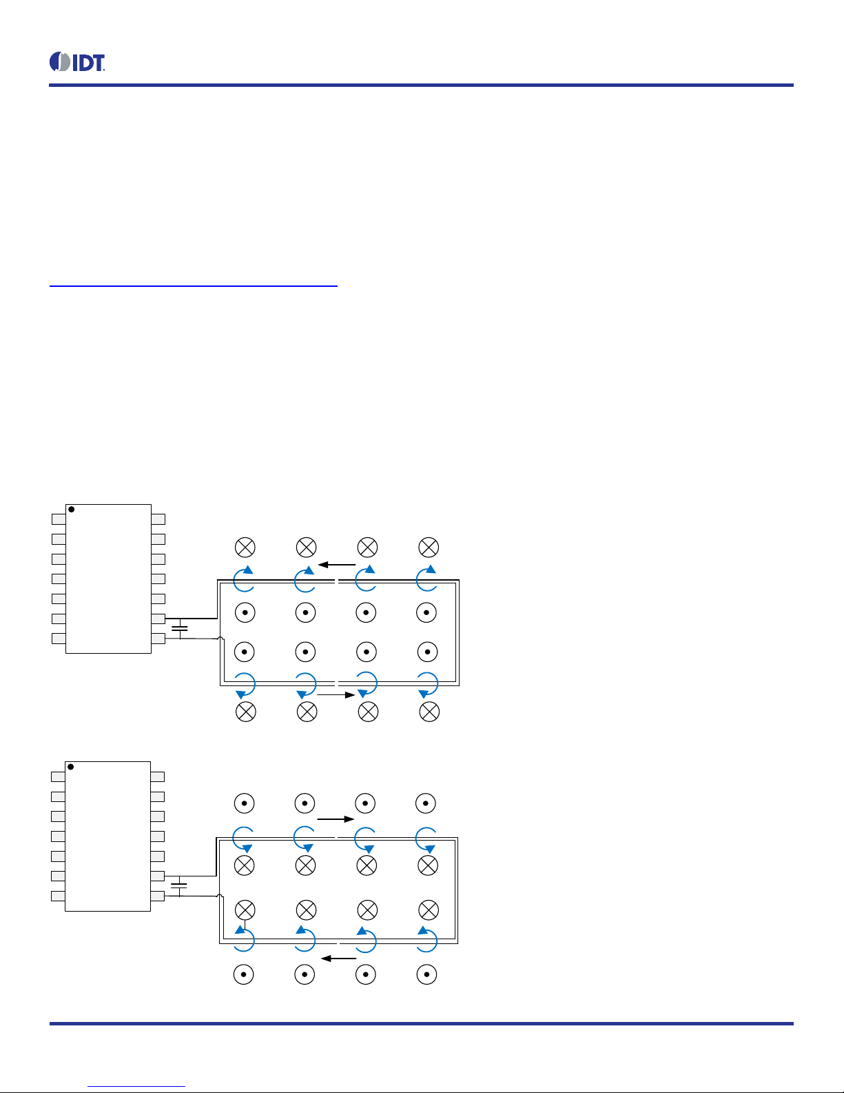
The signal that is generated by the magnetic field of transmitter coil (Tx) is received by two receiver coils.
If a metallic target is placed over the coils, the transmitted energy below the target is dissipated as eddy currents in the target and does not
induce a secondary voltage in the receiver coils in that area.
The two receiver coils are designed with a 90phase shift, and the transmitter coil surrounds them. The target is placed on top of them and
moves over a plane parallel to the plane containing all the coils, as shown in Figure 2 below. Depending on the coil’s shape, movement can be
linear, arc, or rotary. The same physical principle is valid for different coils (and target) shapes.
The position of the target will be indicated through the differential phase and the amplitude of the signals measured on the Rx coils by the
ZMID520x
Figure 2. Current Paths and Shapes for Coils –Example for Linear Position Sensing
Metallic Target
RxCos
RxSin
Tx
Sin Loop 1
(cw)
Sin Loop 2
(ccw)
Sin Loop 3
(cw)
Tx Loop
Cos Loop 2
(ccw)
Cos Loop 1
(cw)
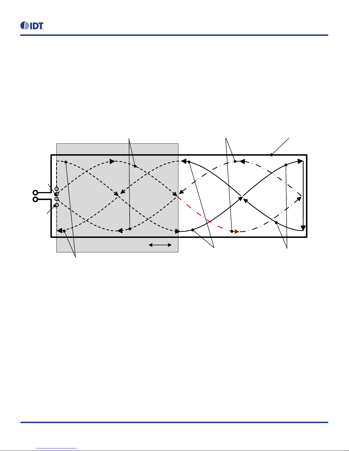
The key parameters influencing the proper operation of coils with the ZMID520x are the following: the length and width of the Tx and Rx coils,
the size of the target, and the airgap between the target and the printed circuit board (PCB) where the coils are integrated. Figure 3 provides
an illustration of the length and width of the coils for linear position sensing.

ZMID520x User Guide for Getting Started
© 2018 Integrated Device Technology, Inc.
5
April 6, 2018
Figure 3. Geometrical Illustration for Coils and Target –Example for Linear Position Sensing
Note: The following display was created by the ZMID520x Inductive Coil Design Tool Software.
IDT provides a software tool to support coil design as illustrated in Figure 3:
ZMID520x Inductive Coil Design Tool Software: https://www.idt.com/document/swr/zmid520x-inductive-coil-design-tool-software
ZMID520x User Guide –Inductive Coil Design Tool: https://www.idt.com/document/mas/zmid520x-user-guide-inductive-coil-design-tool
Reference designs for linear, arc and rotary position sensors are shown in the “Layout” section of the applicable Application Modules User
Manual available on the following application module product pages, which also provide relevant Gerber design files:
ZMID520xMLIN Application Module:
www.idt.com/products/sensor-products/position-sensors/zmid5201mlin-zmid5201-inductive-linear-application-module-analog-output
www.idt.com/products/sensor-products/position-sensors/zmid5202mlin-zmid5202-inductive-linear-application-module-pwm-output
www.idt.com/products/sensor-products/position-sensors/zmid5203mlin-zmid5203-inductive-linear-application-module-sent-output
ZMID520xMARC Application Module:
www.idt.com/products/sensor-products/position-sensors/zmid5201marc-zmid5201-inductive-arc-application-module-analog-output
www.idt.com/products/sensor-products/position-sensors/zmid5202marc-zmid5202-inductive-arc-application-module-pwm-output
www.idt.com/products/sensor-products/position-sensors/zmid5203marc-zmid5203-inductive-arc-application-module-sent-output
ZMID520xMROT Application Module:
www.idt.com/products/sensor-products/position-sensors/zmid5201mrot-zmid5201-inductive-rotary-application-module-analog-output
www.idt.com/products/sensor-products/position-sensors/zmid5202mrot-zmid5202-inductive-rotary-application-module-pwm-output
www.idt.com/products/sensor-products/position-sensors/zmid5203mrot-zmid5203-inductive-rotary-application-module-sent-output

ZMID520x User Guide for Getting Started
© 2018 Integrated Device Technology, Inc.
6
April 6, 2018
2.1 Device Block Diagram
Refer to the ZMID520x Datasheet for the latest block diagram information.
The main building blocks include the following:
Power management: power-on-reset (POR) circuit and low drop-out (LDO) regulators for internal supplies.
Oscillator: generation of the transmit coil signal.
Analog front-end: demodulator and gain control for the receive signals.
Analog-to-digital converter (ADC): conversion into digital domain.
Digital signal processing: offset correction; conversion of sine and cosine signals into angle and magnitude; angle range adjustment; and
linearization.
EEPROM: nonvolatile storage of factory and user-programmable settings.
One-wire interface (OWI): programming of the chip through the output pin.
Interface options:
Analog output for ZMID5201
PWM output for ZMID5202
SENT output for ZMID5203
Protection: overvoltage, reverse polarity, short circuit protection.
Figure 4. Main Internal Functional Block Diagram

ZMID520x User Guide for Getting Started
© 2018 Integrated Device Technology, Inc.
7
April 6, 2018
3. Getting Started
The following procedures require the ZMID520x EVK Application Software, which includes the graphical user interface (GUI) provided for the
ZMID520x Application Modules.
A complete description of the GUI is given in the ZMID520x Evaluation Kit User Manual, which is available on the IDT website via the following
link, and it includes instructions for downloading and installing the GUI: https://www.idt.com/document/man/zmid520x-evaluation-kit-user-
manual-application-modules.
3.1 LC Tank –Tx Front-End Tuning
The transmit circuitry for ZMID520x applications consists of an LC tank that is formed from the inductance of the transmitting coil and a capacitor
on the circuit board as shown in Figure 5.
Figure 5. ZMID520x Transmitter LC Tank
The objective of the Tx front-end tuning is to set the oscillation frequency in the range of operation specified in the ZMID520x Datasheet; a
typical value is approximately 3.5MHz.
The first step is to measure the inductance value of the Tx coil and verify that the value is within the limits specified in the ZMID520x Datasheet.
Once the inductor value is known, the capacitor value (Ct in Figure 5) can be calculated using Equation 1.
f = 1
2𝜋√ LC
Equation 1
Direct measurement of the frequency will confirm the exact value of the oscillation frequency.
If the measurement of the inductance of the printed circuit board coil (Lt in Figure 5) is not an option, a successive approximation approach can
be used; i.e., testing multiple Ct values until the resulting oscillation frequency is as close as possible to 3.5MHz. A capacitor value of 560pF is
generally a good starting point.
Recommendation: To ensure a good quality factor and low temperature drift for the LC tank circuit, use ceramic capacitors class C0G (C-zero-
G) ceramics also known as NP0 (negative-positive-zero). The capacitor must be placed close to the EP and EN pins on the ZMID520x.

ZMID520x User Guide for Getting Started
© 2018 Integrated Device Technology, Inc.
8
April 6, 2018
Figure 6 shows the TX pin oscillation detected with a LF-U 5 Near-Field Probe from Langer EMV-Technik.
Figure 6. TX Oscillation and LF-U 5 Probe
3.2 Device Initialization
3.2.1 Output Mode Selection
The ZMID allows selecting one of two output modes: Linear or Modulo 360.
Linear: The Linear Output Mode is a non-repeating output mode in which the sensor output signal is clamped at the mechanical end
points.
Modulo 360: The Modulo 360 Output (Sawtooth Output) Mode is a repeating output mode in which the sensor output signal is not
clamped at the mechanical end points, but it is switched back to its origin.
See the ZMID520x Datasheet and ZMID520x EVK User Manual for further details.
In most linear and arc applications, the Linear Output Mode is recommended. For rotary applications, the Modulo 360 Mode is recommended.
To ensure a smooth and successful procedure, use the GUI and the instructions in the ZMID520x EVK User Manual to set the ZMID520x
EEPROM registers from 00HEX to 09HEX to the following values. Note: Ensure that the new values are stored in EEPROM using the “Write
EEPROM” function.
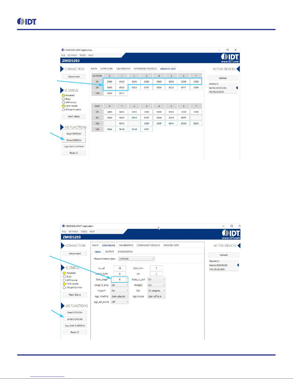
If using the Linear Output Mode, set the following register values as shown in Figure 7: register 00HEX = 2400 HEX; register 01HEX = 0400HEX;
and registers 02HEX through 09HEX = 0000HEX.
If using the Modulo 360 Output Mode, set register 00HEX = 0000HEX, register 01HEX = 0400HEX, registers 02HEX through 08HEX = 0000HEX,
and register 09HEX = 1000HEX.
ZMID520x User Guide for Getting Started
© 2018 Integrated Device Technology, Inc.
9
April 6, 2018
Figure 7. ZMID520x EEPROM Memory Values –ZMID5203 Example for the Linear Output Mode Settings
Set these standard values
for registers 00HEX to 09HEX.
Remaining register values
might differ.
Write new values to the
ZMID520x EEPROM.
3.3 Offset Check for Rx Coils
The ZMID520x has a selectable input gain, which can be set via the GUI using the Gain_stage entry field found on the “INPUT” subtab under
the “CONFIGURE” tab as described in section 3.4. Before checking the offset of the Rx coils, set the Gain_stage value to a preliminary setting
of 6 using the entry field shown in the example for the ZMID5203 given in Figure 8, which is applicable to all ZMID520x ICs.
Save the new value in the ZMID520x EEPROM memory by clicking the “Write EEPROM” button,which updates register 0CHEX.
Figure 8. ZMID520x EEPROM Gain Stage Setting –Example using the ZMID5203
Set Gain_stage to 6.
Write new values to the
ZMID520x EEPROM.
ZMID520x User Guide for Getting Started
© 2018 Integrated Device Technology, Inc.
10
April 6, 2018
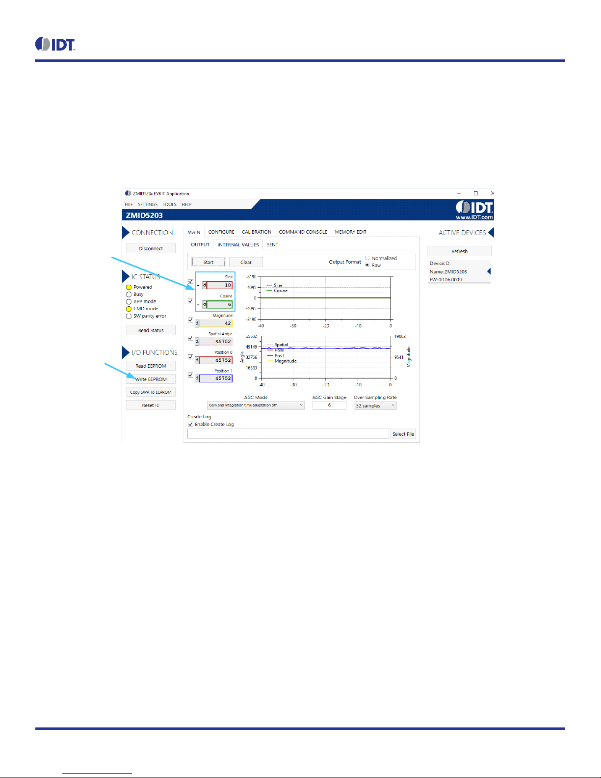
Next, remove the target from the sensor board (distance between the target and the Rx coils must be greater than 20mm). With this condition,
use the GUI to read the “Sine” and “Cosine” values on the “INTERNAL VALUES” subtab under the “MAIN” tab as shown in the ZMID5203
example given in Figure 9.
For properly designed coils, typical offset values are below 100DEC for “Sine” and “Cosine” values as shown in the example in Figure 9.
The coil design should meet the criteria of having a maximum symmetry for the two Rx coils. See section 2 for the links for software and
documentation for the ZMID520x Inductive Coil Design Tool Software provided by IDT for addressing this requirement.
Figure 9. Coil Offset Reading –Example using the ZMID5203
Check that offset values
are within requirements.
Write new values to the
ZMID520x EEPROM.

ZMID520x User Guide for Getting Started
© 2018 Integrated Device Technology, Inc.
11
April 6, 2018
3.4 Gain Stage Setting
Select the value of the Gain_stage setting so that the value of the “Magnitude” parameter is in the range of 6000DEC to 10000DEC when the
target is positioned at the nominal air gap over the sensor board. The GUI displays the “Magnitude” parameter tab on the “INTERNAL VALUES”
subtab under the “MAIN” tab for checking that this requirement has been met. In the ZMID5203 example given in Figure 10, Gain_stage has
been set to 8 DEC resulting in a “Magnitude” value within the required range.
For most applications, the automatic gain control (ACG) functionality can be disabled (see the “AGC Mode” setting in Figure 10).
Figure 10. Magnitude for Gain Selection –Example for the ZMID5203
ZMID520x User Guide for Getting Started
© 2018 Integrated Device Technology, Inc.
12
April 6, 2018
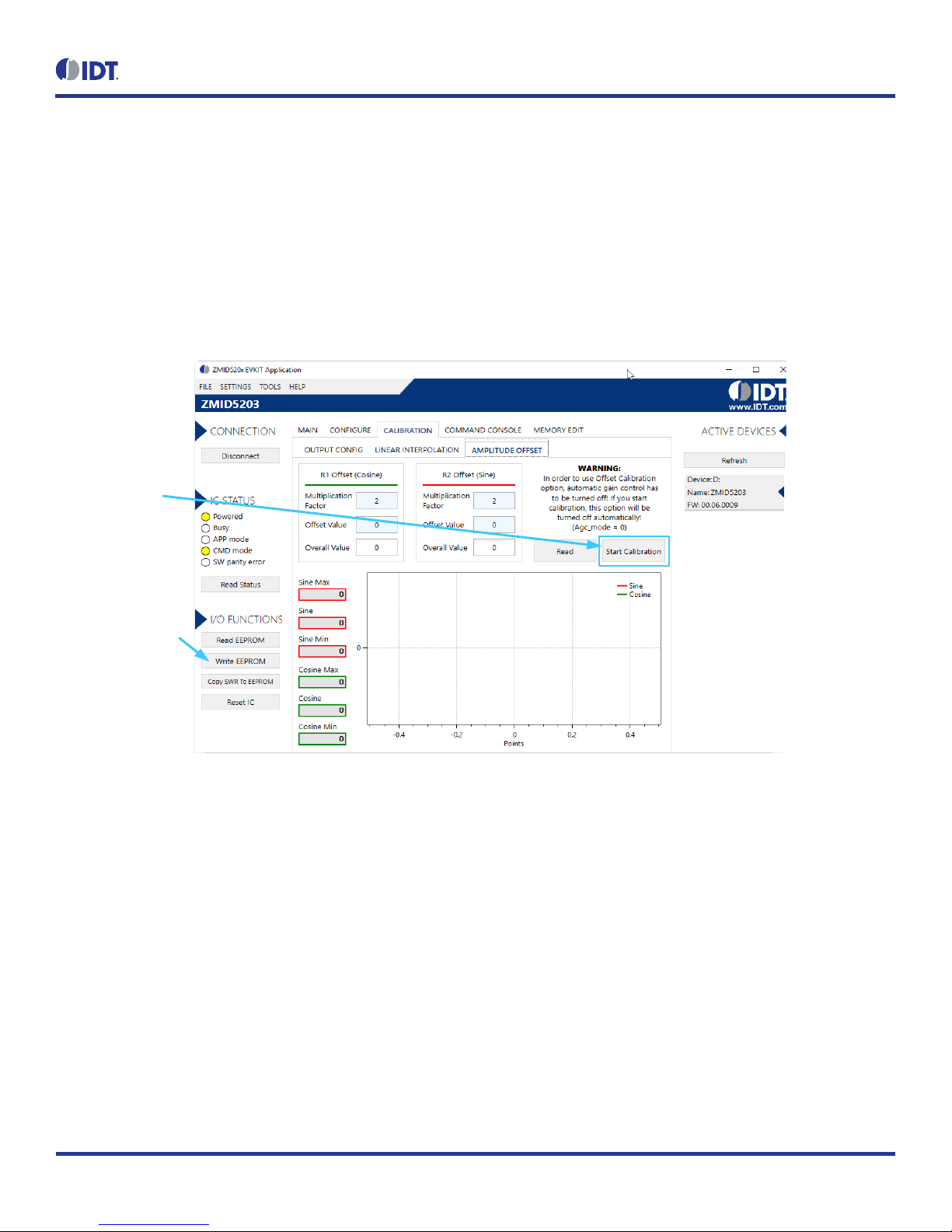
3.5 Input Amplitude Offset Compensation
The GUI offers an automated procedure for performing the input amplitude offset compensation with the target in place. For this procedure the
target must be positioned at the operational distance from the receiving coils (air gap).
1. Start the procedure by clicking the “Start Calibration” button located on the “AMPLITUDE OFFSET” subtab under the “CALIBRATION” tab
as shown in the ZMID5203 example given in Figure 11, which applies to all ZMID520x ICs. Follow instructions in the resulting dialog
windows to complete the calibration.
2. When the calibration is finished, click the “Write to EEPROM” button before moving to the next steps. This procedure modifies the contents
of register 08HEX.
Figure 11. ZMID520x Input Amplitude Offset Compensation –Example for the ZMID5203
Click here to start the
automatic calibration.
When the automatic
calibration is completed,
write the new values to
the ZMID520x EEPROM.
ZMID520x User Guide for Getting Started
© 2018 Integrated Device Technology, Inc.
13
April 6, 2018
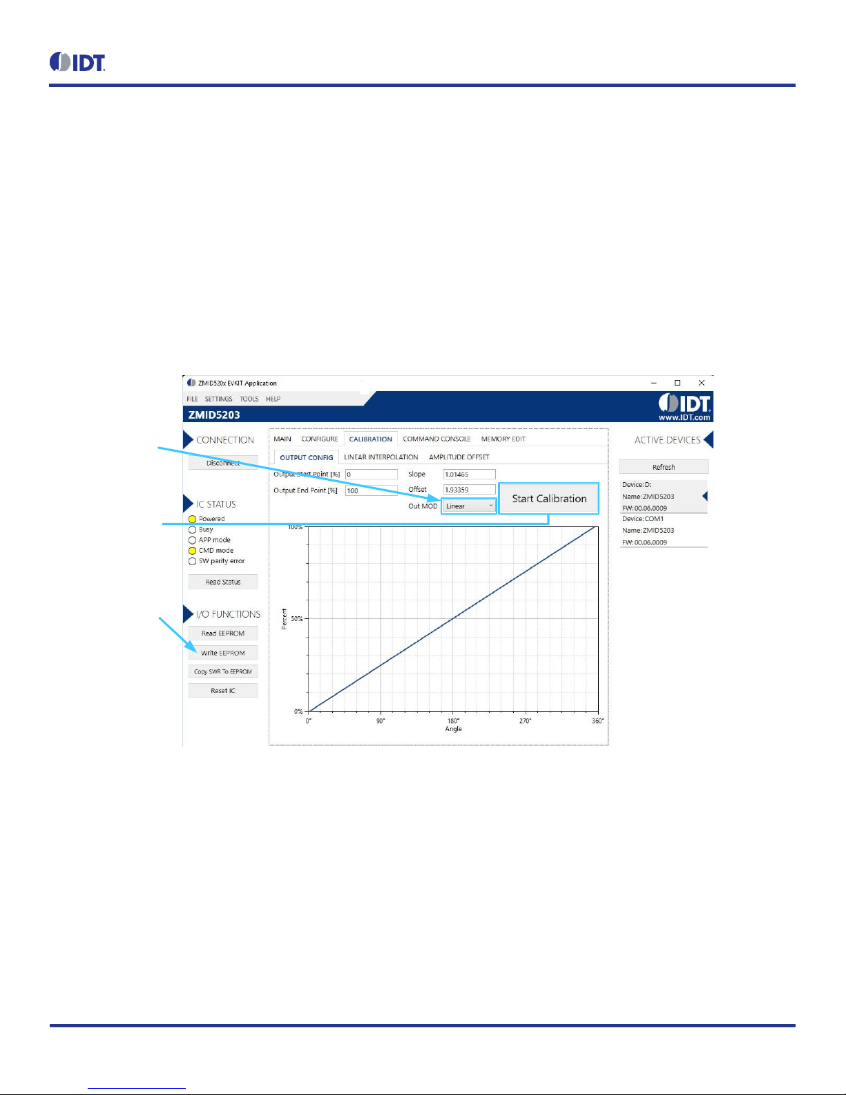
3.6 Output Calibration
The GUI offers an automated procedure for performing output calibration with the target in place at the operational distance from the receiving
coils (air gap).
1. Select the “Out MODE” setting as described in section 3.2.1.
2. Start the procedure by clicking the “Start Calibration” button on the “OUTPUT CONFIG” subtab under the “CALIBRATION” tab as shown
in the ZMID5203 example given in Figure 12.
3. Click the “Write to EEPROM” button before moving to the next steps. This procedure modifies the contents of registers 00HEX, 01HEX, and
09HEX.
4. Verify that the calibration was successful by checking the “Position 1”field on the “INTERNAL VALUES” subtab under the “MAIN” tab at
the start and end positions of the measurement range via the “INTERNAL VALUES” subtab under the “MAIN” tab as shown in the ZMID5203
example given in Figure 13, which applies to all ZMID520x ICs.
Figure 12. Output Calibration
Then click here to start
the automatic calibration.
When the automatic
calibration is completed,
write the new values to
the ZMID520x EEPROM.
Select the output mode:
Linearfor arc and
linear applications
Modulus 360for
rotary applications

ZMID520x User Guide for Getting Started
© 2018 Integrated Device Technology, Inc.
14
April 6, 2018
Figure 13. Output Calibration Verification
End point = ~65535
Click Startand then
move target.
Start point = 0
3.7 Output Linearization
This section provides a basic output linearization procedure for the ZMID520x. Using a target positioning system for these procedures is strongly
recommended.
For additional information on calibration and linearization, refer to the ZMID520x Evaluation Kit User Manual. For the ZMID5201, also see the
ZMID5201 Manual for Calibration and Linearization Using the Analog Output available on the ZMID5201 product web page.
www.idt.com/document/man/zmid5201-manual-calibration-and-linearization-using-analog-output
1. Set the “Correction Mode" drop-down menu to “Post-calibration” on the “LINEAR INTERPOLATION” subtab under the “CALIBRATION”
tab (see Figure 14). This modifies register 09HEX.
2. Set the value for the “Motion Range” entry field according to the receiver coil shape.
Figure 14. Correction Mode Selection
Set Correction Mode
to Post-calibration.
Set Motion Rangevalue
according to the application.

ZMID520x User Guide for Getting Started
© 2018 Integrated Device Technology, Inc.
15
April 6, 2018
3. Select the “Raw” mode via the radio buttons above the fields for “Spatial Angle,” “Position 0,”and “Position 1” as shown in Figure 15.
4. Click the “Start Reading” button to start reading position values via the ZMID520x. The button changes to “Stop,” and the adjacent readings
should update to show the position readings.
5. Move the actual target position until the value in the “Position 0” field is 0000HEX. Note: The points identified by “Position 0” = 0000HEX and
“Position 0” = FFFFHEX are the start and end points identified with the calibration procedure.
6. Then physically measure the actual position or read the measured value from the positioning system (in mm or degrees) and enter the
value in the first column in the “Measured Value” row in the matrix on the “LINEAR INTERPOLATION” tab. Figure 15 shows an example
of the matrix for a 360 rotary position sensing application for the ZMID5203.
Figure 15. Measured Value Readings for 9 Linearization Points
Enter the physical
measurement in mm
or degrees; e.g. from
the positioning system.
Click Start Reading
to start reading the
measured values
from the ZMID520x.
Select RawMode.
7. Move the target again (e.g., with the positioning system) until the value in the “Position 0” field is 1FFFHEX. Then physically measure the
new actual position or read the measured value from the positioning system and enter the value in the second column in the “Measured
Value” row in the matrix.
8. Repeat the previous step for “Position 0” = (1FFF x n) + n –1 where n = 2 to 8 to obtain actual measurements for the remaining positions
in the matrix so that all 9 linearization points identified in Figure 16 have measured values entered in the “Measured Value” row.
The software immediately calculates the correction values, and the resulting values are displayed below the applicable “Measured Values”
entry.
9. Click on “Write EEPROM” to save the new values in registers 03HEX to 07HEX.
The linearization procedure is completed. The values in the Pos1 register will differ from those in Pos0 register, reflecting the linearization
correction performed (see Table 1). The device is ready for operation in the application environment.

ZMID520x User Guide for Getting Started
© 2018 Integrated Device Technology, Inc.
16
April 6, 2018
Figure 16. Input Fields for the 9 Linearization Points Measured Values
Advance the target and
enter actual measured
position values (e.g.,
from the positioning
system) in each column.
Click here to stop
reading measured
values.

ZMID520x User Guide for Getting Started
© 2018 Integrated Device Technology, Inc.
17
April 6, 2018
4. Internal Memory
Figure 17 shows the internal memory structure of the ZMID520x products, which is divided into a nonvolatile EEPROM and a volatile shadow
RAM (SWR) section. After the ZMID520x start up, the EEPROM content is copied into the SWR. During ZMID520x operation in OWI mode,
changes in the SWR will take immediate effect; whereas changes in the EEPROM require a memory WRITE command or a ZMID520x power
cycle (power off / power on).
Figure 17. ZMID520x Internal Memory
Memory
EEPROM Shadow Register
(SWR)
Communication IF
One Wire Interface (OWI)
1FHEX
00HEX
1FHEX
00HEX
PPU
Output
Traceability
Others
Table 1. EEPROM and Shadow RAM Contents
Address
Type
Location
Function
00HEX
R/W
EEPROM/SWR
This register value is the 14-bit zero-angle offset of output signal, which is used for device
calibration and sets the offset value of the output transfer function.
01HEX
R/W
EEPROM/SWR
This register value is the 13-bit slope value of output signal, which is used for device
calibration and sets the slope value of the output transfer function.
02HEX
R/W
EEPROM/SWR
This register value is used with the analog and PWM output protocols in order to clamp the
upper and lower output levels of the transfer function respectively below 95% and above 5%.
03HEX
R/W
EEPROM/SWR
This register value is used in linearization. The position transfer function can be modified by a
correction curve over the whole position range. The correction curve is defined by 9
linearization points. This register contains the correction factor for points n°2 and n°1. Bits
[15:8] are the correction factor for the position at 12.5% (45°), and bits [7:0] are the correction
factor for the position at 0% (0°).
04HEX
R/W
EEPROM/SWR
This register value is used in linearization (see register 03HEX for description). This register
contains the correction factor for points n°4 and n°3.
Bits [15:8] are the correction factor for the position at 37.5% (135°), and bits [7:0] are the
correction factor for the position at 25% (90°).

ZMID520x User Guide for Getting Started
© 2018 Integrated Device Technology, Inc.
18
April 6, 2018
Address
Type
Location
Function
05HEX
R/W
EEPROM/SWR
This register value is used in linearization (see register 03HEXfor description). This register
contains the correction factor for points n°6 and n°5.
Bits [15:8] are the correction factor for the position at 62.5% (225°), and bits [7:0] are the
correction factor for the position at 50% (180°).
06HEX
R/W
EEPROM/SWR
This register value is used in linearization (see register 03HEXfor description). This register
contains the correction factor for points n°8 and n°7.
Bits [15:8] are the correction factor for the position at 87.5% (315°), and bits [7:0] are the
correction factor for the position at 75% (270°).
07HEX
R/W
EEPROM/SWR
This register value is used in linearization (see register 03HEXfor description). This register
contains the correction factor for point n°9.
Bits [15:8] are not used, and bits [7:0] are the correction factor for the position at 100% (360°).
08HEX
R/W
EEPROM/SWR
This register value is the signal offset correction of the demodulated input signals sin and cos
(R1and R2). It is used for input amplitude offset correction; the defined register offset values
are added/subtracted to/from the amplitude values of the receiver coil values.
09HEX
R/W
EEPROM/SWR
This register contains the control bits for selecting the output mode of the sensor (Linear
Output Mode or Modulo 360 Output Mode), the type of linearization (pre or post-calibration),
the angle offset for linearity correction (0° or -22.5°), the option to reverse the polarity of the
receiver coils, and the option to invert the phase polarity of the receiver coils.
0AHEX
R/W
EEPROM/SWR
This register value is used to define the type of communication interface (SENT, analog, or
PWM). It is used for configuration of the output SENT CRC, SENT pause; PWM slope current,
PWM frequency, and analog diagnostic level.
0BHEX
R/W
EEPROM/SWR
This register value is used to control the voltage of the internal VDDT voltage regulator, the
current of the Tx excitation coil, the oversampling rate of the ADC, and the PWM output slope
time.
0CHEX
R/W
EEPROM/SWR
This register value is used to set the gain stage value, the adjustment of the integration cycle
in relation to the Tx coil period, and the integration time in terms of the ADC sample periods
vs. the oversampling rate.
0DHEX
R/W
EEPROM/SWR
This register value is used to set the CORDIC magnitude upper and lower levels, the upper
and lower limits for the Tx coil frequency, the gain and integration time adaptation combined
settings, and mixed operation modes.
0EHEX
R/W
EEPROM/SWR
This register value is used to mask diagnostic register bits to prevent a diagnostic flag setting
the output in the diagnostic status.
0FHEX
R/W
EEPROM
Internal use only.
10HEX
R/W
EEPROM
Internal use only.
11HEX
R/W
EEPROM/SWR
This register value is used to the trigger actions for the shadow register, diagnostic register, Tx
coil alarm, Rx coils alarm, double-error detection for the EEPROM memory, parity error
detection on the SWR memory, ADC overflow, AGC offset saturation, Tx coil alarm, and a set
of parameters used in test mode only.
13HEX
R
SWR
This register value is used for analog front-end / automatic gain regulation; polarity of R1 and
R2 ADC gain; and number of integration cycles for the AGC.
14HEX
R
SWR
This register value is the 13-bit CORDIC raw input signal for Xsine.
15HEX
R
SWR
This register value is the 13-bit CORDIC raw input signal for Ycosine.
16HEX
R
SWR
This register value is the 15-bit CORDIC output angle (0° to 90°).

ZMID520x User Guide for Getting Started
© 2018 Integrated Device Technology, Inc.
19
April 6, 2018
Address
Type
Location
Function
17HEX
R
SWR
This register value is the 15-bit CORDIC output magnitude.
18HEX
R
SWR
This register value is the 16-bit output spatial angle (0° to 360°) before output calibration and
linear error correction.
19HEX
R
SWR
This register value is Position 0, which is the 16-bit output angle (0° to 360°) after output
calibration. If linearization is done before the output calibration, this value = Position 1. If
linearization is done after the output calibration, this value is not the same value as Position 1.
1AHEX
R
SWR
This register value is Position 1, which is the 16-bit output angle (0° to 360°) after output
calibration and linearization. This value is always affected by linearization.
1BHEX
R
SWR
Internal use only.
Complete information about registers map is available upon request. Contact: https://www.idt.com/support
5. Programming the ZMID520x EEPROM
The ZMID520x EEPROM can be programmed using the ZMID-COMBOARD USB Communication and Programming Board for ZMID Application
Modules in conjunction with the ZMID520x EVK Application Software. Instructions for using the software to program the EEPROM are given in
the ZMID520x Evaluation Kit User Manual. See section 2.1 for details for obtaining the software and the kit manual.
Additional information and documentation for the ZMID-COMBOARD are provided on the following IDT web page:
https://www.idt.com/products/sensor-products/position-sensors/zmid-comboard-usb-communication-and-programming-board-zmid-
application-modules
6. Glossary
Acronym
Definition
ADC
Analog Digital Converter
AGC
Automatic Gain Control
EEPROM
Electrically Erasable Programmable Read Only Memory
LSB
Least Significant Bit
MSB
Most Significant Bit
OWI
One-Wire Interface
OSR
Over-Sampling Rate
SWR
Shadow Word Register Bank

ZMID520x User Guide for Getting Started
© 2018 Integrated Device Technology, Inc.
20
April 6, 2018
7. Revision History
Revision Date
Description of Change
April 6, 2018
Initial release
Corporate Headquarters
6024 Silver Creek Valley Road
San Jose, CA 95138
www.IDT.com
Sales
1-800-345-7015 or 408-284-8200
Fax: 408-284-2775
www.IDT.com/go/sales
Tech Support
www.IDT.com/go/support
DISCLAIMER Integrated Device Technology, Inc. (IDT) and its affiliated companies (herein referred to as “IDT”) reserve the right to modify the products and/or specificatio ns described herein at any time,
without notice, at IDT's sole discretion. Performance specifications and operating parameters of the described products are determined in an independent state and are not guaranteed to perform the same
way when installed in customer products. The information contained herein is provided without representation or warranty of a ny kind, whether express or implied, including, but not limited to, the suitability
of IDT's products for any particular purpose, an implied warranty of merchantability, or non-infringement of the intellectual property rights of others. This document is presented only as a guide and does not
convey any license under intellectual property rights of IDT or any third parties.
IDT's products are not intended for use in applications involving extreme environmental conditions or in life support systems or similar devices where the failure or malfunction of an IDT product can be
reasonably expected to significantly affect the health or safety of users. Anyone using an IDT product in such a manner does so at their own risk, absent an express, written agreement by IDT.
Integrated Device Technology, IDT and the IDT logo are trademarks or registered trademarks of IDT and its subsidiaries in the United States and oth er countries. Other trademarks used herein are the
property of IDT or their respective third party owners. For datasheet type definitions and a glossary of common terms, visit www.idt.com/go/glossary. All contents of this document are copyright of Integrated
Device Technology, Inc. All rights reserved.
This manual suits for next models
2
Table of contents
Other IDT Accessories manuals


