Infineon TRAVEO T2G family CYT4D Series User manual

Application Note Please read the Important Notice and Warnings at the end of this document 002-26071 Rev. *B
www.infineon.com page 1 of 80 2021-09-07
AN226071
Clock configuration setup in TRAVEO™ T2G
family CYT4D series MCUs
About this document
Scope and purpose
AN226071 describes how to set up the various clock sources in TRAVEO™ T2G family CYT4D series MCUs and
provides examples including configuring PLL/FLL and calibrating the ILO.
Associated part family
TRAVEO™ T2G family CYT4D series automotive microcontrollers
Intended audience
This document is intended for users who use the clock configuration setup in TRAVEO™ T2G family CYT4D series
MCUs.
Table of contents
About this document......................................................................................................................... 1
Table of contents .............................................................................................................................. 1
1Introduction ............................................................................................................................ 3
2Clock system for TRAVEO™ T2G family MCUs............................................................................... 4
2.1 Overview of the clock system .................................................................................................................4
2.2 Clock resources .......................................................................................................................................4
2.3 Clock system functions ...........................................................................................................................4
2.4 Basic clock system settings...................................................................................................................11
3Configuration of the clock resources.........................................................................................12
3.1 Setting the ECO .....................................................................................................................................12
3.1.1 Use case............................................................................................................................................13
3.1.2 Configuration ...................................................................................................................................13
3.1.3 Sample code for initial ECO configuration......................................................................................14
3.2 Setting WCO...........................................................................................................................................20
3.2.1 Operation overview..........................................................................................................................20
3.2.2 Configuration ...................................................................................................................................20
3.2.3 Sample code for the initial configuration of WCO settings ............................................................21
3.3 Configuring IMO.....................................................................................................................................22
3.4 Configuring ILO0/ILO1...........................................................................................................................22
3.5 Setting the LPECO .................................................................................................................................23
3.5.1 Use case............................................................................................................................................23
3.5.2 Sample code for the initial configuration of LPECO settings .........................................................24
4Configuration of the FLL and PLL ..............................................................................................26
4.1 Setting FLL.............................................................................................................................................26
4.1.1 Operation overview..........................................................................................................................26

Application Note 2 of 80 002-26071 Rev. *B
2021-09-07
Clock configuration setup in TRAVEO™ T2G family CYT4D series MCUs
Table of contents
4.1.2 Use case............................................................................................................................................27
4.1.3 Configuration ...................................................................................................................................27
4.1.4 Sample code for the initial configuration of FLL settings...............................................................28
4.2 Setting PLL.............................................................................................................................................31
4.2.1 Use case............................................................................................................................................33
4.2.2 Configuration ...................................................................................................................................33
4.2.3 Sample code for the initial PLL configuration ................................................................................39
5Configuring the internal clock ..................................................................................................48
5.1 Configuring CLK_PATHx........................................................................................................................48
5.2 Configuring CLK_HFx ............................................................................................................................50
5.3 Configuring the CLK_LF.........................................................................................................................51
5.4 Configuring CLK_FAST_0/CLK_FAST_1 ................................................................................................51
5.5 Configuring CLK_MEM...........................................................................................................................51
5.6 Configuring CLK_PERI ...........................................................................................................................51
5.7 Configuring CLK_SLOW.........................................................................................................................52
5.8 Configuring CLK_GR..............................................................................................................................52
5.9 Configuring PCLK ..................................................................................................................................53
5.9.1 Example of PCLK setting ..................................................................................................................54
5.9.1.1 Use case.......................................................................................................................................54
5.9.1.2 Configuration ..............................................................................................................................54
5.9.2 Sample code for the initial configuration of PCLK settings (example of the TCPWM timer).........55
5.10 Setting ECO_Prescaler ..........................................................................................................................57
5.10.1 Use case............................................................................................................................................58
5.10.2 Configuration ...................................................................................................................................58
5.10.3 Sample code for the initial configuration of ECO prescaler settings .............................................59
5.11 Configuring the LPECO_Prescaler ........................................................................................................61
5.11.1 Use case............................................................................................................................................61
5.11.2 Configuration ...................................................................................................................................62
5.11.3 Sample code for the initial configuration of LPECO prescaler settings .........................................62
6Supplementary information.....................................................................................................65
6.1 Input clocks in peripheral functions.....................................................................................................65
6.2 Use case of the clock calibration counter function..............................................................................66
6.2.1.1 Use case.......................................................................................................................................67
6.2.1.2 Configuration ..............................................................................................................................67
6.2.1.3 Sample code for the initial configuration of the clock calibration counter with ILO0 and ECO
settings ........................................................................................................................................68
6.2.2 ILO0 calibration using the clock calibration counter function.......................................................70
6.2.2.1 Configuration ..............................................................................................................................71
6.2.2.2 Sample code for the initial configuration of ILO0 calibration using clock calibration counter
settings ........................................................................................................................................71
6.3 CSV diagram and relationship of the monitored clock and reference clocks.....................................73
7Glossary .................................................................................................................................75
References ......................................................................................................................................77
Other references..............................................................................................................................78
Revision history...............................................................................................................................79

Application Note 3 of 80 002-26071 Rev. *B
2021-09-07
Clock configuration setup in TRAVEO™ T2G family CYT4D series MCUs
Introduction
1Introduction
TRAVEO™ T2G family MCUs, targeted at automotive systems such as instrument clusters and head-up display
(HUD), have a 2D graphics engine, sound processing, 32-bit automotive microcontrollers based on the Arm®
Cortex®-M7 processor with FPU (single and dual precision), and manufactured on an advanced 40-nm process
technology. These products enable a secure computing platform, and incorporate Infineon low-power flash
memory along with multiple high-performance analog and digital functions.
The TRAVEO™ T2G clock system supports high-, and low-speed clocks using both internal and external clock
sources. One of the typical use case for clock input is internal real-time clock (RTC). The TRAVEO™ T2G MCU
supports phase-locked loop (PLL) and frequency-locked loop (FLL) to generate clocks that operate the internal
circuit at a high speed.
The TRAVEO™ T2G MCU also supports the function to monitor clock operation and to measure the clock
difference of each clock with reference to a known clock.
To know more on the functionality described and terminology used in this application note, see the “Clocking
system”chapter in the architecture technical reference manual (TRM).
In this document, TRAVEO™ T2G family MCUs refer to CYT4D series.
Application Note 4 of 80 002-26071 Rev. *B
2021-09-07
Clock configuration setup in TRAVEO™ T2G family CYT4D series MCUs
Clock system for TRAVEO™ T2G family MCUs
2Clock system for TRAVEO™ T2G family MCUs
2.1 Overview of the clock system
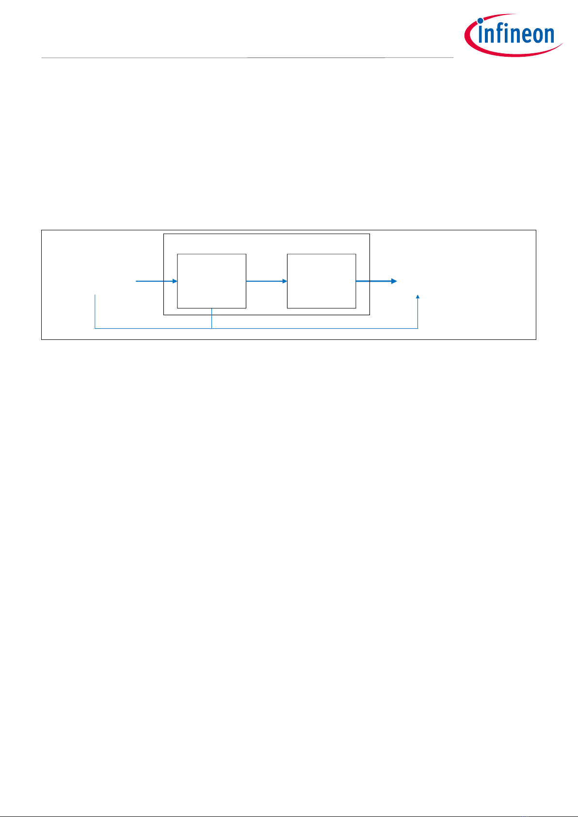
The clock system in this series of MCUs is divided into two blocks. One block selects the clock resources (such
as external oscillation and internal oscillation) and multiplies the clock (using FLL and PLL). The other block
distributes and divides clocks to the CPU cores and other peripheral functions. However, there are some
exceptions where the RTC can connect directly to a clock resource.
Figure 1 shows the overview of the clock system structure.
Clock distribution/
division
Clock selection
and multiplier
Internal circuit
(CPU core, peripheral functions,
etc.)
Clock sources
(External, Internal)
Clock system
Figure 1 Overview of the clock system structure
2.2 Clock resources
The MCUs support two types of resource inputs: internal and external. Each of these internally support three
types of clocks respectively.
•Internal clock sources (All these clocks are enabled by default):
−Internal main oscillator (IMO): This is a built-in clock with a frequency of 8 MHz (TYP).
−Internal low-speed oscillator 0 (ILO0): This is a built-in clock with a frequency of 32 kHz (TYP).
−Internal low-speed oscillator 1 (ILO1): ILO1 has the same function as ILO0, but ILO1 can monitor the clock
of ILO0.
•External clock sources (All these clocks are disabled by default):
−External crystal oscillator (ECO): This clock uses an external oscillator whose input frequency range is
between 3.988 MHz and 33.34 MHz.
−Watch crystal oscillator (WCO): This also uses an external oscillator whose frequency is stable at 32.768
kHz, mainly used by the RTC module.
−External clock (EXT_CLK): The EXT_CLK is a 0.25 MHz to 100 MHz range clock that can be sourced from a
signal on a designed I/O pin. This clock can be used as the source clock for either PLL or FLL, or can be
used directly by the high-frequency clocks.
−Low-power external crystal oscillator (LPECO): This clock uses an external oscillator. The input frequency
range is between 4 MHz and 8 MHz. The LPECO can be regarded as an ECO operating in low-power mode.
For more details on functions such as IMO, PLL, and so on, and numerical values such as frequency, see the
TRAVEO™ T2G architecture TRM and the datasheet.
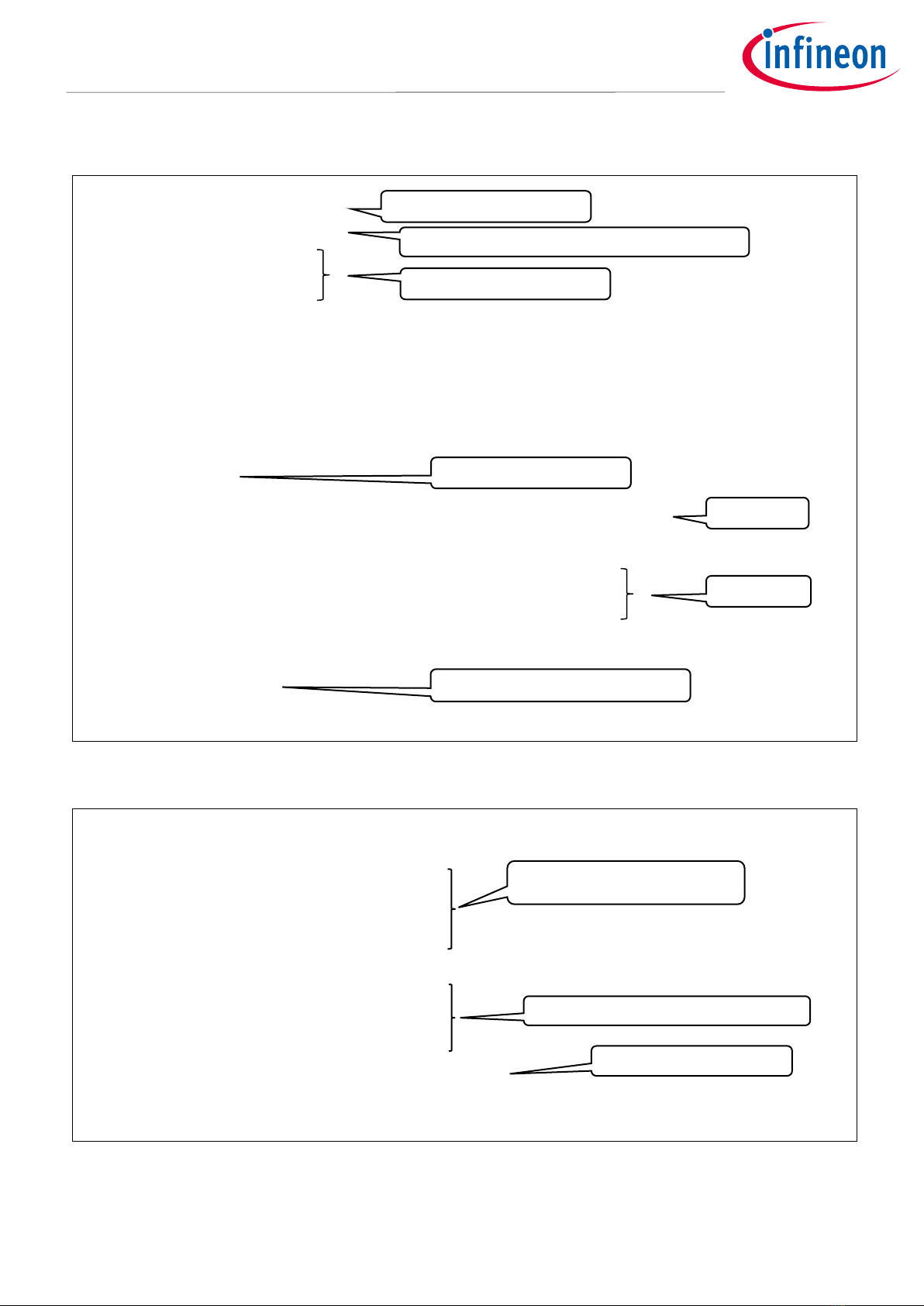
2.3 Clock system functions
Figure 2 shows the details of the clock selection and multiplier block. This block generates root frequency
clocks CLK_HF0 to CLK_HF13 from the clock resources. This block has a capability to select one of the

Application Note 5 of 80 002-26071 Rev. *B
2021-09-07
Clock configuration setup in TRAVEO™ T2G family CYT4D series MCUs
Clock system for TRAVEO™ T2G family MCUs
supported clock resources, FLL, and PLL to generate the required high-speed clocks. These MCUs support two
types of PLLs: PLL without spread spectrum clock generation (SSCG) and fractional operation (PLL200#x), and
PLL with SSCG and fractional operation (PLL400#x).
PATH_MUX4
DSI_MUX4
IMO
EXT_CLK
Predivider
(1/2/4/8)
CSV
CLK_HF1
CLK_PATH0
FLL
CLK_PATH5
PLL400
#4
CLK_PATH6
PLL200
#0
CLK_PATH7
PLL200
#1
CLK_PATH8
PLL200
#2
Predivider
(1/2/4/8)
CSV
CLK_HF2
Predivider
(1/2/4/8)
CSV
CLK_HF3
Predivider
(1/2/4/8)
CSV
CLK_HF4
Predivider
(1/2/4/8)
CSV
CLK_HF5
Predivider
(1/2/4/8)
CSV
CLK_HF6
Predivider
(1/2/4/8)
CSV
CLK_HF7
Predivider
(1/2/4/8)
CSV
CLK_HF8
CLK_PATH9
ECO
Prescaler
ECO
ILO0
ILO1
WCO
CSV
CLK_REF_HF
CSV
CSV
CLK_LF
Active Domain
DeepSleep Domain
Hibernate Domain
REF_MUX
PATH_MUX9
DSI_MUX9
ROOT_MUX5
ROOT_MUX6
ROOT_MUX7
ROOT_MUX8
ROOT_MUX4
ROOT_MUX3
ROOT_MUX2
ROOT_MUX1
PATH_MUX8
DSI_MUX8
BYPASS_MUX8
PATH_MUX7
DSI_MUX7
BYPASS_MUX7
PATH_MUX6
DSI_MUX6
BYPASS_MUX6
PATH_MUX5
DSI_MUX5
BYPASS_MUX5
BYPASS_MUX0
LFCLK_SEL
CLK_SEL
CLK_ILO0
CLK_BAK
LPECO LPECO
Prescaler
Predivider
(1/2/4/8)
CSV
CLK_HF0
ROOT_MUX0
Predivider
(1/2/4/8)
CSV
CLK_HF9
Predivider
(1/2/4/8)
CSV
CLK_HF10
Predivider
(1/2/4/8)
CSV
CLK_HF11
Predivider
(1/2/4/8)
CSV
CLK_HF12
Predivider
(1/2/4/8)
CSV
CLK_HF13
ROOT_MUX10
ROOT_MUX11
ROOT_MUX12
ROOT_MUX13
ROOT_MUX9
CLK_PATH1
PLL400
#0
CLK_PATH2
PLL400
#1
CLK_PATH3
PLL400
#2
CLK_PATH4
PLL400
#3 BYPASS_MUX4
PATH_MUX3
DSI_MUX3
BYPASS_MUX3
PATH_MUX2
DSI_MUX2
BYPASS_MUX2
PATH_MUX1
DSI_MUX1
BYPASS_MUX1
PATH_MUX0
DSI_MUX0
Figure 2 Block diagram

Application Note 6 of 80 002-26071 Rev. *B
2021-09-07
Clock configuration setup in TRAVEO™ T2G family CYT4D series MCUs
Clock system for TRAVEO™ T2G family MCUs
Active domain
Region of operation in only Active power mode
DeepSleep domain
Region of operation in only Active and DeepSleep modes
Hibernate domain
Region of operation in all power modes
ECO prescaler
Divides the ECO and creates a clock that can be used with the CLK_LF clock.
The division function has a 10-bit integer divider and 8-bit fractional divider.
LPECO prescaler
Divides the LPECO and creates a clock that can be used with the CLK_BAK. The
division function has a 10-bit integer divider and 8-bit fractional divider.
DSI_MUX
Selects a clock from ILO0, ILO1, and WCO
PATH_MUX
Selects a clock from IMO, ECO, EXT_CLK, LPECO, and DSI_MUX output
CLK_PATH
CLK_PATHx 0 through 9 are used as the input sources for high-frequency
clocks.
CLK_HF
CLK_HFx 0 through 13 are recognized as high-frequency clocks.
FLL
Generates the high-frequency clock
PLL
Generates the high-frequency clock. There are two kinds of PLL: PLL200 and
PLL400. PLL200 is with SSCG and fractional operation and PLL400 is with SSCG
and fractional operation.
BYPASS_MUX
Selects the clock to be output to the CLK_PATH. In the case of FLL, the clock
that can be selected is either FLL output or clock input to FLL.
ROOT_MUX
Selects the clock source of the CLK_HFx. The clocks that can be selected are
CLK_PATHs 0 through 9.
Predivider
The predivider (divided by 1, 2, 4, or 8) is available to divide the selected
CLK_PATH.
REF_MUX
Selects the CLK_REF_HF clock source
CLK_REF_HF
Used to monitor the CSV of the CLK_HF
LFCLK_SEL
Selects the CLK_LF clock source
CLK_LF
MCWDT source clock
CLK_SEL
Selects the clock to be input to the RTC
CLK_BAK
Mainly input to the RTC
CSV
Clock supervision to monitor the clock operation

Application Note 7 of 80 002-26071 Rev. *B
2021-09-07
Clock configuration setup in TRAVEO™ T2G family CYT4D series MCUs
Clock system for TRAVEO™ T2G family MCUs
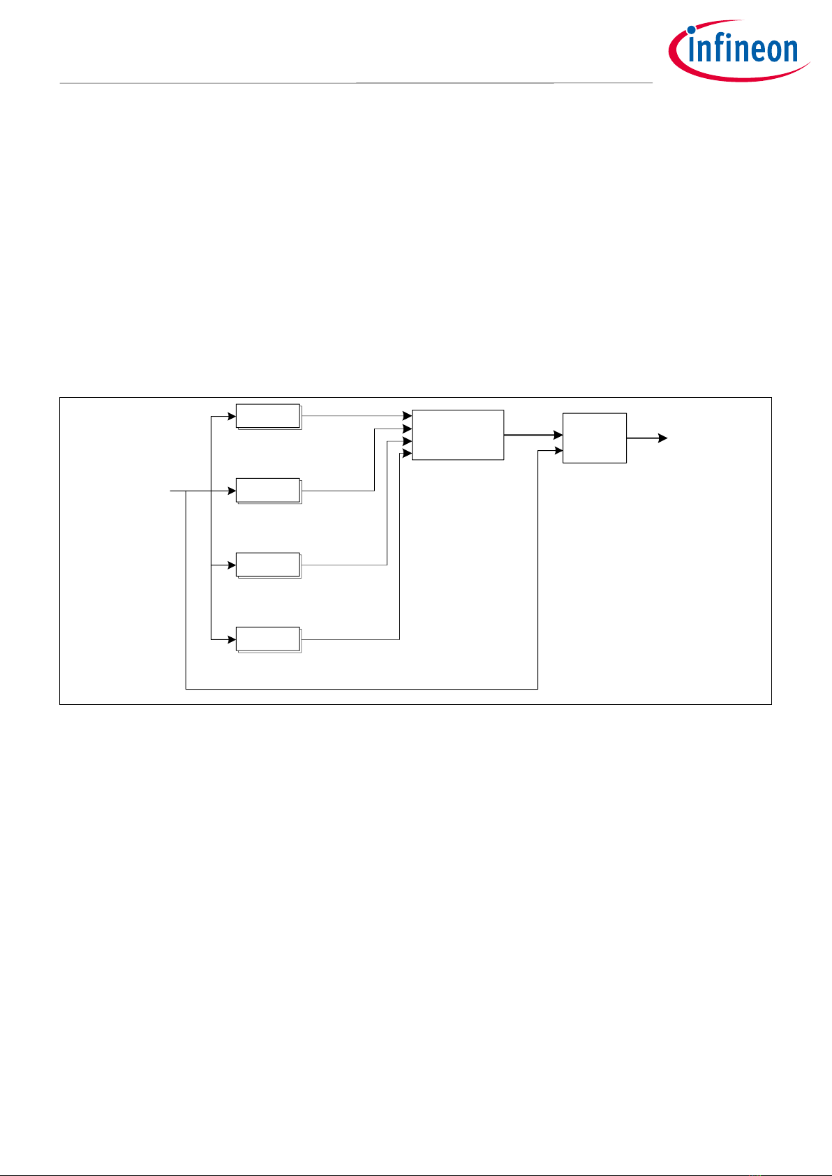
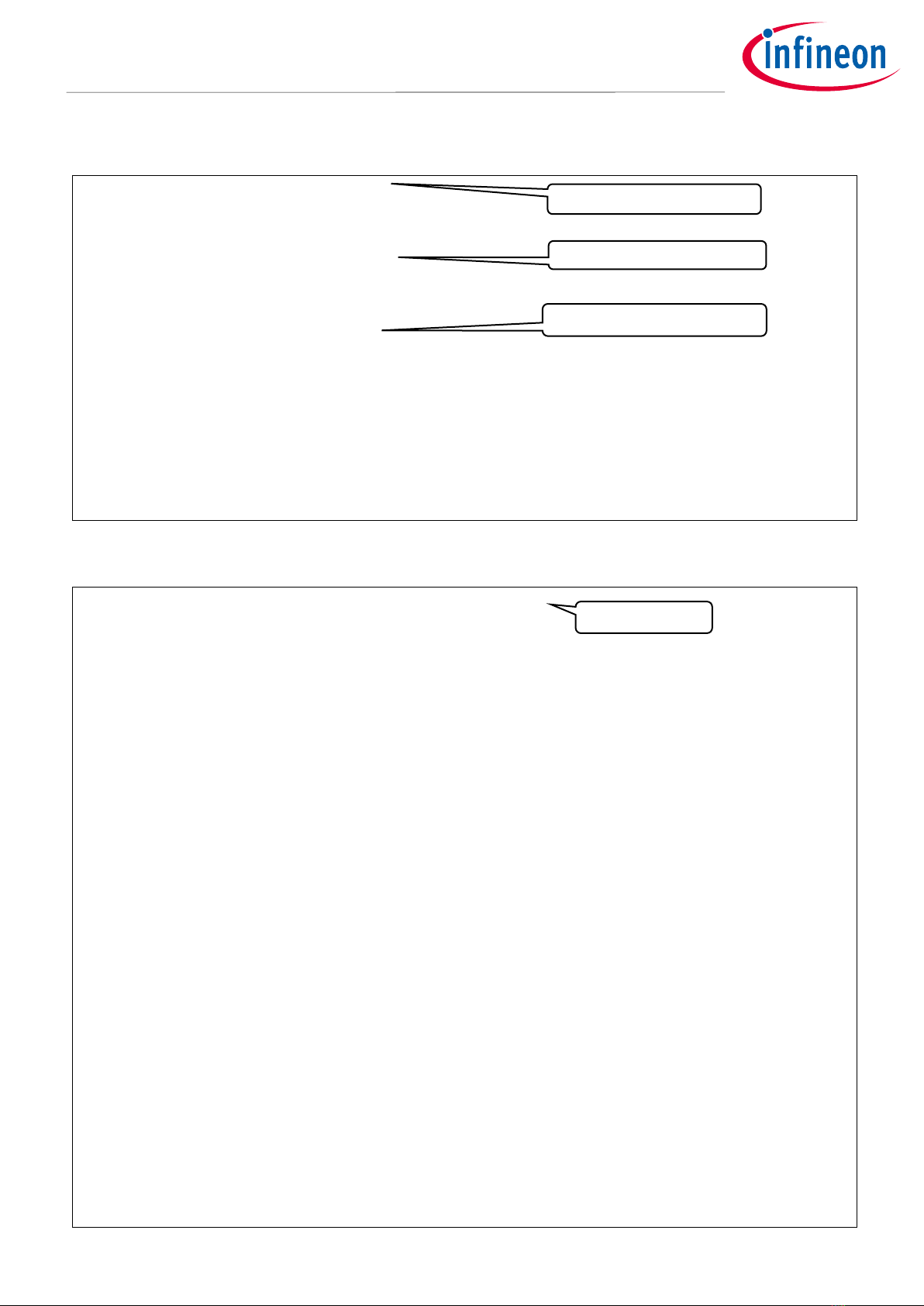
Figure 3 shows the distribution of the CLK_HF0.
The CLK_HF0 is the root clock for the CPU subsystem (CPUSS) and peripheral clock dividers. For details on
Figure 3, see the architecture TRM and datasheet.
CLK_TRC_DBG
CLK_GR3
CLK_MEM
PCLK
CLK_SLOW
SLOW_CLOCK_CTL register,
INT_DIV bit
Divider
(1-256)
CLK_HF0
CM0+
ROM / SRAM / Flash
CPUSS
slow infrastructure
P-DMA / M-DMA
CRYPTO
MEM_CLOCK_CTL register,
INT_DIV bit
Divider
(1-256)
PERI_GR3_CLOCK_CTL register,
INT_DIV bit
Divider
(1-256)
CLK_PERI
PERI_CLOCK_CTL register, INT_DIV
bit
Divider
(1-256)
Event generator
SMIF
CPUSS
fast infrastructure
SRSS
EFUSE
Ethernet
CLK_GR4
PERI_GR4_CLOCK_CTL register,
INT_DIV bit
Divider
(1-256)
IOSS
TCPWM[0]
CLK_GR8
PERI_GR8_CLOCK_CTL register,
INT_DIV bit
Divider
(1-256)
AUDIOSS
CPUSS(DEBUG)
TRC_DBG_CLOCK_CTL register,
INT_DIV bit
Divider
(1-256)
Peripheral
clock divider #0
PERI
VIDEOSS
Figure 3 Block diagram for CLK_HF0
CLK_MEM
Clock input to the CPUSS of the fast infrastructure, Ethernet, and serial
memory interface (SMIF)
CLK_PERI
Clock source for the CLK_GR and peripheral clock divider
CLK_SLOW
Clock input to the CPUSS of Cortex®-M0+ and slow infrastructure, SMIF, and
VIDEOSS
CLK_GR
Clock input to peripheral functions. The CLK_GR is grouped by the clock gater.
CLK_GR has six groups.
PCLK
Peripheral clock used in peripheral functions. The PCLK can be configured
each channel of IPs independently and select one divider to generate the
PCLK.
Application Note 8 of 80 002-26071 Rev. *B
2021-09-07
Clock configuration setup in TRAVEO™ T2G family CYT4D series MCUs
Clock system for TRAVEO™ T2G family MCUs
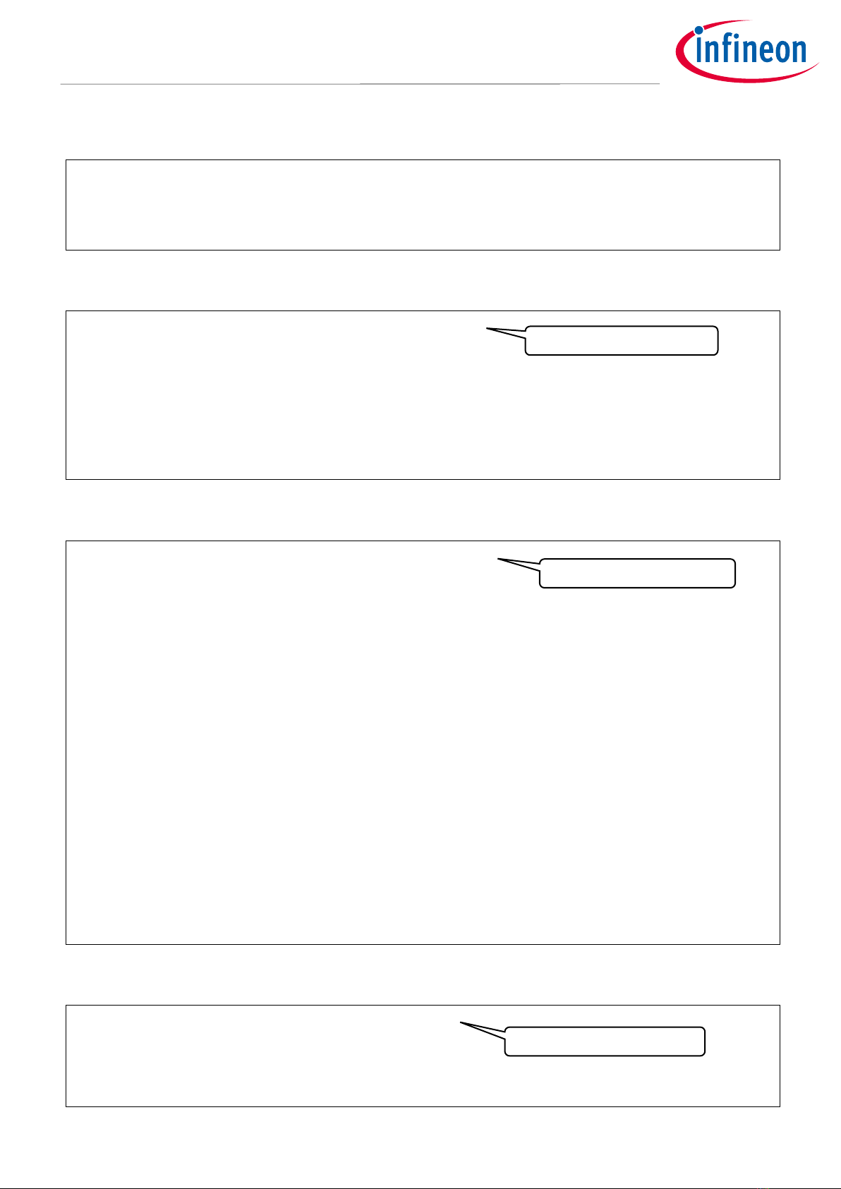
Figure 4 shows details of the peripheral clock divider #0.
These MCUs need a clock to each peripheral unit (say, the serial communication block (SCB), the timer,
counter, PWM (TCPWM), and so on) and its respective channel. These clocks are controlled by their respective
dividers.
This peripheral clock divider #0 has many peripheral clock dividers to generate the peripheral clock (PCLK). See
the datasheet for the number of dividers. The output of any of these dividers can be routed to any peripheral.
Note that dividers already in use cannot be used for other peripherals or channels.
PCLK
Clock divider
8.0
CLK_PERI
PERI_DIV_8_CTL register, INT8_DIV
bit
Clock divider
16.0
PERI_DIV_16_CTL register,
INT16_DIV bit
Clock divider
16.5
PERI_DIV_16_5_CTL register,
FRAC5_DIV bit & INT24_DIV bit
PERI_CLOCK_CTL register,
TYPE_SEL bit & DEV_SEL bit
9 dividers
16 dividers
7 dividers
124 mu ltiplexers
Clock
Generation
Clock divider
24.5
PERI_DIV_24_5_CTL register,
FRAC5_DIV bit & INT24_DIV bit
3 dividers
Clock enable multiplexing
Figure 4 Block diagram for the peripheral clock divider #0
CLK_TRC_DBG
Clock input to the CPUSS (DEBUG).
Divider
Divider has a function to divide each clock. It can be configured from 1 division
to 256 divisions.
Clock divider8.0
Divides a clock by 8
Clock divider16.0
Divides a clock by 16
Clock divider16.5
Divides a clock by 16.5
Clock divider24.5
Divides a clock by 24.5
Clock enable multiplexing
Enables the signal output from the clock divider
Clock generator
Divides the CLK_PERI based on the clock divider
Application Note 9 of 80 002-26071 Rev. *B
2021-09-07
Clock configuration setup in TRAVEO™ T2G family CYT4D series MCUs
Clock system for TRAVEO™ T2G family MCUs
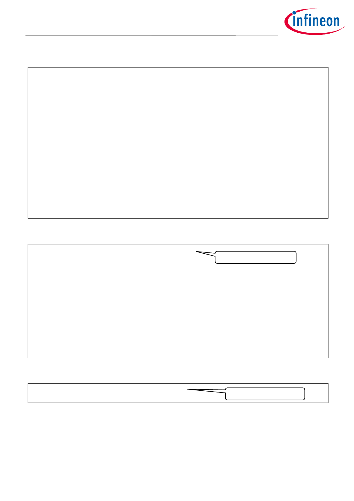
Figure 5 shows the distribution of the CLK_HF1.
The CLK_HF1 is a clock source of the CLK_FAST_0 and CLK_FAST_1. The clock distribution of the CLK_HF1 is
shown in Figure 5. The CLK_FAST_0 and CLK_FAST_1 are the input sources for CM7_0 and CM7_1 respectively.
CLK_FAST_0
CLK_HF1 CM7_0
FAST_0_CLOCK_CTL register,
INT_DIV bit
Divider
(1-256)
CLK_FAST_1 CM7_1
FAST_1_CLOCK_CTL register,
INT_DIV bit
Divider
(1-256)
Figure 5 Block diagram for the CLK_HF1
Figure 6 shows the distribution of the CLK_HF2, which is a clock source for the CLK_GR and PCLK.
CLK_GR5
PCLK
Peripheral
Clock Divider #1
PERI_GR5_CLOCK_CTLregister,
INT_DIV bit
Divider
(1-256)
LIN
CAN FD
CLK_GR6
PERI_GR6_CLOCK_CTL register,
INT_DIV bit
Divider
(1-256)
SCB
CLK_GR9
PERI_GR9_CLOCK_CTLregister,
INT_DIV bit
Divider
(1-256) SAR ADC
CLK_HF2
CXPI
Figure 6 Block diagram for the CLK_HF2
Application Note 10 of 80 002-26071 Rev. *B
2021-09-07
Clock configuration setup in TRAVEO™ T2G family CYT4D series MCUs
Clock system for TRAVEO™ T2G family MCUs
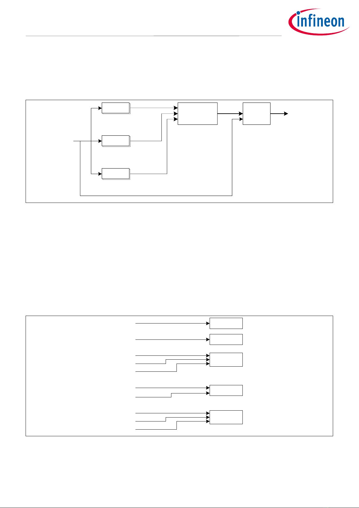
Figure 7 shows details of the peripheral clock divider #1.
The peripheral clock divider #1 has many peripheral clock dividers to generate the PCLK. See the datasheet for
the number of dividers. The output of any of these dividers can be routed to any peripheral. Note that the
dividers already in use cannot be used for other peripherals or channels.
PCLK
Clock divider
8.0
CLK_HF2
PERI_DIV_8_CTL register, INT8_DIV
bit
Clock enable multiplexing
Clock divider
16.0
PERI_DIV_16_CTL register,
INT16_DIV bit
Clock divider
24.5
PERI_DIV_24_5_CTL register,
FRAC5_DIV bit & INT24_DIV bit
PERI_CLOCK_CTLregister,
TYPE_SEL bit & DEV_SEL bit
3 dividers
4 dividers
7 dividers
124 mu ltiplexers
Clock
generation
Figure 7 Block diagram for the peripheral clock divider #1
Figure 8 shows the distribution of the CLK_HF3, CLK_HF4, CLK_HF5, CLK_HF6, CLK_HF7, CLK_HF8, CLK_HF9,
CLK_HF10, CLK_HF11, and CLK_HF12. For details on these functions in Figure 8, see the architecture TRM.
CLK_HF4 Ethernet
CLK_HF5 AUDIOSS
CLK_HF8
CLK_HF3 Event generator
SMIF
CLK_HF6
CLK_HF7
CLK_HF9
CLK_HF10 VIDEOSS
CLK_HF11
CLK_HF12
Figure 8 Block diagram for the CLK_HFx (x = 3 to 12)
The CLK_HF13 is dedicated to the CSV. See the architecture TRM for the CSV description.
Clock divider8.0
Divides a clock by 8
Clock divider16.0
Divides a clock by 16
Clock divider24.5
Divides a clock by 24.5
Clock enable multiplexing
Enables the signal output from the clock divider
Clock generator
Divides the CLK_PERI based on the clock divider

Application Note 11 of 80 002-26071 Rev. *B
2021-09-07
Clock configuration setup in TRAVEO™ T2G family CYT4D series MCUs
Clock system for TRAVEO™ T2G family MCUs
2.4 Basic clock system settings
This section describes how to configure the clock system based on a use case using the sample driver library
(SDL) provided by Infineon. The code snippets in this application note are part of the SDL. See Other
references.
The SDL has a configuration part and a driver part. The configuration part configures the parameter values for
the desired operation. The driver part configures each register based on the parameter values in the
configuration part. You can configure the configuration part according to your system.

Application Note 12 of 80 002-26071 Rev. *B
2021-09-07
Clock configuration setup in TRAVEO™ T2G family CYT4D series MCUs
Configuration of the clock resources
3Configuration of the clock resources
3.1 Setting the ECO
The ECO is disabled by default and needs to be enabled for usage. Also, trimming is necessary to use the ECO.
This device can configured with the trimming parameters that control the oscillator according to crystal unit
and ceramic resonator. The method to determine the parameters differs between the crystal unit and ceramic
resonator. See the Setting ECO parameters section in the TRAVEO™ T2G user guide for more information.
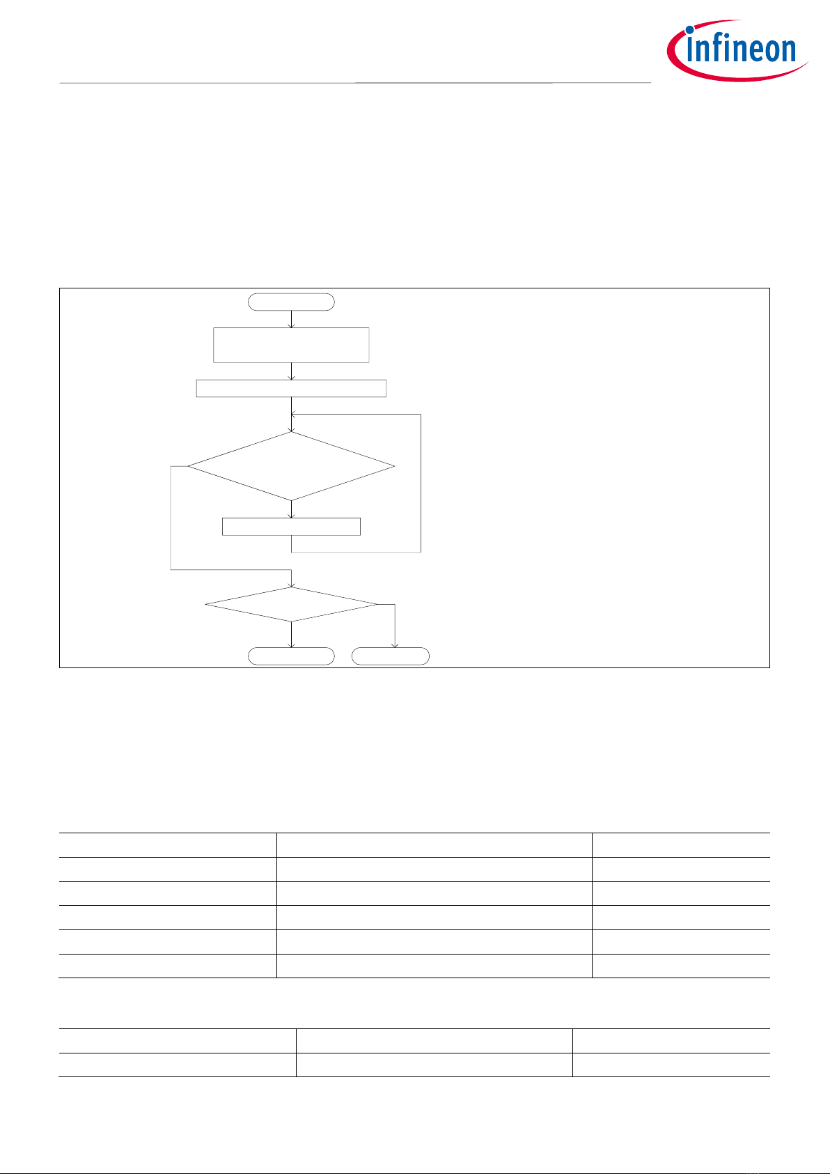
Figure 9 shows the ECO setting steps.
Start
Write "1" to ECO_EN
Check the state of
ECO_OK and the state of
TIMEOUT?
Yes
End(Success)
No
Define variable to count timeout
Configure the initial value of TIMEOUT
ECO_OK is already 1?
End(No change)
Define TIMEOUT variable
Configure TIMEOUT value
Write "1" to ECO_EN and to be available ECO
TIMEOUT= 0?
Subtract TIMEOUT value
End(Timeout)
Yes
No
No
Yes
Check whether the processing exited the loop at TIMEOUT
Configure trim Set ECO trimming data and AGC disabled
1. Calculate trim data
2. Trim settings by ECO user guide
(1)*
(2)
(3)
(4)
(5)
(6)
* Use to select the trimming data calculated by the software or the data calculated according to the ECO user guide.
Figure 9 Enabling the ECO

Application Note 13 of 80 002-26071 Rev. *B
2021-09-07
Clock configuration setup in TRAVEO™ T2G family CYT4D series MCUs
Configuration of the clock resources
3.1.1 Use case
•Oscillator to use: Crystal unit
•Fundamental frequency: 16 MHz
•Maximum drive level: 300.0 µW
•Equivalent series resistance: 150.0 ohm
•Shunt capacitance: 0.530 pF
•Parallel load capacitance: 8.000 pF
•Crystal unit vendor’s recommended value of negative resistance: 1500 ohm
•Automatic gain control: OFF
Note:These values are decided in consultation with the Crystal unit vendor.
3.1.2 Configuration
Table 1 lists the parameters and Table 2 lists the functions of the configuration part of in the SDL for ECO trim
settings.
Table 1 List of ECO trim settings parameters
Parameters
Description
Value
CLK_ECO_CONFIG2.WDTRIM
Watchdog trim
Calculated from Setting ECO parameters in
TRAVEO™ T2G user guide
7ul
CLK_ECO_CONFIG2.ATRIM
Amplitude trim
Calculated from Setting ECO parameters in
TRAVEO™ T2G user guide
0ul
CLK_ECO_CONFIG2.FTRIM
Filter trim of 3rd harmonic oscillation
Calculated from Setting ECO parameters in
TRAVEO™ T2G user guide
3ul
CLK_ECO_CONFIG2.RTRIM
Feedback resistor trim
Calculated from Setting ECO parameters in
TRAVEO™ T2G user guide
3ul
CLK_ECO_CONFIG2.GTRIM
Startup time of the gain trim
Calculated from Setting ECO parameters in
TRAVEO™ T2G user guide
3ul
CLK_ECO_CONFIG.AGC_EN
Automatic gain control (AGC) disabled
Calculated from Setting ECO parameters in
TRAVEO™ T2G user guide
0ul [OFF]
WAIT_FOR_STABILIZATION
Waiting for stabilization
10000ul
PLL_400M_0_PATH_NO
PLL number for PLL_400M_0
1ul
PLL_400M_1_PATH_NO
PLL number for PLL_400M_1
2ul
PLL_200M_0_PATH_NO
PLL number for PLL_200M_0
3ul
PLL_200M_1_PATH_NO
PLL number for PLL_200M_1
4ul
CLK_FREQ_ECO
Source clock frequency
16000000ul
SUM_LOAD_SHUNT_CAP_IN_PF
Sum of load shunt capacity (pF)
17ul

Application Note 14 of 80 002-26071 Rev. *B
2021-09-07
Clock configuration setup in TRAVEO™ T2G family CYT4D series MCUs
Configuration of the clock resources
Parameters
Description
Value
ESR_IN_OHM
Equivalent series resistance (ESR) (ohm)
250ul
MAX_DRIVE_LEVEL_IN_UW
Maximum drive level (uW)
100ul
MIN_NEG_RESISTANCE
Minimum negative resistance
5 * ESR_IN_OHM
Table 2 List of ECO trim settings functions
Functions
Description
Value
Cy_WDT_Disable()
Disable the watchdog timer
–
Cy_SysClk_FllDisable
Sequence(Wait Cycle)
Disable the FLL
Wait cycle =
WAIT_FOR_STABILIZATION
Cy_SysClk_Pll400M
Disable(PLL Number)
Disable the PLL400M_0
PLL number =
PLL_400M_0_PATH_NO
Disable the PLL400M_1
PLL number =
PLL_400M_1_PATH_NO
Cy_SysClk_PllDisable
(PLL Number)
Disable the PLL200M_0
PLL number =
PLL_200M_0_PATH_NO
Disable the PLL200M_1
PLL number =
PLL_200M_1_PATH_NO
AllClockConfiguration
()
Clock configuration
–
Cy_SysClk_EcoEnable
(Timeout value)
Set ECO enable and timeout value
Timeout value =
WAIT_FOR_STABILIZATION
Cy_SysLib_DelayUs(Wait
Time)
Delay by the specified number of
microseconds
Wait time = 1u (1us)
3.1.3 Sample code for initial ECO configuration
Code Listing 1 provides a sample code.
The following description will help you understand the register notation of the driver part of the SDL:
•SRSS->unCLK_ECO_CONFIG.stcField.u1ECO_EN is the SRSS_CLK_ECO_CONFIG.ECO_EN mentioned in the
Registers TRM. Other registers are also described in the same manner.
•Performance improvement measures
To improve the performance of register setting, the SDL writes a complete 32-bit data to the register. Each
bit field is generated in advance in a bit-writable buffer and written to the register as the final 32-bit data.
tempTrimEcoCtlReg.u32Register = SRSS->unCLK_ECO_CONFIG2.u32Register;
tempTrimEcoCtlReg.stcField.u3WDTRIM = wdtrim;
tempTrimEcoCtlReg.stcField.u4ATRIM = atrim;
tempTrimEcoCtlReg.stcField.u2FTRIM = ftrim;
tempTrimEcoCtlReg.stcField.u2RTRIM = rtrim;
tempTrimEcoCtlReg.stcField.u3GTRIM = gtrim;
SRSS->unCLK_ECO_CONFIG2.u32Register = tempTrimEcoCtlReg.u32Register;
See cyip_srss_v2.h under hdr/rev_x/ip for more information on the union and structure representation of
registers.
Application Note 15 of 80 002-26071 Rev. *B
2021-09-07
Clock configuration setup in TRAVEO™ T2G family CYT4D series MCUs
Configuration of the clock resources
Code Listing 1 General configuration of ECO settings
:
/** Wait time definition **/
#define WAIT_FOR_STABILIZATION (10000ul)
:
#define CLK_FREQ_ECO (16000000ul)
:
#define PLL_400M_0_PATH_NO (1ul)
#define PLL_400M_1_PATH_NO (2ul)
#define PLL_200M_0_PATH_NO (3ul)
#define PLL_200M_1_PATH_NO (4ul)
:
#define SUM_LOAD_SHUNT_CAP_IN_PF (17ul)
:
#define ESR_IN_OHM (250ul)
:
#define MIN_NEG_RESISTANCE (5 * ESR_IN_OHM)
#define MAX_DRIVE_LEVEL_IN_UW (100ul)
:
static void AllClockConfiguration(void);
:
int main(void)
{
/* disable watchdog timer */
Cy_WDT_Disable();
:
/* Disable Fll */
CY_ASSERT(Cy_SysClk_FllDisableSequence(WAIT_FOR_STABILIZATION) == CY_SYSCLK_SUCCESS);
/* Disable Pll */
CY_ASSERT(Cy_SysClk_Pll400MDisable(PLL_400M_0_PATH_NO) == CY_SYSCLK_SUCCESS);
CY_ASSERT(Cy_SysClk_Pll400MDisable(PLL_400M_1_PATH_NO) == CY_SYSCLK_SUCCESS);
CY_ASSERT(Cy_SysClk_PllDisable(PLL_200M_0_PATH_NO) == CY_SYSCLK_SUCCESS);
CY_ASSERT(Cy_SysClk_PllDisable(PLL_200M_1_PATH_NO) == CY_SYSCLK_SUCCESS);
/* Enable interrupt */
__enable_irq();
/* Set Clock Configuring registers */
AllClockConfiguration();
:
/* Please ensure output clock frequency using oscilloscope */
for(;;);
}
Code Listing 2 AllClockConfiguration() function
static void AllClockConfiguration(void)
{
:
/***** ECO setting ******/
cy_en_sysclk_status_t ecoStatus;
ecoStatus = Cy_SysClk_EcoConfigureWithMinRneg(
CLK_FREQ_ECO,
SUM_LOAD_SHUNT_CAP_IN_PF,
ESR_IN_OHM,
MAX_DRIVE_LEVEL_IN_UW,
MIN_NEG_RESISTANCE
);
CY_ASSERT(ecoStatus == CY_SYSCLK_SUCCESS);
{
SRSS->unCLK_ECO_CONFIG2.stcField.u3WDTRIM = 7ul;
SRSS->unCLK_ECO_CONFIG2.stcField.u4ATRIM = 0ul;
SRSS->unCLK_ECO_CONFIG2.stcField.u2FTRIM = 3ul;
SRSS->unCLK_ECO_CONFIG2.stcField.u2RTRIM = 3ul;
SRSS->unCLK_ECO_CONFIG2.stcField.u3GTRIM = 0ul;
SRSS->unCLK_ECO_CONFIG.stcField.u1AGC_EN = 0ul;
ecoStatus = Cy_SysClk_EcoEnable(WAIT_FOR_STABILIZATION);
CY_ASSERT(ecoStatus == CY_SYSCLK_SUCCESS);
}
:
return;
}
Either (1)-1 or (1)-2 can be used.
Comment out or delete unused code snippets in (1)-1 or (1)-2.
Define the TIMEOUT variable.
Define the oscillator parameters to use for software calculation.
Define the PLL number.
Watchdog timer disable
Disable the FLL.
Disable the PLL.
Trim and ECO setting. See Code Listing 2.
(1)-1. Trim settings for software calculation.
See Code Listing 4.
(1)-2. Trim settings according to the ECO user guide
ECO enable. See Code Listing 3.

Application Note 16 of 80 002-26071 Rev. *B
2021-09-07
Clock configuration setup in TRAVEO™ T2G family CYT4D series MCUs
Configuration of the clock resources
Code Listing 3 Cy_SysClk_EcoEnable() function
cy_en_sysclk_status_t Cy_SysClk_EcoEnable(uint32_t timeoutus)
{
cy_en_sysclk_status_t rtnval;
/* invalid state error if ECO is already enabled */
if (SRSS->unCLK_ECO_CONFIG.stcField.u1ECO_EN != 0ul) /* 1 = enabled */
{
return CY_SYSCLK_INVALID_STATE;
}
/* first set ECO enable */
SRSS->unCLK_ECO_CONFIG.stcField.u1ECO_EN = 1ul; /* 1 = enable */
/* now do the timeout wait for ECO_STATUS, bit ECO_OK */
for (;
(SRSS->unCLK_ECO_STATUS.stcField.u1ECO_OK == 0ul) &&(timeoutus != 0ul);
timeoutus--)
{
Cy_SysLib_DelayUs(1u);
}
rtnval = ((timeoutus == 0ul) ? CY_SYSCLK_TIMEOUT : CY_SYSCLK_SUCCESS);
return rtnval;
}
Code Listing 4 Cy_SysClk_EcoConfigureWithMinRneg() function
cy_en_sysclk_status_t Cy_SysClk_EcoConfigureWithMinRneg(uint32_t freq, uint32_t cSum, uint32_t esr, uint32_t
driveLevel, uint32_t minRneg)
{
/* Check if ECO is disabled */
if(SRSS->unCLK_ECO_CONFIG.stcField.u1ECO_EN == 1ul)
{
return(CY_SYSCLK_INVALID_STATE);
}
/* calculate intermediate values */
float32_t freqMHz = (float32_t)freq / 1000000.0f;
float32_t maxAmplitude = (1000.0f * ((float32_t)sqrt((float64_t)((float32_t)driveLevel / (2.0f *
(float32_t)esr))))) /
(M_PI * freqMHz * (float32_t)cSum);
float32_t gm_min = (157.91367042f /*4 * M_PI * M_PI * 4*/ * minRneg * freqMHz * freqMHz * (float32_t)cSum *
(float32_t)cSum) /
1000000000.0f;
/* Get trim values according to caluculated values */
uint32_t atrim, agcen, wdtrim, gtrim, rtrim, ftrim;
atrim = Cy_SysClk_SelectEcoAtrim(maxAmplitude);
if(atrim == CY_SYSCLK_INVALID_TRIM_VALUE)
{
return(CY_SYSCLK_BAD_PARAM);
}
agcen = Cy_SysClk_SelectEcoAGCEN(maxAmplitude);
if(agcen == CY_SYSCLK_INVALID_TRIM_VALUE)
{
return(CY_SYSCLK_BAD_PARAM);
}
wdtrim = Cy_SysClk_SelectEcoWDtrim(maxAmplitude);
if(wdtrim == CY_SYSCLK_INVALID_TRIM_VALUE)
{
return(CY_SYSCLK_BAD_PARAM);
}
(2) Check if ECO_OK is already enabled.
(3) Write “1” to the ECO_EN bit, and
make ECO available.
(4) Check the state of ECO_OK
and the state of TIMEOUT.
(5) Subtract the TIMEOUT value.
Wait for 1 us.
(6) Check whether processing exited the
loop at TIMEOUT.
Trim calculation by software
Get the Atrim value. See Code Listing 5.
Get the AGC enable setting. See Code Listing 6.
Get the Wdtrim value. See Code Listing 7.
Application Note 17 of 80 002-26071 Rev. *B
2021-09-07
Clock configuration setup in TRAVEO™ T2G family CYT4D series MCUs
Configuration of the clock resources
Code Listing 4 Cy_SysClk_EcoConfigureWithMinRneg() function
gtrim = Cy_SysClk_SelectEcoGtrim(gm_min);
if(gtrim == CY_SYSCLK_INVALID_TRIM_VALUE)
{
return(CY_SYSCLK_BAD_PARAM);
}
rtrim = Cy_SysClk_SelectEcoRtrim(freqMHz);
if(rtrim == CY_SYSCLK_INVALID_TRIM_VALUE)
{
return(CY_SYSCLK_BAD_PARAM);
}
ftrim = Cy_SysClk_SelectEcoFtrim(atrim);
/* update all fields of trim control register with one write, without changing the ITRIM field: */
un_CLK_ECO_CONFIG2_t tempTrimEcoCtlReg;
tempTrimEcoCtlReg.u32Register = SRSS->unCLK_ECO_CONFIG2.u32Register;
tempTrimEcoCtlReg.stcField.u3WDTRIM = wdtrim;
tempTrimEcoCtlReg.stcField.u4ATRIM = atrim;
tempTrimEcoCtlReg.stcField.u2FTRIM = ftrim;
tempTrimEcoCtlReg.stcField.u2RTRIM = rtrim;
tempTrimEcoCtlReg.stcField.u3GTRIM = gtrim;
SRSS->unCLK_ECO_CONFIG2.u32Register = tempTrimEcoCtlReg.u32Register;
SRSS->unCLK_ECO_CONFIG.stcField.u1AGC_EN = agcen;
return(CY_SYSCLK_SUCCESS);
}
Code Listing 5 Cy_SysClk_SelectEcoAtrim () function
__STATIC_INLINE uint32_t Cy_SysClk_SelectEcoAtrim(float32_t maxAmplitude)
{
if((0.50f <= maxAmplitude) && (maxAmplitude < 0.55f))
{
return(0x04ul);
}
else if(maxAmplitude < 0.60f)
{
return(0x05ul);
}
else if(maxAmplitude < 0.65f)
{
return(0x06ul);
}
else if(maxAmplitude < 0.70f)
{
return(0x07ul);
}
else if(maxAmplitude < 0.75f)
{
return(0x08ul);
}
else if(maxAmplitude < 0.80f)
{
return(0x09ul);
}
else if(maxAmplitude < 0.85f)
{
return(0x0Aul);
}
else if(maxAmplitude < 0.90f)
{
return(0x0Bul);
}
else if(maxAmplitude < 0.95f)
{
return(0x0Cul);
}
else if(maxAmplitude < 1.00f)
{
return(0x0Dul);
}
else if(maxAmplitude < 1.05f)
{
return(0x0Eul);
}
else if(maxAmplitude < 1.10f)
{
return(0x0Ful);
}
else if(1.1f <= maxAmplitude)
{
Get the Gtrim value. See Code Listing 8.
Get then Rtrim value. See Code Listing 9.
Get the Ftrim value. See Code Listing 10.
Get the Atrim value.
Application Note 18 of 80 002-26071 Rev. *B
2021-09-07
Clock configuration setup in TRAVEO™ T2G family CYT4D series MCUs
Configuration of the clock resources
Code Listing 5 Cy_SysClk_SelectEcoAtrim () function
return(0x00ul);
}
else
{
// invalid input
return(CY_SYSCLK_INVALID_TRIM_VALUE);
}
}
Code Listing 6 Cy_SysClk_SelectEcoAGCEN() function
__STATIC_INLINE uint32_t Cy_SysClk_SelectEcoAGCEN(float32_t maxAmplitude)
{
if((0.50f <= maxAmplitude) && (maxAmplitude < 1.10f))
{
return(0x01ul);
}
else if(1.10f <= maxAmplitude)
{
return(0x00ul);
}
else
{
return(CY_SYSCLK_INVALID_TRIM_VALUE);
}
}
Code Listing 7 Cy_SysClk_SelectEcoWDtrim() function
__STATIC_INLINE uint32_t Cy_SysClk_SelectEcoWDtrim(float32_t amplitude)
{
if( (0.50f <= amplitude) && (amplitude < 0.60f))
{
return(0x02ul);
}
else if(amplitude < 0.7f)
{
return(0x03ul);
}
else if(amplitude < 0.8f)
{
return(0x04ul);
}
else if(amplitude < 0.9f)
{
return(0x05ul);
}
else if(amplitude < 1.0f)
{
return(0x06ul);
}
else if(amplitude < 1.1f)
{
return(0x07ul);
}
else if(1.1f <= amplitude)
{
return(0x07ul);
}
else
{
// invalid input
return(CY_SYSCLK_INVALID_TRIM_VALUE);
}
}
Code Listing 8 Cy_SysClk_SelectEcoGtrim() function
__STATIC_INLINE uint32_t Cy_SysClk_SelectEcoGtrim(float32_t gm_min)
{
if( (0.0f <= gm_min) && (gm_min < 2.2f))
{
return(0x00ul+1ul);
}
else if(gm_min < 4.4f)
{
return(0x01ul+1ul);
Get the AGC enable setting.
Get the Wdtrim value.
Get the Gtrim value.
Application Note 19 of 80 002-26071 Rev. *B
2021-09-07
Clock configuration setup in TRAVEO™ T2G family CYT4D series MCUs
Configuration of the clock resources
Code Listing 8 Cy_SysClk_SelectEcoGtrim() function
}
else if(gm_min < 6.6f)
{
return(0x02ul+1ul);
}
else if(gm_min < 8.8f)
{
return(0x03ul+1ul);
}
else if(gm_min < 11.0f)
{
return(0x04ul+1ul);
}
else if(gm_min < 13.2f)
{
return(0x05ul+1ul);
}
else if(gm_min < 15.4f)
{
return(0x06ul+1ul);
}
else if(gm_min < 17.6f)
{
// invalid input
return(CY_SYSCLK_INVALID_TRIM_VALUE);
}
else
{
// invalid input
return(CY_SYSCLK_INVALID_TRIM_VALUE);
}
}
Code Listing 9 Cy_SysClk_SelectEcoRtrim() function
__STATIC_INLINE uint32_t Cy_SysClk_SelectEcoRtrim(float32_t freqMHz)
{
if(freqMHz > 28.6f)
{
return(0x00ul);
}
else if(freqMHz > 23.33f)
{
return(0x01ul);
}
else if(freqMHz > 16.5f)
{
return(0x02ul);
}
else if(freqMHz > 0.0f)
{
return(0x03ul);
}
else
{
// invalid input
return(CY_SYSCLK_INVALID_TRIM_VALUE);
}
}
Code Listing 10 Cy_SysClk_SelectEcoFtrim() function
__STATIC_INLINE uint32_t Cy_SysClk_SelectEcoFtrim(uint32_t atrim)
{
return(0x03ul);
}
Get the Rtrim value.
Get the Ftrim value.
Application Note 20 of 80 002-26071 Rev. *B
2021-09-07
Clock configuration setup in TRAVEO™ T2G family CYT4D series MCUs
Configuration of the clock resources
3.2 Setting WCO
3.2.1 Operation overview
The WCO is disabled by default. Accordingly, the WCO cannot be used unless it is enabled. Figure 10 shows how
to configure registers for enabling the WCO.
To disable the WCO, write ‘0’ to the WCO_EN bit of the BACKUP_CTL register.
Start
Write "1" to the WCO_EN bit
Check the state
of WCO_OK and the state of TIMEOUT ?
Yes
End(Success)
No
Define variable to count timeout
Configure the initial value of TIMEOUT
Define variables TIMEOUT
Configure TIMEOUT value
Write "1" to the WCO_EN bit, and make WCO available
TIMEOUT= 0?
Subtract TIMEOUT value
End(Timeout)
Yes
No
Check whether the processing exited the loop at TIMEOUT
(1)
(2)
(3)
(4)
Figure 10 Enabling WCO
3.2.2 Configuration
Table 3 lists the parameters and Table 4 lists the functions of the configuration part of in the SDL for WCO
settings.
Table 3 List of WCO settings parameters
Parameters
Description
Value
WAIT_FOR_STABILIZATION
Waiting for stabilization
10000ul
PLL_400M_0_PATH_NO
PLL number for PLL_400M_0
1ul
PLL_400M_1_PATH_NO
PLL number for PLL_400M_1
2ul
PLL_200M_0_PATH_NO
PLL number for PLL_200M_0
3ul
PLL_200M_1_PATH_NO
PLL number for PLL_200M_1
4ul
Table 4 List of WCO settings functions
Functions
Description
Value
Cy_WDT_Disable()
Disable the watchdog timer
–
Table of contents
Popular Clock manuals by other brands

Adaptive Micro Systems
Adaptive Micro Systems Alpha user manual

Chaney Instrument
Chaney Instrument Atomic Clock instruction manual

La Crosse Technology
La Crosse Technology C75723-AU Setup guide

Masterclock
Masterclock NTD200 user manual

ADE
ADE CK 2308 operating instructions

American Time
American Time SiteSync IQ Quick start installation guide


Ambient Weather
Ambient Weather Fischer Instruments 1434TD-22 user manual

OzSpy
OzSpy HDESKX10 Quick reference guide

La Crosse Technology
La Crosse Technology 513-1417ALv4 quick start guide

procontrol
procontrol Church Clock manual

BANGGOOD
BANGGOOD ECL-132 manual

Mobatime
Mobatime DC Series instruction manual