Infineon D2 PAK User manual

User Guide Please read the Important Notice and Warnings at the end of this document Revision 1.0
www.infineon.com 2018-03-01
UG_1801_PL16_1802_225559
Full-bridge converter for UPS
D2PAK/D2PAK-7 kit
About this document
This user guide describes the Infineon full-bridge demo board for UPS. The current design considers only the
power section including drivers and power devices with D2packages. D27-pin packages can also be used in this
demo board, which enables users to evaluate the performance of power MOSFETs and their drivers.
Scope and purpose
This document is intended to describe the functionalities of UPS converting DC to AC voltages. Users can then
evaluate the performance of power MOSFETs with gate driver ICs. With Infineon low-RDS(on) MOSFETs the demo
board can help reduce system cost and time-to-market.
Intended audience
This document addresses the market for UPS manufacturers with the goal of providing a high-performance
system solution at low cost.
Table of contents
About this document ............................................................................................................................1
Table of contents..................................................................................................................................1
1 Full-bridge converter for UPS with D2PAK/D2PAK-7 kit .......................................................... 2
1.1 Overview ............................................................................................................................................2
1.1.1 Key features ..................................................................................................................................3
1.2 Schematic ..........................................................................................................................................4
1.3 Layout ................................................................................................................................................4
1.4 Power-up procedure...........................................................................................................................6
1.4.1 PWM signal selections...................................................................................................................6
1.5 Performance evaluations....................................................................................................................6
1.5.1 Performance with heatsink at the front .........................................................................................6
1.5.2 Performance with heatsink at the back .......................................................................................10
1.6 Power loss estimations of MOSFETs and CS resistor ........................................................................ 11
1.7 Bill of Materials (BOM) ..................................................................................................................... 13
1.8 Additional results with D2PAK-7 (IRFS7430-7P).................................................................................14
1.8.1 Performance with heatsink at the back with 420 W load .............................................................14
1.8.2 Performance with heatsink at the back with 500 W .....................................................................15
1.8.3 Performance with heatsink at the front with 500 W..................................................................... 17
Revision history ..................................................................................................................................19

User Guide 2 Revision 1.0
2018-03-01
Full-bridge converter for UPS
D2PAK/ D2PAK-7 kit
UG_1801_PL16_1802_225559
1 Full-bridge converter for UPS with D2PAK/D2PAK-7 kit
1.1 Overview
The full-bridge converter kit is a demo board for UPS applications. It contains two sections of half-bridge drivers
and power devices, as shown in Figure 1.
Figure 1 Full-bridge converter demo board (120 mm ×120 mm)
The demo board needs two power supplies to provide an input voltage and a bias voltage. The voltages of both
power supplies are typically 12 V, which can be changed based on an application. The outputs can be connected
to a transformer. In this user guide, a transformer is used to get an AC voltage of 220 V with the input voltage of
12 V. In order to power up the demo board, two synchronized PWM signals are needed to control switching of
four power MOSFETs.
Vin+
Vin-
Vout2
Vout1
Vbias+ Vbias-
- +
PWM1 + -
PWM2

User Guide 3 Revision 1.0
2018-03-01
Full-bridge converter for UPS
D2PAK/ D2PAK-7 kit
UG_1801_PL16_1802_225559
1.1.1 Key features
The capabilities of the full-bridge converter for UPS with D2/D27-pin kit are as follows:
•D2/D27-pin kit for MOSFETs
•Separate Vin and bias voltages (12 V is used in this user guide)
•600 V gate driver IC with +/- 4 A peak drive current (IRS2186)
•Current Sense (CS) information
•A heatsink can be mounted with four screws, which can be placed at the back or at the front
Figure 2 Heatsink (4 × 2.5 × 0.5 inches) mounted at the front or back with thermal pad
(Heatsink: ACCEL Thermal 914; Thermal pad: Berguist Gap Pad 5000S35, 20 mils)
User Guide 4 Revision 1.0
2018-03-01
Full-bridge converter for UPS
D2PAK/ D2PAK-7 kit
UG_1801_PL16_1802_225559
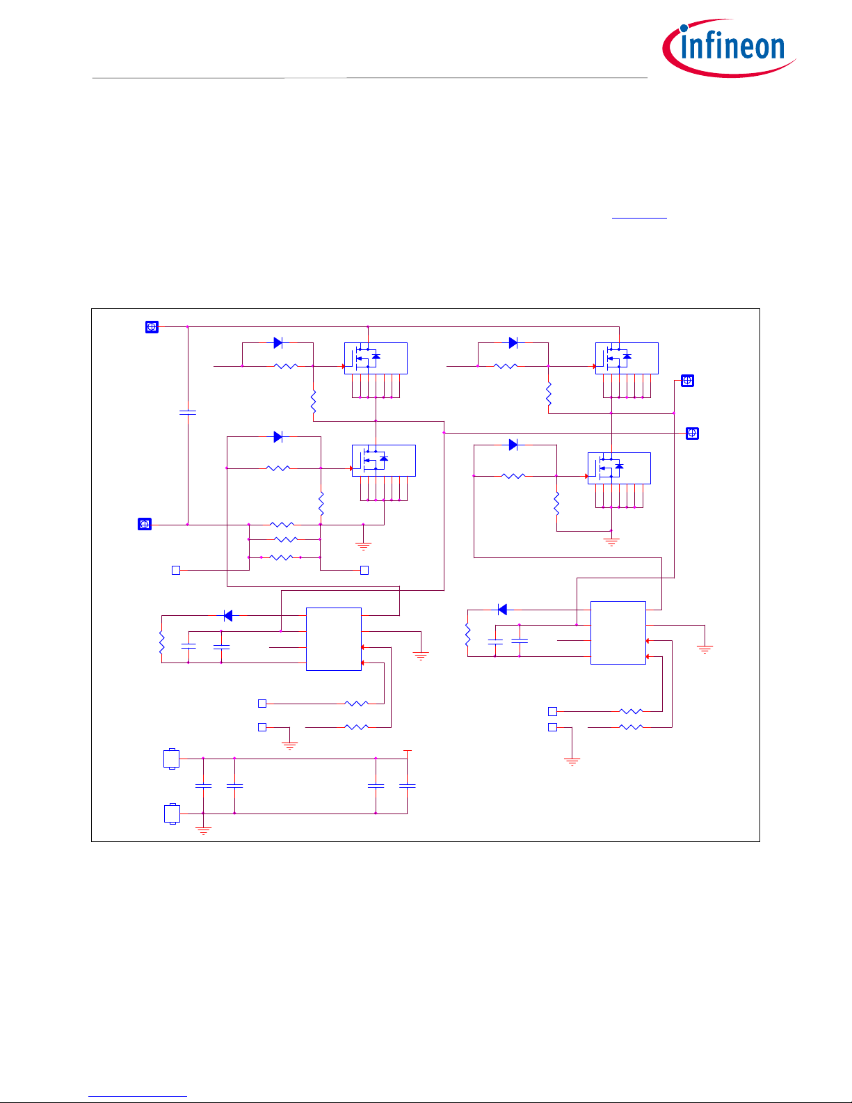
1.2 Schematic
A schematic of the demo board is shown in Figure 3. In the demo board, four MOSFETs (IRFS7430) are used. D27-
pin packages can be used if they are desired for evaluation. Two IRS2186 drivers are used to drive four MOSFETs.
Only two PWM signals are needed to control timing of the switching of the four MOSFETs. D1~4 four diodes are
used to have a slow turn-off to avoid high Vds spike during turn-off.
Figure 3 Schematic of the demo board
1.3 Layout
The demo board PCB has only two layers, as shown in Figure 4. Fabricated with FR4 material, both layers are 2
oz. copper with a board thickness of 62 mils (1.58 mm).
+
C1
2700uFx50V
+
C6
47 uF, 35V
C8
0.1uF 50V
C7
0.1uF 50V
D1
1 2
D2
1 2
D3
1 2
D4
1 2
+
C4
47 uF, 50V
D5 12 U2
IRS2186SPBF
Vb
8HO
7
LO 4
COM 3
Vcc
5
Vs
6
LIN 2
HIN 1
R1 47
R2 47
R3 47
R4 47
R5
10 K
R6
10 K
R7
10 K
R8
10 K
R13 1mOhm
R14 open
C9
0.1uF 50V
C10
0.1uF 50V
Top_Q1_S
HOV1
BIAS+15V
G_Q1
G_Q4
TP1
PWM1
TP2
GND
TP3
PWM2
TP4
GND
PWM1
PWM2
R15
1.2
R16
1.2
R12 5.1
PWM2
VbU1
BIAS +15V
R17 open
Top_Q2_S
G_Q2HOV2
PRTN
PowerIN
PRTN
Vout1
Vout2
PWM1
TP5
PRNT TP6
GND
PRTN
HOV2
VbU2
BIAS +15V
+
C5
47 uF, 35V
+
C3
47uF, 50V
Q1
IRFS7430
1
4
2
39
5
6
7
8
Q3
IRFS7430
1
4
2
39
5
6
7
8
D6 12 U1
IRS2186SPBF
Vb
8HO
7
LO 4
COM 3
Vcc
5
Vs
6
LIN 2
HIN 1
Q2
IRFS7430
1
4
2
39
5
6
7
8
HOV1
Q4
IRFS7430
1
4
2
39
5
6
7
8
BIAS +15V
G_Q3
PowerIN
R11 5.1
R10 5.1
R9 5.1
J2
BIAS +15V
J3
GND

User Guide 5 Revision 1.0
2018-03-01
Full-bridge converter for UPS
D2PAK/ D2PAK-7 kit
UG_1801_PL16_1802_225559
Top
Bottom
Figure 4 PCB top and bottom layers
User Guide 6 Revision 1.0
2018-03-01
Full-bridge converter for UPS
D2PAK/ D2PAK-7 kit
UG_1801_PL16_1802_225559
1.4 Power-up procedure
Always connect the bias, two PWM signals and load first, then increase the input voltage from zero.
1.4.1 PWM signal selections
This user guide describes a set-up providing a 50 Hz square-wave AC output. Therefore, both PWM signals are
set with 50 Hz. The dead-time between the two legs has to be set high enough that the reset of the transformer
is completed. A shorter dead-time increases total turn-on time, which may saturate the transformer. A value of
0.9 ms was selected to do the tests. Both PWM signals have an amplitude of 10 V.
1.5 Performance evaluations
Test conditions:
Vin: 12 V
Vbias: 12 V
PWM 1, 2: 50 Hz, 10 V, with 10 ms delay between them plus 0.7 ms dead-time
Load: Transformer (primary connected to Vout1 and Vout2, secondary connected to incandescent light
bulbs, load of 420 W)
Airflow: No
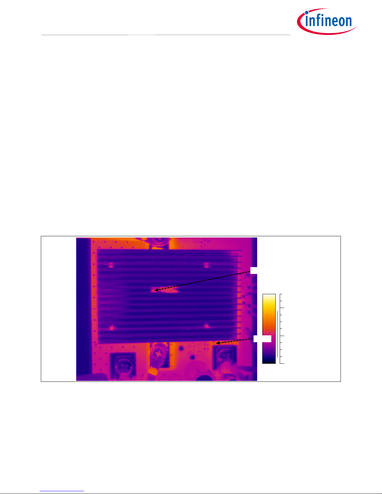
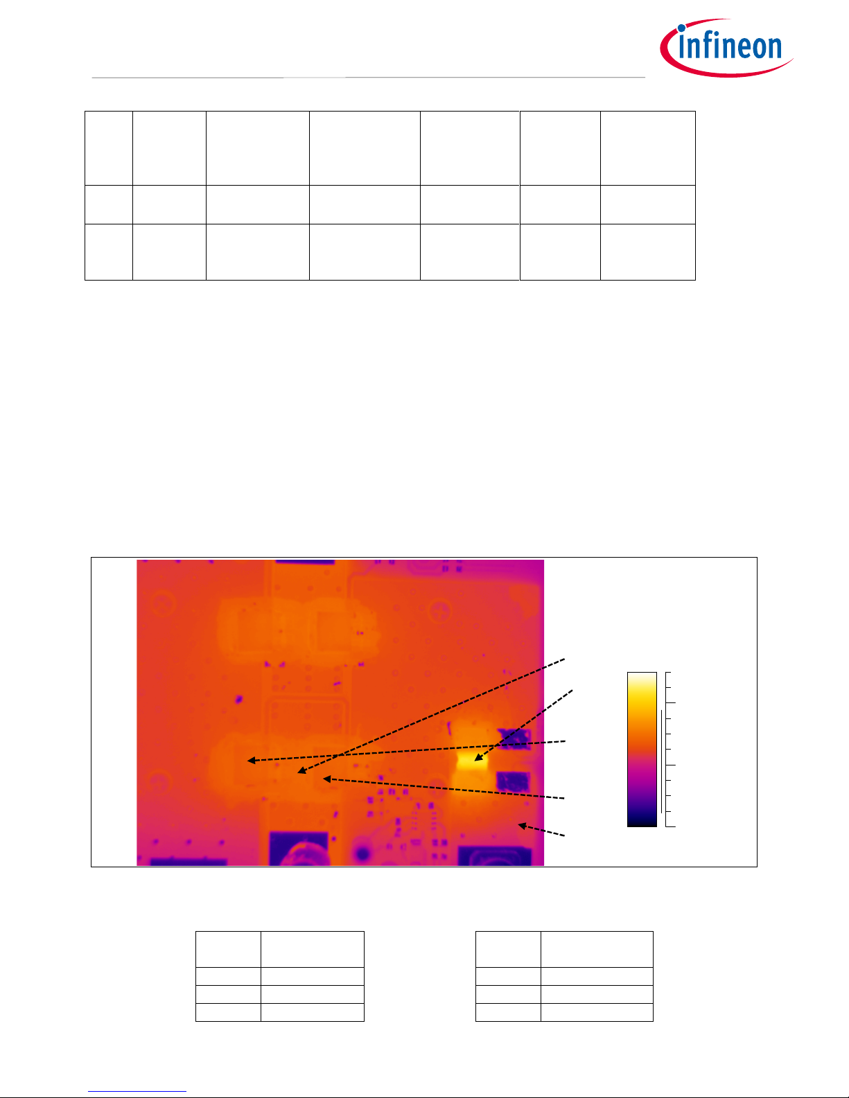
1.5.1 Performance with heatsink at the front
Figure 5 Front thermal image after 1 hour
20.0°C
70.0°C
20
40
60
43
°
C
A:45
°
C
User Guide 7 Revision 1.0
2018-03-01
Full-bridge converter for UPS
D2PAK/ D2PAK-7 kit
UG_1801_PL16_1802_225559
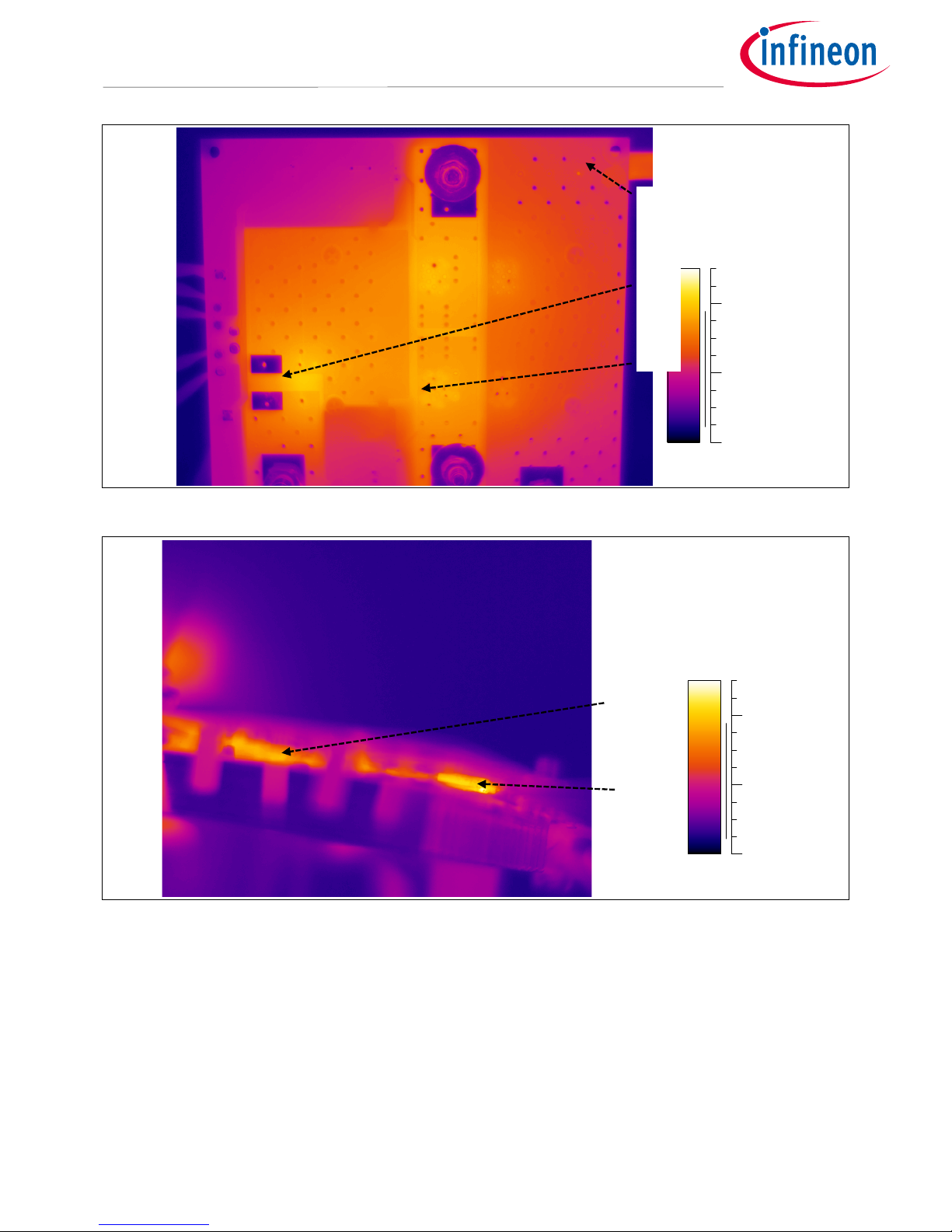
Figure 6 Back thermal image after 1 hour
Figure 7 Side thermal image after 1 hr
Comparing the temperature readings at points A and B between the front and back sides at the corner in Figures
6 and 7 shows that they are the same. Case temperatures of the MOSFETs are 1°C higher at the front than at the
back, as shown in Figures, 6, 7 and 8.
20.0°C
70.0°C
20
40
60
20.0°C
70.0°C
20
40
60
B:45
°
C
60°C
57°C
58°C
(FET)
68°C
Resistor

User Guide 8 Revision 1.0
2018-03-01
Full-bridge converter for UPS
D2PAK/ D2PAK-7 kit
UG_1801_PL16_1802_225559
Figure 8 Typical input and output power measurement after 1 hour
Table 1 Efficiency after 1 hour
No.
Effic
ie
ncy
(percent)
1
96.5
2
96.5
3
96.5
4
96.7
5
96.6
6
96.7
7
96.3
8
96.3
Ave
rage
96.5
Stdev
0.1
The average efficiency shown in Table 1 is 96.5 percent at 420 W load. The average total power loss is about 13
W. The reset time for the transformer is about 20 µs, as shown in Figure 9, which is much less than the dead-time
of 700 µs. The MOSFET turn-off waveforms are shown in Figure 10. Since Ids was measured by a Rogowski coil
current probe (C2), its zero level has an offset (I22 = -25 A), as shown in Figure 11. The turn-off switching power
loss can be calculated as:
f(Hz)×∫[()− 22] ∙ ()
=f(Hz) × [(F12 - F11 - I22.(F22 - F21)]
= 50 Hz ×|(116 µJ – (25 × 16.7 µ))| = 15 mW.
The turn-off switching power loss for Q2, 3 and 4 is 16, 17 and 13 mW, respectively. Therefore, switching power
losses are negligible.
C1: Iout (20 A/div)
C2: Vout2 - Vout1
(10 V/div)
C3: Iin (20 A/div)
C4: V
in
(5 V/div)

User Guide 9 Revision 1.0
2018-03-01
Full-bridge converter for UPS
D2PAK/ D2PAK-7 kit
UG_1801_PL16_1802_225559
Figure 9 Waveforms during the dead-time
t1 t2
Figure 10 Turn-off waveforms
C1: Vout1 - Vout2 (5 V
/div)
C2: IIoad (0.5 A/div)
C3: Vds3 (5 V/div)
C4: V
ds4
(5 V/div)
↔
2
0 µ
s
(reset)
C1: Itr (20 A/div)
C2: Ids_Q1 (10 A
/div)
C4: V
ds_Q1
(5 V/div)
27V
C2
1
=
0.27 V (I21 = 27 A)
C22
=
-
0.25 V (I22 =
-
25 A)
F1:
Integral
of C4 x
C2
(power), F11 = 4.9 µJ, F12 = 121 µJ,
∆F1 = 116 µJ
F2: Integral of C4 (voltage), F21 = 0.19 µV.s, F22 = 16.9 µV.s,
∆F2 = 16.7 µV.s
User Guide 10 Revision 1.0
2018-03-01
Full-bridge converter for UPS
D2PAK/ D2PAK-7 kit
UG_1801_PL16_1802_225559
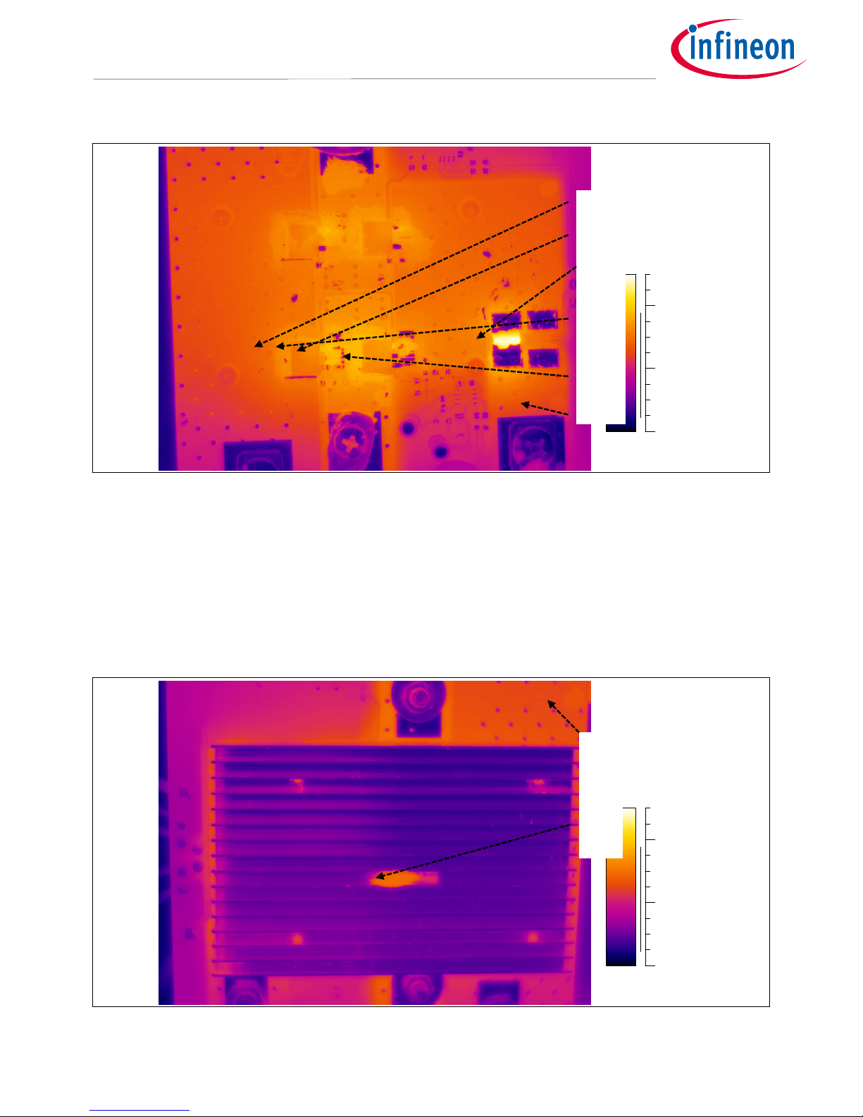
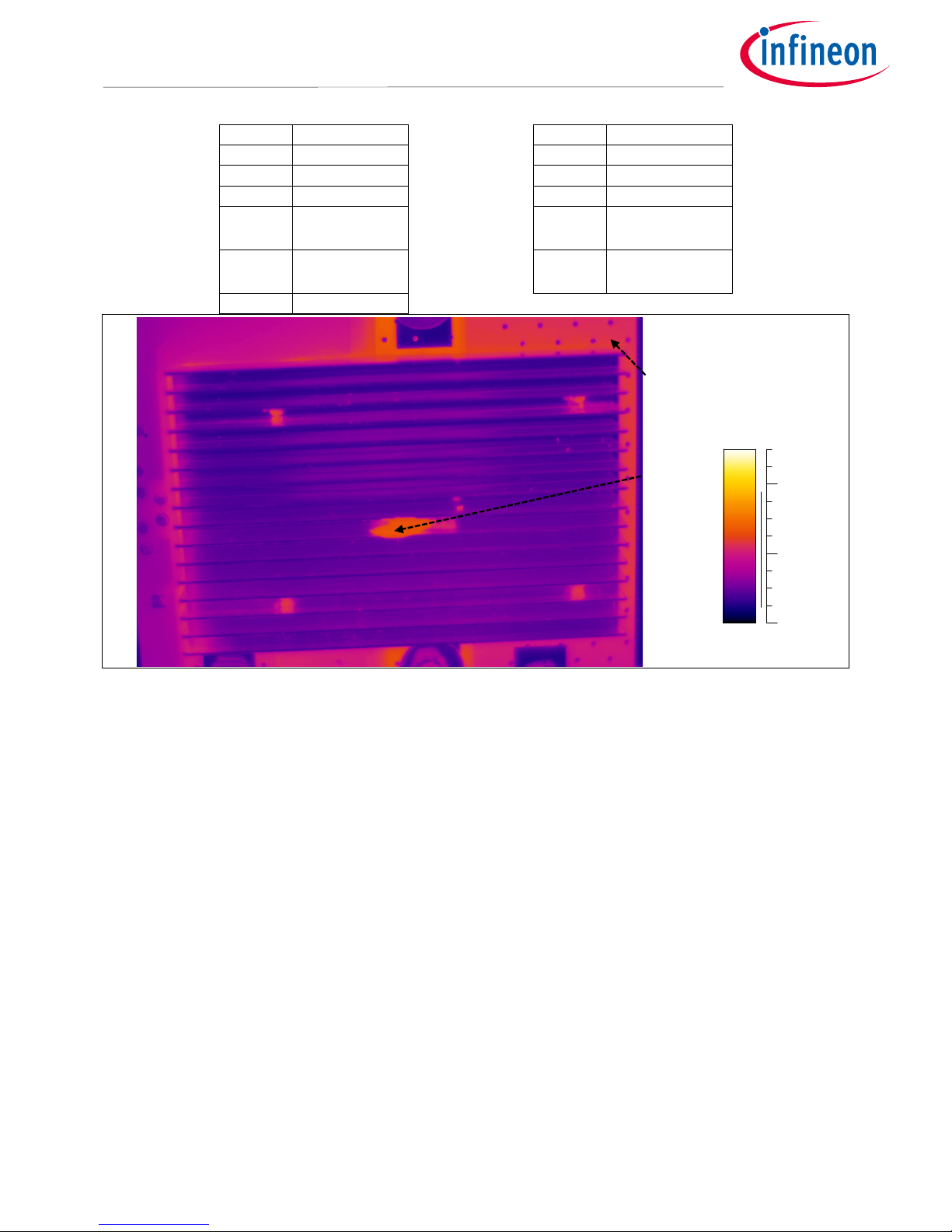
1.5.2 Performance with heatsink at the back
Figure 11 Front thermal image after 1 hour
As shown in Figure 12, the corner temperature reading (A) is 1°C higher than that with the heatsink at the front in
Figure 6. The corner temperature reading (B) as shown in Figure 13 is 2°C higher than that with the heatsink at
the front in Figure 7. It indicates that the heatsink placed at the front is slightly more effective. Its average
efficiency is 96.4 percent, shown in Table 2, which is 0.1 percent lower than that shown in Table 1 with the
heatsink at the front. The higher efficiency is consistent with lower temperature readings at locations A and B,
shown in Figures 6, 7, 12 and 13.
The PCB temperature readings shown in Figure 12 at locations C and D show 3°C difference, which indicates that
source bond wires result in additional power loss.
Figure 12 Back thermal image after 1 hour
20.0°C
70.0°C
20
40
60
20.0°C
70.0°C
20
40
60
D: 57
°
C
C:60°C
69°C
54°C
(top)
55°C
(bottom)
A: 46°C
B: 47
°
C
50°C

User Guide 11 Revision 1.0
2018-03-01
Full-bridge converter for UPS
D2PAK/ D2PAK-7 kit
UG_1801_PL16_1802_225559
Table 2 Efficiency after 1 hour
No.
Effic
ie
ncy
(percent)
1
96.6
2
96.3
3
96.4
4
96.5
5
96.4
6
96.4
7
96.3
8
96.3
Ave
rage
96.4
Stdev
0.1
1.6 Power loss estimations of MOSFETs and CS resistor
Table 3 shows the average RDS(on) at 12 VGS is 0.72 mΩ. As shown in Figure 14, the RMS current for the transformer
is 39.2 A. Therefore, the conduction power loss for each MOSFET can be estimated as 39.22×0.72/2 = 0.55 W,
which is much higher than the switching loss of 15 mW, shown in Figure 11. Based on the total power loss of 13
W, total MOSFET power loss is about 0.55 × 4/13 = 17 percent.
The power loss of the CS resistor can be estimated as 39.22× 1 = 1.5 W. This is about 12 percent of the total power
loss, which explains why it has the highest case temperature.
Table 3 RDS(on) measurements at 12 VGS
No.
R
DS(on)
(m
Ω
)
1
0.73
2
0.70
3
0.70
4
0.69
5
0.76
6
0.71
7
0.71
Ave
rage
0.72
Stdev
0.02

User Guide 12 Revision 1.0
2018-03-01
Full-bridge converter for UPS
D2PAK/ D2PAK-7 kit
UG_1801_PL16_1802_225559
Figure 13 Transformer RMS current measurement (39.2 A)
C1: I
tr
(20
A/div)

User Guide 13 Revision 1.0
2018-03-01
Full-bridge converter for UPS
D2PAK/ D2PAK-7 kit
UG_1801_PL16_1802_225559
1.7 Bill of Materials (BOM)
Item Quantity Part reference Part
description
Value Part
number
Manufacture
r
1 1 C1 Electrolytic
2700 µF 35 V
2700 µF, 35 V Nichicon
2 2 C3, C4, C5, C6 Electrolytic 5 ×
11mm
47 µF, 35 V UVK1V470
MED
Nichicon
3 4 C7, C8, C9, C10 0.1 µF × 50 V
1206 C0G
0.1 µF, 50 V CGA5L2C
OG1H104J
TDK
4 4 D1, D2, D3, D4 Diode, 100 VM,
300 MA
1N4148W 1N4148W-
7-F
Diodes Inc.
5 2 D5, D6 Diode, 100 V, 2
A
MURS 210T3 MURS
210T3
OnSemi
6 8 J2, J3, TP1,
TP2, TP3, TP4,
TP5, TP6
Test point 218
mils, 90 mils
BIAS +15 V 1502-2 Keystone
7 4 PRTN,
POWERIN,
VOUT1,
VOUT2
CONN TERM
RECT LUG 4/0-
2AWG 5/16
CX225-56HK-
QY
CXS70-14-
C
Panduit Corp
8 4 Q1, Q2, Q3,
Q4
MOSFET 40 V,
0.75 mΩ, 305 nC
IRFS7430-
7PPBF
IRFS7430 Infineon
9 4 R1, R2, R3, R4 Resistor
1206, 1/4 W, 1
percent
47 ΩRC1206FR-
0747RL
Yageo
10 4 R5, R6, R7, R8 Resistor
1206, 1/4 W, 1
percent
10 k RK73H2BT
TE1002F
KOA
11 4 R9, R10, R11,
R12
Resistor
1206, 1/4 W, 1
percent
5.1 ΩMCR10EZ
HJ5R1
Rohm
12 1 R13 Resistor
4 W
2 mΩEBWB-
N0020GET
Ohmite
User Guide 14 Revision 1.0
2018-03-01
Full-bridge converter for UPS
D2PAK/ D2PAK-7 kit
UG_1801_PL16_1802_225559
13 2 R15, R16 Resistor
1206, 1/4 W, 1
percent
1.2 ΩESR18EZP
F1R20
Rohm
14 1 R14, R17 - Not fitted Not fitted -
15 2 U1, U2 Hi/Lo gate
driver
IRS2186SPBF IRS2186SP
BF
Infineon
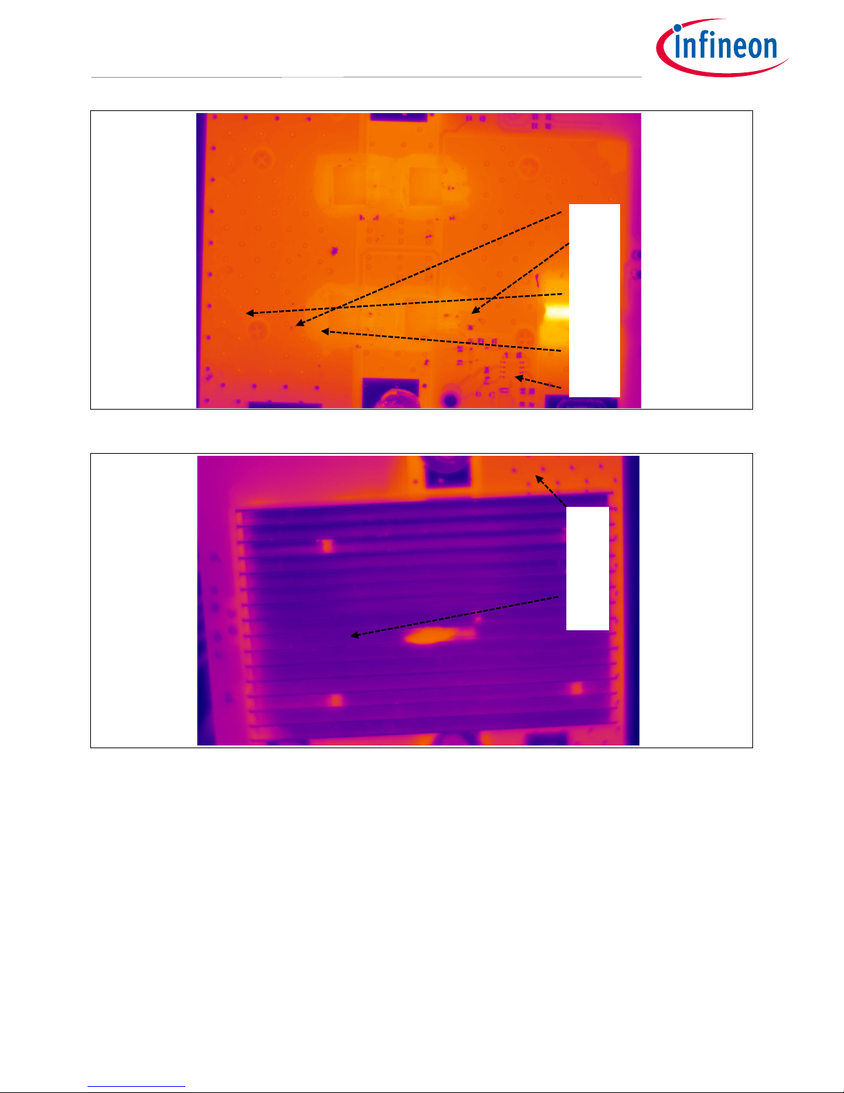
1.8 Additional results with D2PAK-7 (IRFS7430-7P)
1.8.1 Performance with heatsink at the back with 420 W load
Figure 15 shows temperature readings at the front side with a heatsink at the back. Compared with the readings
shown in Figure 12, the hottest point of the sense resistor is 5°C lower. The PCB reading at point A is 3°C lower,
both top and bottom MOSFETs are 4 to 5°C lower, and at location C the temperature reading is 7°C lower, which
shows that the source bond wires in the D27-pin package result in lower power dissipation. This is consistent with
the higher efficiencies shown in Table 4. Its average is 0.2 percent higher than the example shown in Table 2 with
the same load. Figure 16 also shows lower temperature readings with D27-pin MOSFETs. PCB location B shows
4°C lower temperature and the center 3°C lower than those shown in Figure 13. The lower power dissipation with
D27-pin parts is due to lower RDS(on), which is shown in Table 5 compared with Table 3. The average RDS(on) is 0.07
mΩlower (11 percent).
Figure 14 Front thermal image after 1 hour
Table 4 Efficiency after 1 hour Table 5 RDS(on) measurement at 12 VGS
No.
Efficiency
(percent) No. RDS(on) (mΩ)
1
96.7
1
0.64
2
96.7
2
0.66
3
96.6
3
0.64
20.0°C
70.0°C
20
40
60
C: 53
°
C
64°C
49°C
(top)
51°C
(bottom)
A: 43°C
User Guide 15 Revision 1.0
2018-03-01
Full-bridge converter for UPS
D2PAK/ D2PAK-7 kit
UG_1801_PL16_1802_225559
4
96.5
4
0.65
5
96.5
5
0.67
6
96.6
6
0.65
7
96.7
7
0.65
8 96.6 Average 0.65
Average 96.6 Stdev 0.01
Stdev
0.1
Figure 15 Back thermal image after 1 hour
1.8.2 Performance with heatsink at the back with 500 W
As shown in Figure 17, both case temperature readings at the resistor (78°C) and PCB location A (49°C) are higher
than those (64°C and 44°C) with same parts at 420 W in Figure 15 and also higher than the (69°C and 46°C) with
D2at 420 W in Figure 12. The middle of the heatsink temperature reads 55°C, as shown in Figure 18, and is 5°C
higher than that with D2parts with 420 W, as shown in Figure 13. The average efficiency with D27-pin parts
shown in Table 6 is 97.0 percent, which is 0.4 percent higher than that with 420 W, shown in Table 4.
20.0°C
70.0°C
20
40
60
B: 43
°
C
47°C
User Guide 16 Revision 1.0
2018-03-01
Full-bridge converter for UPS
D2PAK/ D2PAK-7 kit
UG_1801_PL16_1802_225559
Figure 16 Front thermal image after 1 hour with 500 W
Figure 17 Back thermal image after 1 hour with 500 W
B: 49
°
C
55°C
C: 64
°
C
78°C
(resistor)
60°C
(top)
62°C
(bottom)
A: 49°C

User Guide 17 Revision 1.0
2018-03-01
Full-bridge converter for UPS
D2PAK/ D2PAK-7 kit
UG_1801_PL16_1802_225559
Table 6 Efficiency after 1 hour
No. Efficiency
(percent)
1
97.1
2
97.0
3
97.1
4
96.9
5
97.0
6
97.1
7
97.0
8
97.1
Ave
rage
97.0
Stdev
0.1
1.8.3 Performance with heatsink at the front with 500 W
As shown in Table 7, the average efficiency is 97 percent, which is 0.4 percent higher than that with the heatsink
at the back, shown in Table 4. The temperature readings at the middle (47°C) and location A (52°C) shown in
Figure 19 are both higher than those (43°C and 45°C) shown in Figure 6 due to the additional 80 W of load.
With the same load at 500 W, the temperature reading (52°C) at A shown in Figure 19 is higher than that (49°C) in
Figure 17, while the reading (48°C) at B in Figure 20 is lower than that (49°C) in Figure 18. This behavior is
different to that with D2MOSFETs. The reason is that with the D27-pin package more heat can be transferred to
the PCB, which makes the heatsink more effective when it is located at the back. This explains why the efficiency
with the heatsink at the front is the same as that with the heatsink at the back with D27-pin MOSFETs.
Table 7 Efficiency after 1 hour
No.
Efficiency
(percent)
1
96.9
2
96.9
3
97.1
4
97.1
5
97.1
6
96.9
7
97.0
8
96.9
Ave
rage
97.0
Stdev
0.1

User Guide 18 Revision 1.0
2018-03-01
Full-bridge converter for UPS
D2PAK/ D2PAK-7 kit
UG_1801_PL16_1802_225559
Figure 18 Front thermal image after 1 hour
Figure 19 Back thermal image after 1 hour
20.0°C
80.0°C
20
40
60
80
20.0°C
80.0°C
20
40
60
80
47
°
C
A: 52°
C
B:48
°
C
69°C
65°C

User Guide 19 Revision 1.0
2018-03-01
Full-bridge converter for UPS
D2PAK/ D2PAK-7 kit
UG_1801_PL16_1802_225559
Revision history
Major changes since the last revision.
Page or reference Description of change

Trademarks of Infineon Technologies AG
AURIX™, C166™, CanPAK™, CIPOS™, CoolGaN™, CoolMOS™, CoolSET™, CoolSiC™, CORECONTROL™, CROSSAVE™, DAVE™, DI-POL™,
DrBlade™,
EasyPIM™, EconoBRIDGE™, EconoDUAL™, EconoPACK™, EconoPIM™, EiceDRIVER™, eupec™, FCOS™, HITFET™, HybridPACK™,
Infineon™,
ISOFACE™, IsoPACK™,
i-Wafer™, MIPAQ™, ModSTACK™, my-d™, NovalithIC™, OmniTune™, OPTIGA™,
OptiMOS™, ORIGA™, POWERCODE™, PRIMARION™, PrimePACK™,
PrimeSTACK™, PROFET™, PRO-SIL™, RASIC™, REAL3™, ReverSave™, SatRIC™, SIEGET™, SIPMOS™, SmartLEWIS™, SOLID FLASH™,
SPOC™,
TEMPFET™, thinQ!™, TRENCHSTOP™, TriCore™.
Trademarks updated August 2015
Other Trademarks
All referenced product or service names and trademarks are the property of their respective owners.
Edition 2018-03-01
UG_1801_PL16_1802_225559
Published by
Infineon Technologies AG
81726 Munich, Germany
© 2018 Infineon Technologies AG.
All Rights Reserved.
Do you have a question about this
document?
Email: erra[email protected]
Document reference
IMPORTANT NOTICE
The information contained in this application note is
given as a hint for the implementation of the
product only and shall in no event be regarded as a
description or warranty of a certain functionality,
condition or quality of the product. Before
implementation of the product, the recipient of this
application note must verify any function and other
technical information given herein in the real
application. Infineon Technologies hereby disclaims
any and all warranties and liabilities of any kind
(including without limitation warranties of non-
infringement of intellectual property rights of any
third party) with respect to any and all information
given in this application note.
The data contained in this document is exclusively
intended for technically trained staff. It is the
responsibility of customer’s technical departments
to evaluate the suitability of the product for the
intended application and the completeness of the
product information given in this document with
respect to such application.
For further information on the product, technology,
delivery terms and conditions and prices please
contact your nearest Infineon Technologies office
(www.infineon.com).
WARNINGS
Due to technical requirements products may contain
dangerous substances. For information on the types
in question please contact your nearest Infineon
Technologies office.
Except as otherwise explicitly approved by Infineon
Technologies in a written document signed by
authorized representatives of Infineon
Technologies, Infineon Technologies’ products may
not be used in any applications where a failure of the
product or any consequences of the use thereof can
reasonably be expected to result in personal injury.
This manual suits for next models
1
Table of contents
Other Infineon Media Converter manuals


Popular Media Converter manuals by other brands


Z3 Technology
Z3 Technology HE4K-DCK-10 Hardware specification

Speaka Professional
Speaka Professional 2615378 operating instructions

bolid
bolid S2000R user manual

ZiLOG
ZiLOG Z8 Encore! Smart Cable user manual

Jolida
Jolida Glass FX series owner's manual

Allied Telesis
Allied Telesis AT-GS2002/SP installation guide


