Infineon ILD8150 Guide

Application Note Please read the Important Notice and Warnings at the end of this document V 1.0
www.infineon.com/ref-ild8150-dc-1.5a page 1 of 28 2019-01-18
AN_1809_PL39_1810_124440
ILD8150 80 V high side buck LED driver IC with
hybrid dimming
Operation, design guide and performance
About this document
Scope and purpose
This application note introduces Infineon’s hysteretic high-side MOSFET buck DC-DC LED driver IC ILD8150 for
general lighting applications. It describes the device operation, features and component value calculations and
selection. An example of the reference design performance is shown. ILD8150 provides a highly efficient
solution up to 97 percent with superior hybrid dimming performance, and various protections such as cycle-by-
cycle current limitation and over-temperature protection.
Intended audience
This document is intended for engineers and students who design highly efficient LED drivers with a wide
dimming range.
Table of contents
About this document....................................................................................................................... 1
Table of contents............................................................................................................................ 1
1Introduction ............................................................................................................................. 3
1.1 Features ..............................................................................................................................................................3
1.2 Applications........................................................................................................................................................3
2Circuit description..................................................................................................................... 4
2.1 Operation............................................................................................................................................................4
2.1.1 Current regulation...........................................................................................................................................4
2.2 Cycle-by-cycle current limitation.......................................................................................................................5
2.2.1 OTP 5
2.2.2 UVLO 5
2.2.3 Dimming...........................................................................................................................................................6
2.2.4 Dim-to-off.........................................................................................................................................................7
2.2.5 Soft-start..........................................................................................................................................................7
2.2.6 Shut-down .......................................................................................................................................................8
2.2.7 Floating driver and bootstrap supplying........................................................................................................8
2.2.8 VIN pin ESD protection......................................................................................................................................8
2.2.9 OVP by CS pin...................................................................................................................................................9
2.2.10 Microcontroller use........................................................................................................................................9
2.3 Component selection.......................................................................................................................................10
2.3.1 Current Sense (CS) resistor ...........................................................................................................................10
2.3.2 Inductor and switching frequency selection................................................................................................10
2.3.3 Diode D selection...........................................................................................................................................10
2.3.4 Input capacitor CIN selection .........................................................................................................................11

Application Note 2 of 28 V 1.0
2019-01-23
ILD8150 80 V high side buck LED driver IC with hybrid dimming
Introduction
2.3.5 Output capacitor COUT selection....................................................................................................................11
2.3.6 Bootstrap capacitor Cboot selection...............................................................................................................11
2.4 Layout consideration .......................................................................................................................................11
2.5 Design example ................................................................................................................................................12
2.5.1 Determine RCS.................................................................................................................................................12
2.5.2 Select switching frequency ...........................................................................................................................13
2.5.1 Inductor value and its current calculation ...................................................................................................13
2.5.2 Diode selection..............................................................................................................................................13
2.5.3 CIN capacitor selection...................................................................................................................................13
2.5.4 COUT capacitor selection.................................................................................................................................13
2.5.5 Bootstrap capacitor Cboot selection...............................................................................................................14
2.5.6 VCC capacitor CVCC selection............................................................................................................................14
3Application circuit ....................................................................................................................15
3.1 Schematic layout..............................................................................................................................................15
3.2 PCB layout.........................................................................................................................................................16
4Measurement results with reference design ................................................................................17
4.1 LED current vs supply voltage..........................................................................................................................17
4.2 Dimming............................................................................................................................................................18
4.3 Soft-start...........................................................................................................................................................19
4.4 Cycle-by-cycle current limitation.....................................................................................................................19
4.5 Efficiency...........................................................................................................................................................20
4.6 Thermal behavior .............................................................................................................................................20
4.7 Output current ripple .......................................................................................................................................21
5Application with flyback converter XDPL8218 .............................................................................23
6Appendix A ..............................................................................................................................24
7References ..............................................................................................................................26
Revision history.............................................................................................................................27

Application Note 3 of 28 V 1.0
2019-01-23
ILD8150 80 V high side buck LED driver IC with hybrid dimming
Introduction
1Introduction
This application note explains the operation of Infineon’s high-side MOSFET buck LED driver IC ILD8150.
ILD8150 provides a highly efficient solution, with multiple protection features, superior hybrid PWM dimming
performance and high accuracy across all conditions –input/output voltage, dimming and temperature.
ILD8150 is a next-generation buck DC-DC LED driver recommended for general LED lighting. The target
application is a secondary stage together with AC-DC such as Power Factor Correction (PFC) flyback or PFC +
LLC. ILD8150 is flexible enough to use up to 1.5 A. The hysteretic current control is extremely fast and always
stable without the need for any loop compensation. A maximum duty cycle of up to 99 percent enables use in
applications where the input and output voltage are close to each other. It is suitable for applications with a
wide range of supply voltages from 8 V to 80 V, which gives flexibility and a clear advantage over existing 60 V
solutions.
ILD8150 operates in hybrid dimming mode, which helps to minimize LED color shift and audible noise. In the
range 12.5 to 100 percent it operates in analog dimming mode, and from 0.5 to 12.5 percent in PWM mode with
fixed output frequency fout.
ILD8150 provides high accuracy across all conditions, as well AC 100 or 120 Hz input flicker rejection across the
whole dimming range.
1.1 Features
Wide input voltage range from 8 V to 80 V
Capable of providing output current up to 1.5 A
Up to 2 MHz switching frequency
Digital soft-start
PWM dimming input up to 20 kHz
Hybrid output dimming
Typical ±3 percent output current accuracy
Very low LED current drift over-temperature
Under-Voltage Lockout (UVLO)
Cycle-by-cycle current limitation
Shut-down mode with low self-consumption
PG-DSO-8 package with and without exposed pad
Over-Temperature Protection (OTP)
1.2 Applications
LED driver for general lighting
−with single output channel
−with two output channels for tuneable white light
LED driver for horticultural lighting
−with multiple output channels

Application Note 4 of 28 V 1.0
2019-01-23
ILD8150 80 V high side buck LED driver IC with hybrid dimming
Circuit description
2Circuit description
2.1 Operation
VCC
GND
CS
VIN
SD SW
BOOT
DIM
Cfltr
Rfltr
Rcs
Iout
Vin
Cout
L
Cin
Cboot
D
Vsd
VDIM IC
Vout
CVCC
Figure 1 Typical application circuit
2.1.1 Current regulation
Figure 1 shows the typical application circuit. Current is controlled by the CS pin, which compares the voltage
drop on RCS to internal references. Output current is proportional to the voltage drop on RCS. When the CS
voltage drops below VCSL the MOSFET switches on. Current and voltage on RCS rise accordingly. When the CS
voltage achieves VCSH the MOSFET switches off, and stored energy in inductor L discharges through the diode D.
In this way, the system maintains a constant average output current as shown in Figure 2.
The output ripple of the instantaneous current is:
time [s]
IOUT [A]
1/fSW tON tOFF
ILED,AVG IOUT
Figure 2 Current regulation
Current never goes down to zero, so the system operates in Continuous Conduction Mode (CCM), where
Application Note 5 of 28 V 1.0
2019-01-23
ILD8150 80 V high side buck LED driver IC with hybrid dimming
Circuit description
and
.
Output frequency is determined by the following equation:
, where is the delay contribution, with
. This part is negligible for low frequencies but it has a strong effect at high
frequencies. Figure 3 shows the frequency curves not including the delay in blue and including the delay in red.
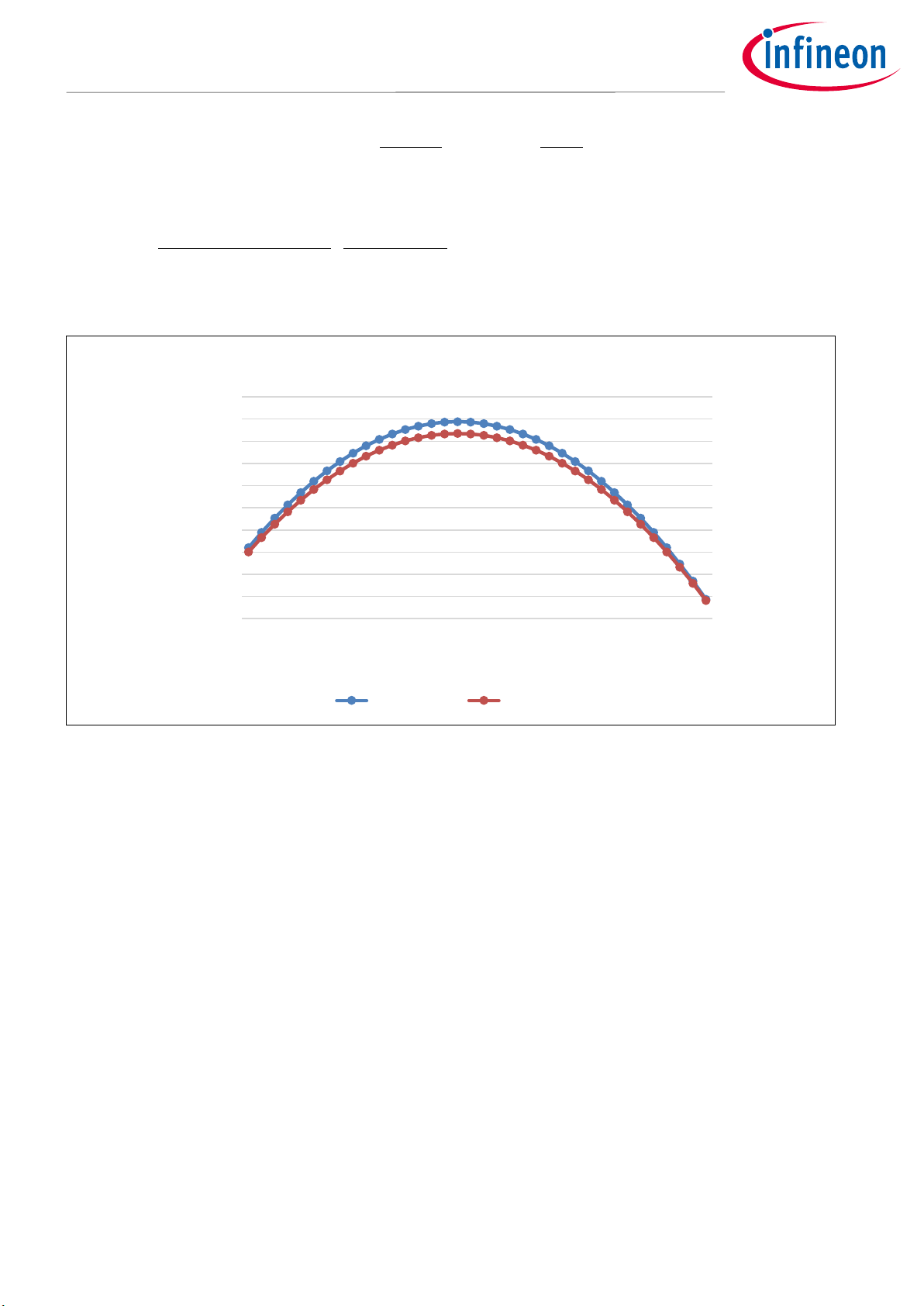
Figure 3 Typical frequency change character curve over output voltage, VIN = 80 V, L = 680 µH, RCS = 0.36 Ω, Rfltr =
1.5 kΩ, Cfltr = 180 pF
Rfltr and Cfltr are the RC filter, which reduces the noise from RCS, which can lead to unwanted operation.
2.2 Cycle-by-cycle current limitation
Because ILD8150 operates in current mode, it does not allow operation with higher current than it sets. Output
current is limited cycle-by-cycle. Thus, it safely operates even when the LED output gets shorted. RCS short-
circuit may cause damage.
2.2.1 OTP
ILD8150 has integrated OTP based on the junction temperature measurement on the chip. OTP is required to
prevent the IC from operating at a critical temperature. The high threshold when the IC turns off is TOT,OFF; the
low threshold when the IC turns on is TOT,ON.
2.2.2 UVLO
ILD8150 has hysteretic UVLO protection against operation at insufficient supply voltage. ILD8150 also has UVLO
that shuts down the IC when the minimum supply voltage drops below the internal threshold, typically
VVIN_UVLO,OFF, and releases the IC from lockout at VVIN_UVLO,ON.
0
10
20
30
40
50
60
70
80
90
100
812 16 20 24 28 32 36 40 44 48 52 56 60 64 68 72 76
Frequency, kHz
Output voltage, V
Input voltage 80 V
Without delay With delay

Application Note 6 of 28 V 1.0
2019-01-23
ILD8150 80 V high side buck LED driver IC with hybrid dimming
Circuit description
2.2.3 Dimming
Input dimming signal is PWM with minimal amplitude VDIM with frequency fDIM_input. Current accuracy over
dimming is high enough, and so is the feedback speed, that any input voltage change does not affect output
current (no flicker). The IC operates in hybrid dimming mode. The dimming curve is shown in Figure 6, which
eliminates color shift and audible noise. In the range from 12.5 to 100 percent it operates in analogue dimming
mode as shown in Figure 5, and from 0.5 to 12.5 percent in PWM mode as shown in Figure 4, with fixed output
frequency fout.
ILED,AVG
time [s]
IOUT [A]
1/fOUT
tPWM_OUT,ON
Figure 4 PWM dimming
ILED,AVG
time [s]
IOUT [A]
1/fSW tON tOFF
ILED,AVG
Figure 5 Analog dimming
100 x Iout/Iref
[%]
DPWM_IN
[%]
0.5
12.5
12.5
100
100
0.5
Analog dimming
Hybrid dimming
Figure 6 Hybrid dimming curve

Application Note 7 of 28 V 1.0
2019-01-23
ILD8150 80 V high side buck LED driver IC with hybrid dimming
Circuit description
2.2.4 Dim-to-off
ILD8150 turns the output stage off when the PWM dimming input signal duty cycle is less than
DPWM_IN,OFF, and on when the PWM dimming input signal duty cycle is higher than DPWM_IN,ON, as shown in Figure 7.
The dim-to-off hysteretic algorithm helps to avoid unstable states at the on/off boundary.
100 x Iout/Iref
[%]
DPWM_IN
[%]
0.5
0.5
DPWM_IN ,ON
DPWM_IN ,OFF
0
Figure 7 Dim-to-off
2.2.5 Soft-start
Soft-start helps to reduce component stress when the application starts. It further reduces under-shoot of the
input voltage. The soft-start is digitally preset at tSS,100 percent, defined as the maximum time to reach full light, in
the undimmed condition and up to 10*Tdim in the dimmed condition where Tdim = 1/fDIM_input. Start-up time may
also be set by a microcontroller independently of the preset soft-start. The soft-start process is shown in Figure
8. The number of current steps may vary depending on the actual and previous dimming level.
ILED,AVG,2
IOUT [A]
ILED,AVG,1
0.025
ILED,AVG,TARG
0.025
tss
Figure 8 Soft-start
Application Note 8 of 28 V 1.0
2019-01-23
ILD8150 80 V high side buck LED driver IC with hybrid dimming
Circuit description
2.2.6 Shut-down
ILD8150 has a shut-down control pin SD. If the voltage on the pin is below low-threshold VSD_IL during
recognition time more than tSD_IL the IC goes to shut-down mode with low self-consumption current. If the
voltage on the pin is higher than threshold VSD_IH during recognition time more than tSD_HI the IC resumes normal
operation through the soft-start process. Floating SD is pulled up by an internal ISD,LPU current source. To pull it
down, the current has to be more than ISD,LPU.
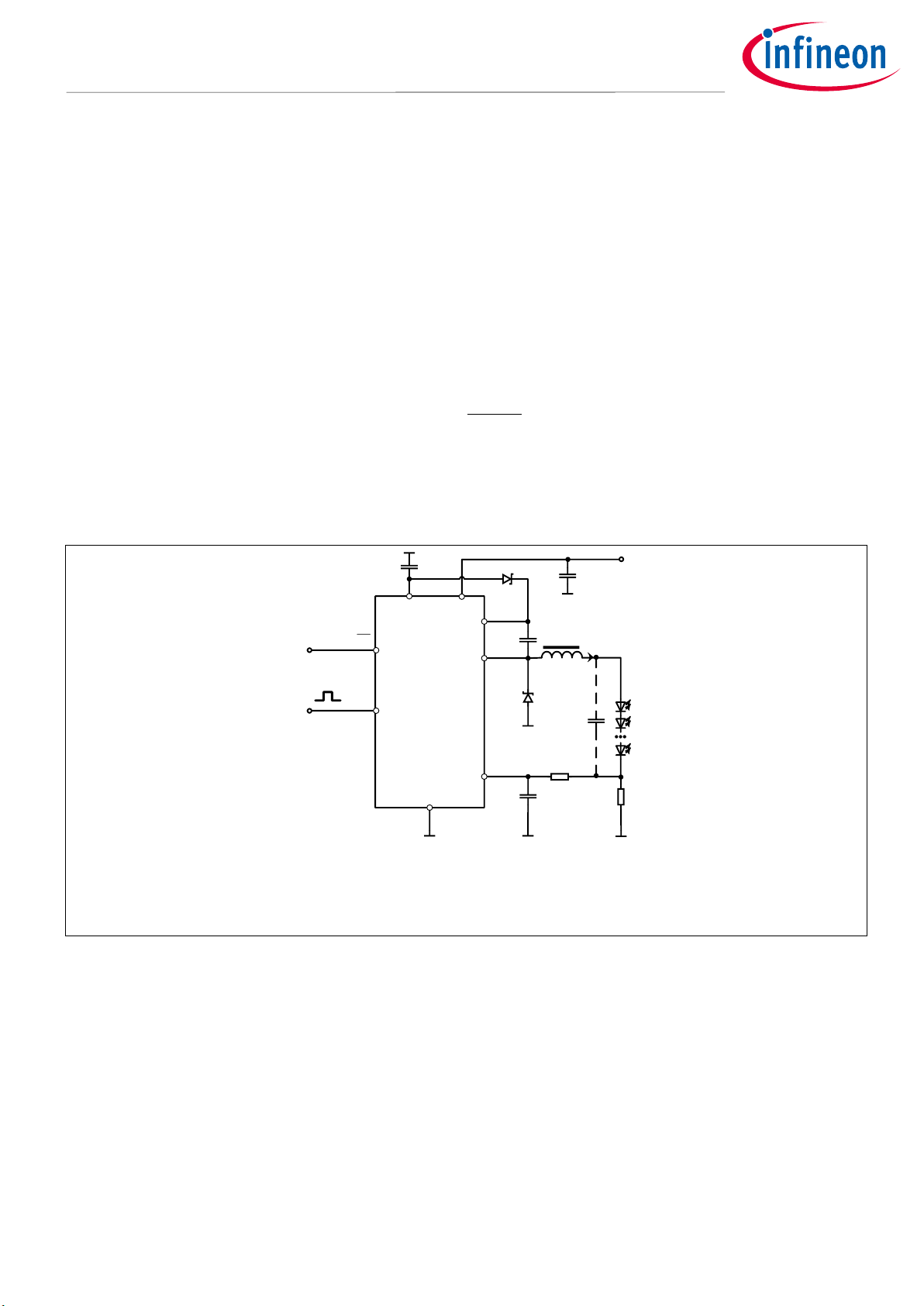
2.2.7 Floating driver and bootstrap supply
The high-side MOSFET gate driver is supplied by the bootstrap circuit. Capacitor CBOOT is charged when the high-
side MOSFET is switched off and the diode D conducts current from VCC. CBOOT can be calculated as:
Where QG is the internal MOSFET gate charge, 2.5 nC and ∆VCBOOT is voltage deviation on the bootstrap capacitor.
The internal supply circuit provides voltage to the bootstrap capacitor VCboot ≈ 8.6 V, which is a little higher than
VCC. This circuit helps to maintain the voltage in dim-to-off and standby conditions. Higher voltage improves the
RON of the internal MOSFET.
VCC
GND
CS
VIN
SD SW
BOOT
DIM
Cfltr
Rfltr
Rcs
Iout
Vin
Cout
L
Cin
Cboot
D
Vsd
VDIM IC
Dboot
CVCC
Vout
Figure 9 External bootstrap diode usage
The IC contains an internal bootstrap diode. An external high-speed signal or Shottky diode, with voltage
robustness higher than VIN, can be used between the VCC and BOOT pins as shown in Figure 9. This decreases IC
power dissipation at high switching frequency.
2.2.8 VIN pin ESD protection
The VIN pin is protected by an internal ESD structure. If VIN exceeds the absolute maximum ratings with high-
slew ratio V/ns, which may happen at HV spikes, the ESD structure conducts and absorbs the ESD stress. If the
application is a DC-DC LED driver with very low input capacitance and permanent ESD stress, it is
recommended to use an external TVS diode, which protects the IC.
Application Note 9 of 28 V 1.0
2019-01-23
ILD8150 80 V high side buck LED driver IC with hybrid dimming
Circuit description
2.2.9 OVP by CS pin
If the load is disconnected, output voltage moves to the VIN level. External output Over-Voltage Protection (OVP)
may be used as shown in Figure 10. The TVS diode conducts current when the output voltage achieves its level,
voltage on the CS pin rises to VCSH level, the high-side MOSFET switches off, and output voltage drops. TVS
diodes have a high voltage deviation connected with technology and temperature. TVS voltage should be
chosen, as this does not affect operation and also limits output voltage to the right level. RTVS and RPR limit the
current through the TVS, reduce dissipated power and reduce switching frequency in OVP mode.
VCC
GND
CS
VIN
SD SW
BOOT
DIM
Cfltr
Rfltr
Rcs
Iout
Vin
Cout
L
Cin
Cboot
DTVS
RTVS
RPR
Vsd
DIM IC
Figure 10 OVP by CS pin
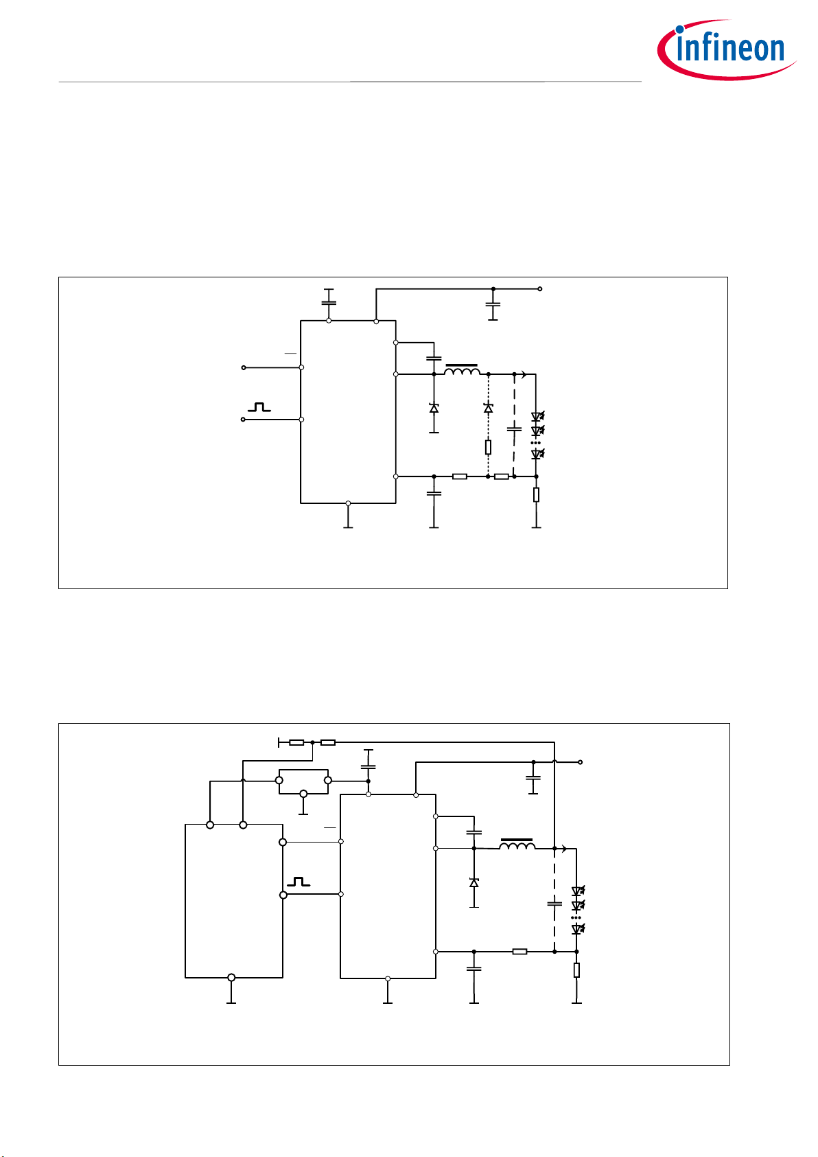
2.2.10 Microcontroller use
A microcontroller may be used together with ILD8150. This enables control of dimming, to read out the output
voltage and drive the IC into shut-down mode. The microcontroller use case is shown in Figure 11.
VCC
GND
CS
VIN
SD SW
BOOT
DIM
Cfltr
Rfltr
Rcs
Iout
Vin
Cout
L
Cin
Cboot
D
uC
Vsd
OVP
DIM
VCC
GND
ROVP2 ROVP1
LDO
IC
Figure 11 Microcontroller use

Application Note 10 of 28 V 1.0
2019-01-23
ILD8150 80 V high side buck LED driver IC with hybrid dimming
Circuit description
2.3 Component selection
2.3.1 Current Sense (CS) resistor
The average LED current is determined by the value of the CS resistor Rcs. The mean CS threshold voltage is
, VCS = 360 mV. Hence, the proper value of RCS is given by:
Power dissipated on the resistor also has to be considered:
2.3.2 Inductor and switching frequency selection
The inductor L has to maintain a constant current in the LEDs, so that the circuit operates in CCM. The inductor
value L is related to the switching frequency fSW, as shown below:
Where VIN is the input voltage, VOUT is the output voltage, VCSH and VCSL are high and low CS thresholds
accordingly, and where , tCSSW is the internal delay (less than 120 ns).
fSW should be chosen so that it never runs in an audible range less than 20 kHz across all conditions. Lower
inductance leads to smaller inductor size, but on the other hand it leads to higher switching losses, which has
to dissipate the IC and efficiency decrease. An optimal frequency in which switching losses are not so critical
should be found.
The saturation current (Isat) of the chosen inductor has to be higher than the peak LED current IPk = ILED,AVG +
∆IOUT/2.
Because output ripple is very low it is recommended to use iron powder magnetics. The core should be a closed
magnetic shape or shielded so as not to affect the IC’s sensitive inputs, such as CS.
2.3.3 Diode D selection
Once the internal MOSFET turns off, the residual inductor energy is discharged through the diode D into the
output capacitor and the LED load. Typically, a Schottky diode is used to reduce losses caused by the diode
forward voltage and reverse recovery times.
The first parameter to consider when selecting a diode is its maximum reverse voltage VBR. This voltage rating
must be higher than the maximum input voltage VIN of the circuit, VBR more than VIN.
The other two parameters defining the diode are average and RMS forward currents ID,AVG and ID,RMS:
Where D is the duty cycle of the switching waveform and is given by:

Application Note 11 of 28 V 1.0
2019-01-23
ILD8150 80 V high side buck LED driver IC with hybrid dimming
Circuit description
The diode must be chosen so that its respective current ratings are higher than these values.
2.3.4 Input capacitor CIN selection
The input current of the buck regulator is identical to the current through the MOSFET, i.e. it is pulsating and
thus causes a ripple voltage at the input. A capacitor on the VIN pin reduces this ripple voltage by providing
current when the switch is conducting. The RMS current through the input capacitor ICin,RMS is purely AC and can
be calculated from average and RMS input currents IIN,AVG and IIN,RMS as:
Hence,
Use low-ESR capacitors, especially under high switching frequency applications. With low-ESR capacitors, the
input voltage ripple can be estimated by:
The input capacitor must be chosen so that it is capable of withstanding the calculated RMS current rate and
reducing input voltage ripples to an acceptable level.
2.3.5 Output capacitor COUT selection
Due to the relatively low output ripple current, a capacitor in parallel to the LEDs is not needed in many
applications. Due to the non-linear I-V characteristics of LEDs, it is very difficult to estimate the ripple voltage
with and without an output capacitor. A generally accepted model is the approximation of LED V-I
characteristics by a voltage source VFD that models the forward voltage of the LED with a series resistor RDto
model differential resistance. Both parameters need to be determined from the LED datasheet. As a rule a VFD of
3 V and a differential resistance RDof 0.4 (this parameter is being improved with every new LED generation)
are very reasonable values for a typical white high-power LED. Consequently, for 17 LEDs in series this would
lead to a VFD of 51 V and a total RDof 6.8 . The ripple voltage without capacitor is then approximated as:
A meaningful output capacitor should therefore have an impedance at fSW, which is at least five to ten times lower
than RD:
2.3.6 Bootstrap capacitor CBOOT selection
Integrated high-side MOSFET is driven by the gate driver. The bootstrap capacitor is defined as:
Where QG is internal MOSFET gate charge 2.5 nC, is the bootstrap capacitor voltage ripple.
2.4 Layout consideration
An optimized PCB layout leads to better performance, reliability and lower cost. Certain layout guidelines must
be kept in mind while routing the PCB. The power components include the internal switch, Schottky diode,
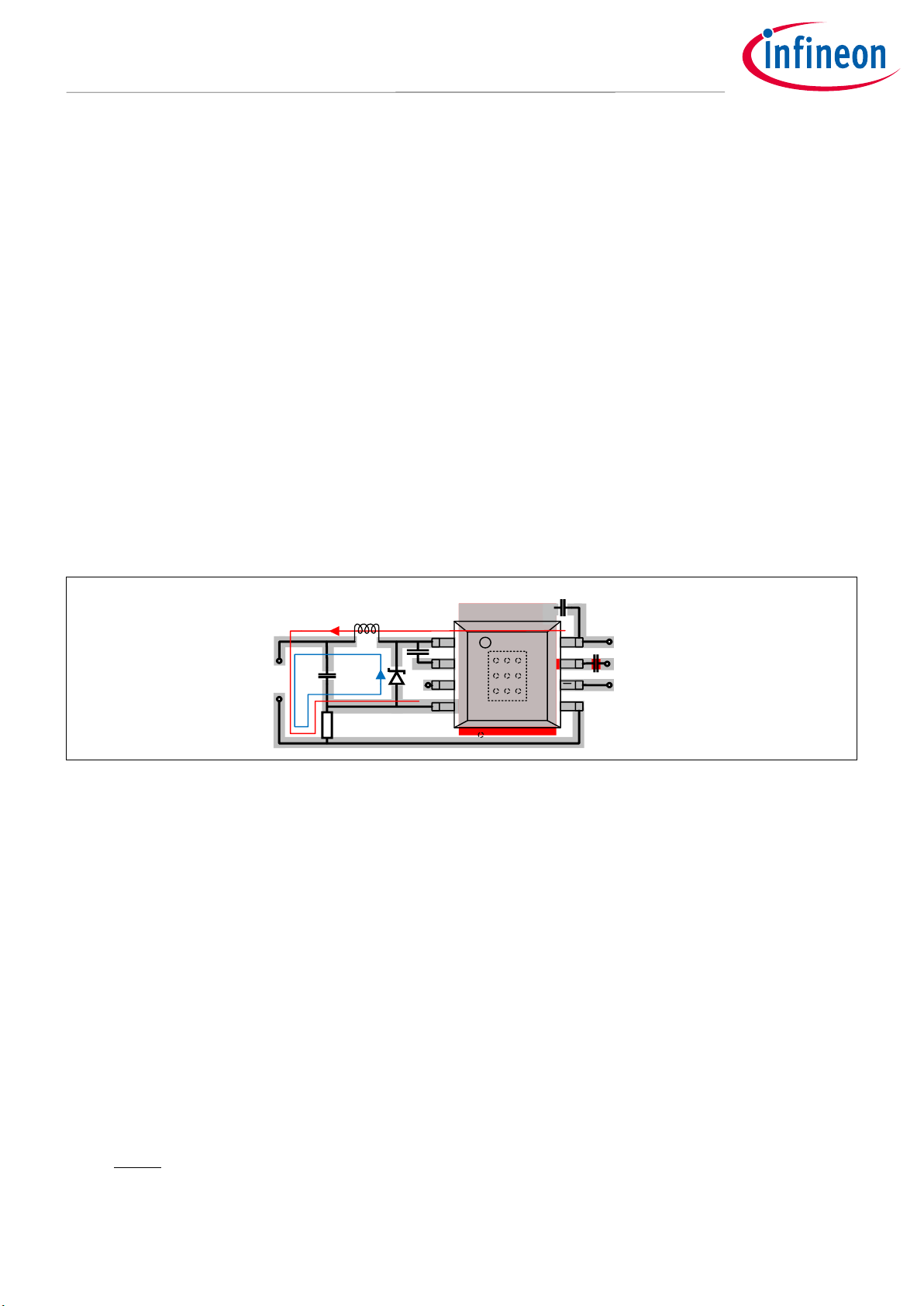
Application Note 12 of 28 V 1.0
2019-01-23
ILD8150 80 V high side buck LED driver IC with hybrid dimming
Circuit description
input capacitor, output capacitor and inductor. Place the input capacitor close to the IC, as parasitic
inductance can be minimized by minimizing trace lengths and using short and wide traces. Extra parasitic
inductance between the input capacitor’s terminals and the IC’s VIN and GND terminals creates high dV/dt due
to the switching process. This can lead to IC failure. Also, place the inductor as close as possible to the IC to
reduce radiated EMI.
The output capacitor completes the routing of all the power components. It is the final component connected
to the power ground terminal in the system. Improper output capacitor placement typically causes poor output
current regulation. To ensure optimal operation, take care to minimize the area of the power-current loop.
The small-signal control components consist of all analog and digital components indirectly related to the
power conversion, such the CS pin, which is sensitive to noise. To reduce the noise coupling from the power
stage to the control circuitry, it is necessary to keep the noisy switching traces far from the sensitive small-
signal traces. The magnetic field from the inductor may cause noise on the CS path that could in turn lead to
incorrect operation as double or triple pulses. To avoid this effect a shielded inductor should be used, but do
not place this inductor close to the sensitive CS path. To minimize noise and ensure good output current
regulation, it is critical to keep the VCS path as short as possible, and it is desirable to return the ground of the
small-signal component to a “clean” point. Poor routing of small-signal components may lead to poor output
current regulation. A power inductor placed close to the CS path can influence the regulation loop. An example
layout is shown in Figure 12.
1
2
3
4
SD
VCC
VIN
CS
5
6
7
8
DIM
BOOT
SW
GND
Thermal Via
LEDs
L
Cboot
D
Cin
Cvcc
Cout
Figure 12 Layout example
Keep separate grounds for power components, which are noisy, and for the small-signal components, which
are quiet. Then join these two grounds at one point, possibly the exposed pad under the IC, which is also the IC
ground. A grid of thermal vias should be placed under the exposed pad to improve thermal conduction. The
above guidelines ensure a well laid-out power supply design.
2.5 Design example
As an example, an LED driver with the following specification shall be designed:
VIN = 70 V
ILED,AVG = 1 A
VLED = 51 V (17 LEDs)
2.5.1 Determine RCS

Application Note 13 of 28 V 1.0
2019-01-23
ILD8150 80 V high side buck LED driver IC with hybrid dimming
Circuit description
2.5.2 Select switching frequency
80 kHz to 100 kHz may be a reasonable compromise between switching loss and inductor size. This needs to be
verified by measurement of the finished design.
2.5.1 Inductor value and its current calculation
assumedas270ns(1.5kand180pFaccordinglyFfltrkHz)
860µH
The inductor average current is 1 A, while the peak current is IPk = ILED,AVG + IOUT/2 = ILED,AVG1.083 = 1.083 A.
Saturation current ISAT of the inductor must be higher than this value.
2.5.2 Diode selection
To calculate diode currents the duty cycle D is needed:
RMS diode current:
Average diode current:
For a design with variable number of LEDs, the highest diode currents will occur at the lowest output voltage.
“1-D” is close to 1 under such conditions, and diode currents are close to the output current. In general a 1 A
diode is recommended as long as the output current is below 1 A.
The reverse blocking voltage VBR of the diode must be higher than the maximum input voltage VIN. A 100 V diode
is sufficient in this example.
2.5.3 CIN capacitor selection
, decided to choose 4.7
,
A 4.7 µF MLCC capacitor with a rated voltage of 100 V with RMS current rate of more than 0.73 A would be
recommended in this case.
2.5.4 COUT capacitor selection
The value of COUT can be estimated as:

Application Note 14 of 28 V 1.0
2019-01-23
ILD8150 80 V high side buck LED driver IC with hybrid dimming
Circuit description
For lower output voltage ripple a bigger output capacitor can be used. Because the value of this capacitor is
relatively low even for low ripple demands, a MLCC capacitor is the best choice in terms of cost, lifetime and
ESR. Switching frequency is very high and can be visible, so output capacitor may not be used just only 10 nF to
improve EMI.
2.5.5 Bootstrap capacitor CBOOT selection
= 2.5 nF (deviation voltage assumed as 1 V, was chosen as 0.2225 V MLCC).
2.5.6 VCC capacitor CVCC selection
A 100 nF 25 V MLCC capacitor was selected, which has to be placed close to pin 7.
Application Note 15 of 28 V 1.0
2019-01-23
ILD8150 80 V high side buck LED driver IC with hybrid dimming
Application circuit
3Application circuit
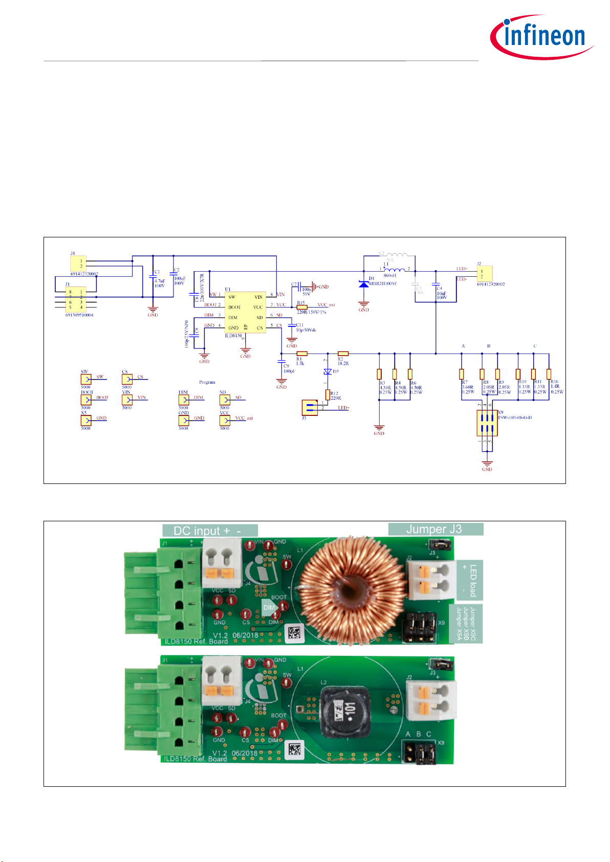
This section provides more information about the reference design available. The board is configurable to have
an output current in the range 250 mA to 1500 mA, with current adjustment by jumpers X9 A, B and C, as shown
in Figure 16. The operating voltage range for the demo board can be from 8 V to 80 V. Jumper J3 activates open-
load protection and prevents output over-voltage to 60 V. The board is designed with two optional inductors –
through-hole for high power and SMD for low power. The schematics and PCB layout are shown in Figure 13
and Figure 15 respectively. The Bill of Materials (BOM) is in Appendix A.
3.1 Schematic layout
Figure 13 Reference design circuit
Figure 14 Reference design, dimensions 82(L)x26(W)x16(H) mm
SMBJ43A
Application Note 16 of 28 V 1.0
2019-01-23
ILD8150 80 V high side buck LED driver IC with hybrid dimming
Application circuit
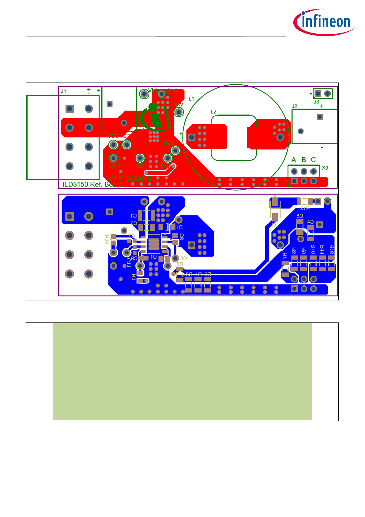
3.2 PCB layout
Figure 15 PCB layout of the reference design
Jumper X9A
Jumper X9B
Jumper X9C
Output current (mA)
-
-
-
250 (+/-3 percent)
V
-
-
350 (+/-3 percent)
-
V
-
600 (+/-3 percent)
V
V
-
700 (+/-3 percent)
-
-
V
1050 (+/-3 percent)
V
-
V
1150 (+/-3 percent)
-
V
V
1400 (+/-3 percent)
V
V
V
1500 (+/-3 percent)
Figure 16 Jumper positions vs LED current

Application Note 17 of 28 V 1.0
2019-01-23
ILD8150 80 V high side buck LED driver IC with hybrid dimming
Measurement results with reference design
4Measurement results with reference design
Table 1 Typical condition for measurement
Figure 17 shows the actual operating waveforms. The actual measured LED current is 1 A. The switching
frequency is 85 kHz and the internal DMOS transistor on the duty cycle is 74 percent.
Iout
Vsw
Figure 17 Normal operation waveform
4.1 LED current vs supply voltage
ILD8150 provides high output current accuracy despite the changes in supply voltage. Figure 18 shows the
output current vs supply voltage in the range 52 V to 70 V. Over the supply range, the output LED current only
deviates in the range of 1 percent.
VIN
RCS
Inductance
LED load
70 V
0.36 Ω
860 µH
17 pcs
Application Note 18 of 28 V 1.0
2019-01-23
ILD8150 80 V high side buck LED driver IC with hybrid dimming
Measurement results with reference design
Figure 18 Output LED current vs supply voltage
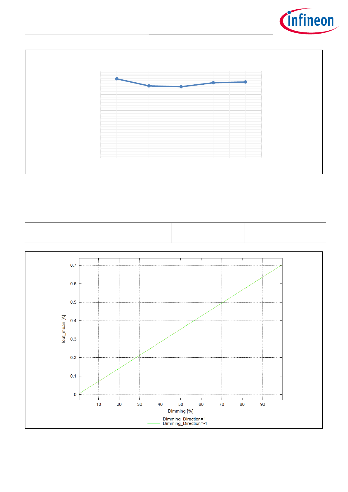
4.2 Dimming
Table 2 Condition
Figure 19 Output current vs duty cycle
1000
991 990 995 996
900
920
940
960
980
1000
52 55 60 65 70
Output current mA
Input Voltage, [V]
Output current vs Input voltage
VIN
ILED,AVG
Input PWM frequency
LED
70 V
700 mA
1 kHz
17 pcs
Application Note 19 of 28 V 1.0
2019-01-23
ILD8150 80 V high side buck LED driver IC with hybrid dimming
Measurement results with reference design
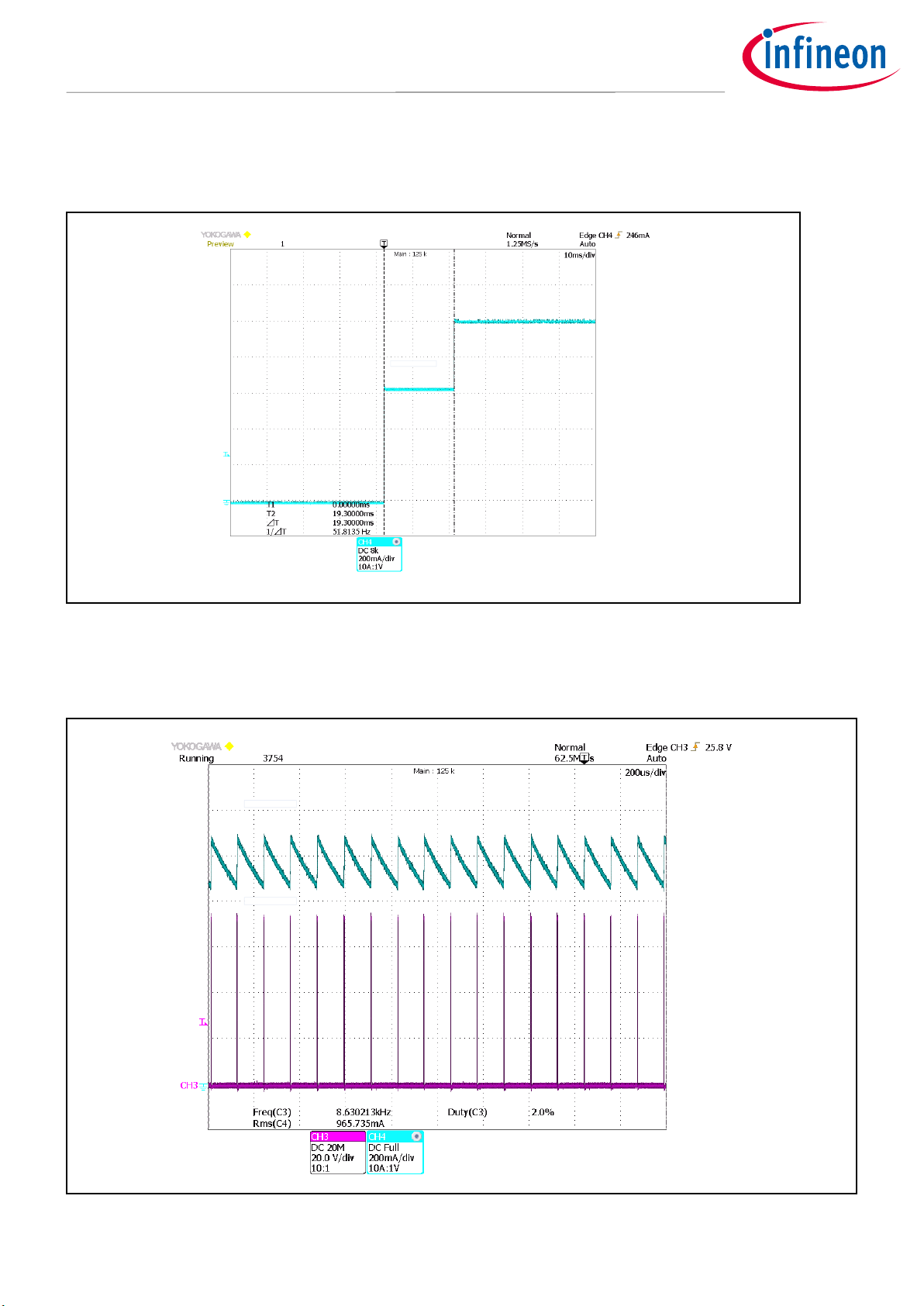
4.3 Soft-start
The soft-start process has two steps. Figure 20 shows the digital soft-start process with the steps described
earlier.
Iout
Figure 20 Soft-start, output current
4.4 Cycle-by-cycle current limitation
Figure 21 shows the waveforms under short-circuit condition where the IC limits output current cycle-by-cycle.
Iout
Vsw
Figure 21 OCP waveforms
Application Note 20 of 28 V 1.0
2019-01-23
ILD8150 80 V high side buck LED driver IC with hybrid dimming
Measurement results with reference design
4.5 Efficiency
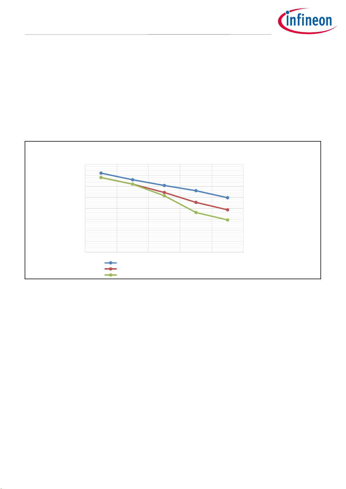
Efficiency measurement results in the input range 52 V to 70 V for 17 LEDs is shown in Figure 22. The efficiency is
measured with different inductors –860, 150 and 100 µH. It reflects the maximum switching frequency –86, 360
and 520 kHz accordingly. As seen from the character of the curves, when the difference between input and
output voltage is quite low efficiency is quite high with a wide inductance range, because the switching
frequency is relatively low. In applications with fixed output voltage, which is close to the output voltage, and
low input voltage deviation/ripple, a small inductor may be used. In applications with wide output voltage
range and input voltage ripple, such as 100 or 120 Hz, and 10 percent of ripple, which is normal on the primary
stage, switching losses create additional power dissipation. In this case inductance should be increased or
output current limited.
Figure 22 Efficiency vs supply voltage
4.6 Thermal behavior
The maximum temperature attained by the demonstration board is 73.8°C, as shown in Figure 23. The test was
performed with input 70 V and 17 LEDs.
97,6
97,3
97,0
96,8
96,5
97,4
97,1
96,7
96,3
95,9
97,4
97,1
96,6
95,8
95,5
94,0
94,5
95,0
95,5
96,0
96,5
97,0
97,5
98,0
52 55 60 65 70
Efficiency
Input Voltage
Efficiency vs Input voltage
L=860uH
L=150uH
L=100uH
Table of contents
Other Infineon Media Converter manuals


