Infineon Cypress CYW43353 User manual

www.infineon.com
Please note that Cypress is an Infineon Technologies Company.
The document following this cover page is marked as “Cypress” document as this is the
company that originally developed the product. Please note that Infineon will continue
to oer the product to new and existing customers as part of the Infineon product
portfolio.
Continuity of document content
The fact that Infineon oers the following product as part of the Infineon product
portfolio does not lead to any changes to this document. Future revisions will occur
when appropriate, and any changes will be set out on the document history page.
Continuity of ordering part numbers
Infineon continues to support existing part numbers. Please continue to use the
ordering part numbers listed in the datasheet for ordering.

PRELIMINARY
CYW43353
Single-Chip 5G MAC/Baseband/Radio with Integrated
Bluetooth 4.1 for Automotive and Industrial Applications
Cypress Semiconductor Corporation • 198 Champion Court • San Jose,CA 95134-1709 • 408-943-2600
Document Number: 002-14949 Rev. *G Revised April 13, 2020
General Description
The Cypress® CYW43353 single-chip device provides the highest level of integration for Automotive and Industrial connectivity
systems with integrated single-stream IEEE 802.11ac MAC/baseband/radio, Bluetooth 4.1. In IEEE 802.11ac mode, the WLAN
operation supports rates of MCS0–MCS9 (up to 256 QAM) in 20 MHz, 40 MHz, and 80 MHz channels for data rates up to 433.3 Mbps.
In addition, all the rates specified in IEEE 802.11a/b/g/n are supported. Included on-chip are 2.4 GHz and 5 GHz transmit amplifiers,
and receive low-noise amplifiers. Optional external PAs, LNAs, and antenna diversity are also supported.
The CYW43353 offers an SDIO v3.0 interface for high speed 802.11ac connectivity. The Bluetooth host controller is interfaced over
a 4-wire high speed UART and includes PCM for audio.
The CYW43353 brings the latest mobile connectivity technology to automotive infotainment, telematics, rear seat entertainment, and
industrial applications. Offering automotive Grade 3 (-40C to +85C) temperature performance, the CYW43353 is tested to AECQ100
environmental stress guidelines and manufactured in ISO9001 and TS16949 certified facilities.
The CYW43353 implements highly sophisticated enhanced collaborative coexistence hardware mechanisms and algorithms, which
ensure that WLAN and Bluetooth collaboration is optimized for maximum performance. In addition, coexistence support for external
radios (such as LTE cellular, GPS, and WiMAX) is provided via an external interface. As a result, enhanced overall quality for
simultaneous voice, video, and data transmission is achieved.
Cypress Part Numbering Scheme
Cypress is converting the acquired IoT part numbers from Cypress to the Cypress part numbering scheme. Due to this conversion,
there is no change in form, fit, or function as a result of offering the device with Cypress part number marking. The table provides
Cypress ordering part number that matches an existing IoT part number.
Table 1. Mapping Table for Part Number between Broadcom and Cypress
Broadcom Part Number Cypress Part Number
BCM43353 CYW43353
BCM43353LIUBG CYW43353LIUBG

Document Number: 002-14949 Rev. *G Page 2 of 113
PRELIMINARY
CYW43353
Features
IEEE 802.11x Key Features
■IEEE 802.11ac compliant.
■Single-stream spatial multiplexing up to 433.3 Mbps data
rate.
■Supports 20, 40, and 80 MHz channels with optional SGI
(256 QAM modulation).
■Full IEEE 802.11a/b/g/n legacy compatibility with enhanced
performance.
■Tx and Rx low-density parity check (LDPC) support for
improved range and power efficiency.
■Supports Rx space-time block coding (STBC)
■Supports IEEE 802.11ac/n beamforming.
■On-chip power amplifiers and low-noise amplifiers for both
bands.
■Support for optional front-end modules (FEM) with external
PAs and LNAs
■Shared Bluetooth and WLAN receive signal path eliminates
the need for an external power splitter while maintaining
excellent sensitivity for both Bluetooth and WLAN.
■Internal fractional nPLL allows support for a wide range of
reference clock frequencies
■Supports IEEE 802.15.2 external coexistence interface to
optimize bandwidth utilization with other co-located wireless
technologies such as LTE, GPS, or WiMAX
■Supports standard SDIO v3.0 (including DDR50 mode at
50 MHz and SDR104 mode at 208 MHz, 4-bit and 1-bit), and
gSPI (48 MHz) host interfaces.
■Backward compatible with SDIO v2.0 host interfaces.
■Integrated ARMCR4™ processor with tightly coupled mem-
ory for complete WLAN subsystem functionality, minimizing
the need to wake up the applications processor for standard
WLAN functions. This allows for further minimization of
power consumption, while maintaining the ability to field
upgrade with future features. On-chip memory includes 768
KB SRAM and 640 KB ROM.
■OneDriver™ software architecture for easy migration from
existing embedded WLAN and Bluetooth devices as well as
future devices.
Bluetooth Key Features
■Complies with Bluetooth Core Specification Version 4.1 for
automotive and industrial applications with provisions for sup-
porting future specifications.
■Bluetooth Class 1 or Class 2 transmitter operation.
■Supports extended synchronous connections (eSCO), for
enhanced voice quality by allowing for retransmission of
dropped packets.
■Adaptive frequency hopping (AFH) for reducing radio fre-
quency interference.
■Interface support, host controller interface (HCI) using a
high-speed UART interface and PCM for audio data.
■Supports multiple simultaneous Advanced Audio Distribution
Profiles (A2DP) for stereo sound.
■Automatic frequency detection for standard crystal and
TCXO values.
■Supports low energy host wake-up for long term system
sleep capability.

Document Number: 002-14949 Rev. *G Page 3 of 113
PRELIMINARY
CYW43353
General Features
■Supports battery voltage range from 3.0V to 4.8 supplies with
internal switching regulator.
■Programmable dynamic power management
■OTP: 502 bytes of user-accessible memory
■Nine GPIOs
■Package options:
❐145 ball WLBGA (4.87 mm × 5.413 mm, 0.4 mm pitch)
■Security:
❐WPA™ and WPA2™ (Personal) support for powerful
encryption and authentication
❐AES and TKIP in hardware for faster data encryption and
IEEE 802.11i compatibility
❐Reference WLAN subsystem provides Cisco® Compatible
Extensions (CCX, CCX 2.0, CCX 3.0, CCX 4.0, CCX 5.0)
❐Reference WLAN subsystem provides Wi-Fi Protected
Setup (WPS)
■Worldwide regulatory support: Global products supported
with worldwide homologated design.
Figure 1: Functional Block Diagram
FEM or
T/R
Switch
VIO VBAT
5 GHz WLAN TX
5 GHz WLAN RX
2.4 GHz WLAN TX
2.4 GHz WLAN/BT RX
Bluetooth TX
CYW43353
WL A N
Host I/F
Bluetooth
Host I/F
WL_REG_ON
SDIO*/SPI
BT_REG_ON
UART
BT_DEV_WAKE
BT_HOST_WAKE
CBF
I2
S
CLK_REQ
PCM
COEX
External
Coexistence I/F FEM or
T/R
Switch

Document Number: 002-14949 Rev. *G Page 4 of 113
PRELIMINARY
CYW43353
Contents
1. Overview ............................................................ 6
1.1 Overview ............................................................. 6
1.2 Features .............................................................. 8
1.3 Standards Compliance ........................................8
1.4 Automotive and Industrial Usage Model ............. 9
2. Power Supplies and Power Management ..... 10
2.1 Power Supply Topology .................................... 10
2.2 PMU Features ................................................... 10
2.3 WLAN Power Management ............................... 12
2.4 PMU Sequencing ..............................................12
2.5 Power-Off Shutdown ......................................... 13
2.6 Power-Up/Power-Down/Reset Circuits ............. 13
3. Frequency References ................................... 14
3.1 Crystal Interface and Clock Generation ............ 14
3.2 External Frequency Reference ......................... 15
3.3 Frequency Selection .........................................16
3.4 External 32.768 kHz Low-Power Oscillator ....... 17
4. Bluetooth Subsystem Overview .................... 18
4.1 Features ............................................................ 18
4.2 Bluetooth Radio ................................................. 19
4.2.1 Transmit ................................................. 19
4.2.2 Digital Modulator .................................... 19
4.2.3 Digital Demodulator and Bit Synchronizer 19
4.2.4 Power Amplifier ..................................... 19
4.2.5 Receiver ................................................ 19
4.2.6 Digital Demodulator and Bit Synchronizer 19
4.2.7 Receiver Signal Strength Indicator ........ 20
4.2.8 Local Oscillator Generation ................... 20
4.2.9 Calibration ............................................. 20
5. Bluetooth Baseband Core.............................. 21
5.1 Bluetooth 4.1 Features ......................................21
5.2 Bluetooth Low Energy ....................................... 21
5.3 Link Control Layer ............................................. 22
5.4 Test Mode Support ............................................ 22
5.5 Bluetooth Power Management Unit .................. 23
5.5.1 RF Power Management ......................... 23
5.5.2 Host Controller Power Management ..... 23
5.5.3 BBC Power Management ...................... 24
5.5.4 Wideband Speech ................................. 25
5.5.5 Packet Loss Concealment ..................... 25
5.5.6 Audio Rate-Matching Algorithms ........... 26
5.5.7 Codec Encoding .................................... 26
5.5.8 Multiple Simultaneous A2DP Audio
Streams ................................................. 26
5.6 Adaptive Frequency Hopping ............................ 26
5.7 Advanced Bluetooth/WLAN Coexistence .......... 26
5.8 Fast Connection (Interlaced Page and Inquiry
Scans) ................................................................26
6. Microprocessor and Memory Unit for
Bluetooth ......................................................... 27
6.1 RAM, ROM, and Patch Memory .........................27
6.2 Reset ..................................................................27
7. Bluetooth Peripheral Transport Unit............. 28
7.1 PCM Interface ....................................................28
7.1.1 Slot Mapping ...........................................28
7.1.2 Frame Synchronization ...........................28
7.1.3 Data Formatting ......................................28
7.1.4 Wideband Speech Support .....................28
7.1.5 Multiplexed Bluetooth Over PCM ...........28
7.1.6 PCM Interface Timing .............................30
7.2 UART Interface ..................................................34
7.3 I2S Interface .......................................................36
7.3.1 I2S Timing ...............................................36
8. WLAN Global Functions................................. 39
8.1 WLAN CPU and Memory Subsystem ................39
8.2 One-Time Programmable Memory .....................39
8.3 GPIO Interface ...................................................39
8.4 External Coexistence Interface ..........................40
8.5 UART Interface ..................................................40
8.6 JTAG Interface ...................................................40
9. WLAN Host Interfaces .................................... 41
9.1 SDIO v3.0 ...........................................................41
9.1.1 SDIO Pins ...............................................41
9.2 Generic SPI Mode ..............................................42
9.2.1 SPI Protocol ............................................43
9.2.2 gSPI Host-Device Handshake ................47
9.2.3 Boot-Up Sequence .................................47
10.Wireless LAN MAC and PHY.......................... 50
10.1 IEEE 802.11ac MAC ..........................................50
10.1.1 PSM ........................................................51
10.1.2 WEP .......................................................51
10.1.3 TXE .........................................................51
10.1.4 RXE ........................................................51
10.1.5 IFS ..........................................................52
10.1.6 TSF .........................................................52
10.1.7 NAV ........................................................52
10.2 IEEE 802.11ac PHY ...........................................52
11. WLAN Radio Subsystem ............................... 54
11.1 Receiver Path .....................................................54
11.2 Transmit Path .....................................................54
11.3 Calibration ..........................................................54

Document Number: 002-14949 Rev. *G Page 5 of 113
PRELIMINARY
CYW43353
12.Pinout and Signal Descriptions..................... 56
12.1 Ball Maps .......................................................... 56
12.2 Signal Descriptions ........................................... 57
12.3 WLAN GPIO Signals and Strapping Options .... 62
12.3.1 Multiplexed Bluetooth GPIO Signals ..... 63
12.4 GPIO/SDIO Alternative Signal Functions .......... 65
12.5 I/O States .......................................................... 66
13.DC Characteristics.......................................... 69
13.1 Absolute Maximum Ratings .............................. 69
13.2 Environmental Ratings ......................................69
13.3 Electrostatic Discharge Specifications .............. 70
13.4 Recommended Operating Conditions and DC
Characteristics .................................................. 70
14.Bluetooth RF Specifications .......................... 72
15.WLAN RF Specifications ................................ 78
15.1 Introduction ....................................................... 78
15.2 2.4 GHz Band General RF Specifications ......... 78
15.3 WLAN 2.4 GHz Receiver Performance Specifications
79
15.4 WLAN 2.4 GHz Transmitter Performance Specifica-
tions 82
15.5 WLAN 5 GHz Receiver Performance Specifications
83
15.6 WLAN 5 GHz Transmitter Performance Specifications
86
15.7 General Spurious Emissions Specifications ...... 87
16.Internal Regulator Electrical Specifications. 87
16.1 Core Buck Switching Regulator ........................ 87
16.2 3.3V LDO (LDO3P3) ......................................... 88
16.3 2.5V LDO (BTLDO2P5) ..................................... 89
16.4 CLDO ................................................................ 90
16.5 LNLDO .............................................................. 91
17.System Power Consumption ......................... 92
17.1 WLAN Current Consumption ..............................92
17.2 Bluetooth Current Consumption .........................94
18.Interface Timing and AC Characteristics ..... 95
18.1 SDIO/gSPI Timing ..............................................95
18.1.1 SDIO Default Mode Timing .....................95
18.1.2 SDIO High-Speed Mode Timing .............96
18.1.3 SDIO Bus Timing Specifications in SDR Modes
97
18.1.4 SDIO Bus Timing Specifications in DDR50
Mode 100
18.1.5 gSPI Signal Timing ...............................103
18.2 JTAG Timing ....................................................103
19.Power-Up Sequence and Timing................. 104
19.1 Sequencing of Reset and Regulator Control Signals
104
19.1.1 Description of Control Signals ..............104
19.1.2 Control Signal Timing Diagrams ...........104
20.Package Information .................................... 107
20.1 Package Thermal Characteristics ....................107
20.2 Junction Temperature Estimation and PSIJT Versus
THETAJC 107
20.3 Environmental Characteristics .........................107
21.Mechanical Information................................ 108
22.Ordering Information.................................... 110
23.IoT Resources ............................................... 110
23.1 References .......................................................110
Document History Page ............................................... 111
Added Cypress Part Numbering Scheme and Mapping Table on
Page 1. 112
Updated Cypress Logo and Copyright. 112
Updated Figure 46 (spec 002-13196 ** to *A) in Package Infor-
mation. 112
Sales, Solutions, and Legal Information .................... 113

Document Number: 002-14949 Rev. *G Page 6 of 113
PRELIMINARY
CYW43353
1. Overview
1.1 Overview
The Cypress CYW43353 single-chip device provides the highest level of integration for automotive and industrial wireless connectivity systems, with integrated IEEE 802.11
a/b/g/n/ac MAC/baseband/radio, and Bluetooth 4.1 + enhanced data rate (EDR).
It provides a small form-factor solution with minimal external components to drive down cost for mass volumes and allows for platform flexibility in size, form, and function.
The following figure shows the interconnect of all the major physical blocks in the CYW43353 and their associated external interfaces, which are described in greater detail
in the following sections.

Document Number: 002-14949 Rev. *G Page 7 of 113
PRELIMINARY
CYW43353
Figure 1. CYW43353 Block Diagram
Bluetooth WLAN
UART
I2S
PCM
Port Control
Registers
DMA
JTAG
Master
GPIO
Timers
WD
Pause
AHB2APB
AHB Bus Matrix
RAM
ROM
ARMCM3
WLAN
Master
Slave
RX/TX
BLE
LCU
APU
BlueRF
PMU
CLB FEM or
SP3T
FEM or
SPDT
Diplexer
Modem
Bluetooth RF
2.4 GHz/5 GHz 802.11ac
Dual-Band Radio
1 x 1 802.11ac PHY
DOT11MAC (D11)
Chip
Common
OTP
NIC-301 AXI Backplane
AXI2AHB
AHB2AXI
ARMCR4
TCM
RAM768KB
ROM640KB SDIOD
AXI2APB
GCI
SECI UART
and GCI-GPIOs
WLAN RAM
Sharing
WLAN BT Access
GCI Coex I/F
Shared LNA Control
and Other Coex I/Fs
VBAT
WL_REG_ON
BT_REG_ON
BT_HOST_WAKE
BT_DEV_WAKE
UART
PCM
I2S
Other GPIOs
BT
PA
32 kHz External LPO
XTAL
RF Switch Controls
SDIO 3.0
WL_HOST_WAKE
WL_DEV_WAKE
JTAG
Other GPIOs
2.4 GHz 5 GHz

Document Number: 002-14949 Rev. *G Page 8 of 113
PRELIMINARY
CYW43353
1.2 Features
The CYW43353 supports the following features:
■IEEE 802.11a/b/g/n/ac dual-band radio with virtual-simultaneous dual-band operation
■Bluetooth v4.1 + EDR with integrated Class 1 PA
■Concurrent Bluetooth and WLAN operation
■On-chip WLAN driver execution capable of supporting IEEE 802.11 functionality
■WLAN host interface options:
❐SDIO v3.0 (1-bit/4-bit)—up to 208 MHz clock rate in SDR104 mode
❐gSPI—up to 48 MHz clock rate
■BT host digital interface (which can be used concurrently with the above interfaces):
❐UART (up to 4 Mbps)
■ECI—enhanced coexistence support, ability to coordinate BT SCO transmissions around WLAN receptions
■I2S/PCM for BT audio
■HCI high-speed UART (H4, H4+, H5) transport support
■Wideband speech support (16 bits linear data, MSB first, left justified at 4K samples/s for transparent air coding, both through I2S
and PCM interface)
■Bluetooth SmartAudio® technology improves voice and music quality for automotive and industrial applications
■Bluetooth low-power inquiry and page scan
■Bluetooth Low Energy (BLE) support
■Bluetooth Packet Loss Concealment (PLC)
■Bluetooth Wide Band Speech (WBS)
■Audio rate-matching algorithms
1.3 Standards Compliance
The CYW43353 supports the following standards:
■Bluetooth 2.1 + EDR
■Bluetooth 3.0
■Bluetooth 4.1 (Bluetooth Low Energy)
■IEEE802.11ac single-stream mandatory and optional requirements for 20 MHz, 40 MHz, and 80 MHz channels
■IEEE 802.11n—Handheld Device Class (Section 11)
■IEEE 802.11a
■IEEE 802.11b
■IEEE 802.11g
■IEEE 802.11d
■IEEE 802.11h
■IEEE 802.11i

Document Number: 002-14949 Rev. *G Page 9 of 113
PRELIMINARY
CYW43353
■Security:
❐WEP
❐WPA™ Personal
❐WPA2™ Personal
❐WMM
❐WMM-PS (U-APSD)
❐WMM-SA
❐AES (Hardware Accelerator)
❐TKIP (HW Accelerator)
❐CKIP (SW Support)
■Proprietary Protocols:
❐CCXv2
❐CCXv3
❐CCXv4
❐CCXv5
■IEEE 802.15.2 Coexistence Compliance—on silicon solution compliant with IEEE 3 wire requirements
The CYW43353 will support the following future drafts/standards:
■IEEE 802.11r—Fast Roaming (between APs)
■IEEE 802.11w—Secure Management Frames
■IEEE 802.11 Extensions:
❐IEEE 802.11e QoS Enhancements (as per the WMM® specification is already supported)
❐IEEE 802.11h 5 GHz Extensions
❐IEEE 802.11i MAC Enhancements
❐IEEE 802.11k Radio Resource Measurement
1.4 Automotive and Industrial Usage Model
The CYW43353 incorporates a number of unique features to simplify integration into automotive and industrial platforms. Its flexible
PCM and UART interfaces enable it to transparently connect with existing platform circuits. In addition, the TCXO and LPO inputs
allow the use of existing automotive and industrial features to further minimize the size, power, and cost of the complete system.
■The PCM interface provides multiple modes of operation to support both master and slave as well as hybrid interfacing to single or
multiple external codec devices.
■The UART interface supports hardware flow control with tight integration to power-control sideband signaling to support the lowest
power operation.
■The crystal oscillator interface accommodates any of the typical reference frequencies used by mobile platform architectures.
■The highly linear design of the radio transceiver ensures that the device has the lowest spurious emissions output regardless of
the state of operation. It has been fully characterized in the global cellular bands.
■The transceiver design has excellent blocking and intermodulation performance in the presence of a cellular transmission (LTE,
GSM®, GPRS, CDMA, WCDMA, or iDEN).
The CYW43353 is designed to directly interface with new and existing automotive and industrial platform designs.

Document Number: 002-14949 Rev. *G Page 10 of 113
PRELIMINARY
CYW43353
2. Power Supplies and Power Management
2.1 Power Supply Topology
One buck regulator, multiple LDO regulators, and a power management unit (PMU) are integrated into the CYW43353. All regulators
are programmable via the PMU. These blocks simplify power supply design for Bluetooth and WLAN functions in embedded
designs.
A single VBAT (3.0V to 4.8 DC maximum) and VIO supply (1.8V to 3.3V) can be used, with all additional voltages being provided by
the regulators in the CYW43353.
Two control signals, BT_REG_ON and WL_REG_ON, are used to power up the regulators and take the respective section out of
reset. The CBUCK CLDO and LNLDO power up when any of the reset signals are deasserted. All regulators are powered down only
when both BT_REG_ON and WL_REG_ON are deasserted. The CLDO and LNLDO may be turned off and on based on the
dynamic demands of the digital baseband.
The CYW43353 allows for an extremely low power-consumption mode by completely shutting down the CBUCK, CLDO, and
LNLDO regulators. When in this state, LPLDO1 and LPLDO2 (which are low-power linear regulators that are supplied by the system
VIO supply) provide the CYW43353 with all the voltages it requires, further reducing leakage currents.
2.2 PMU Features
■VBAT to 1.35V (275 mA nominal, 600 mA maximum) Core-Buck (CBUCK) switching regulator
■VBAT to 3.3V (200 mA nominal, 450 mA maximum) LDO3P3
■VBAT to 2.5V (15 mA nominal, 70 mA maximum) BTLDO2P5
■1.35V to 1.2V (100 mA nominal, 150 mA maximum) LNLDO
■1.35V to 1.2V (175 mA nominal, 300 mA maximum) CLDO with bypass mode for deep-sleep
■Additional internal LDOs (not externally accessible)
The following figure shows the regulators and a typical power topology.

Document Number: 002-14949 Rev. *G Page 11 of 113
PRELIMINARY
CYW43353
Figure 2. Typical Power Topology for CYW43353
InternalLNLDO
80mA WLRF– AFE
Shaded areas are internal to the BCM 43353
WLRF– TX(2.4GHz,5GHz)
WLRF– LOGEN(2.4GHz,5GHz)
WLRF– RX/LNA(2.4GHz,5GHz)
WLRF– XTAL
WLRF– RFPLLPFD/MMD
BTRF
BTCLASS1PA
WLPA/PAD(2.4GHz,5GHz)
VDDIO_RF
WLOTP3.3V
WLRF– VCO
WLRF– CP
InternalLNLDO
80mA
InternalVCOLDO
80mA
InternalLNLDO
80mA
XTALLDO
30mA
1.2V
1.2V
1.2V
1.2V
1.2V
LNLDO
100mA
DFE/DFLL
PLL/RXTX
WLANBBPLL/DFLL
WLAN/BT/CLB/Top,alwayson
WLOTP
WLPHY
WLDIGITAL
BTDIGITAL
WL/BTSRAMs
CLDO
Peak300mA
Average175mA
(Bypassindeep
sleep)
1.2V– 1.1V
MEMLPLDO
3mA
VDDIO
BTLDO2P5
Peak70mA
Average15mA
2.5V
InternalLNLDO
25mA
InternalLNLDO
8mA
LDO3P3
Peak800–450mA
Average200mA
2.5V 2.5V
3.3V
1.2V
1.35V
WL_REG_ON
BT_REG_ON
LPLDO1
3mA
CoreBuck
Regulator
CBUCK
Peak600mA
Average275mA
1.1V
VDDIO
VBAT
0.9V

Document Number: 002-14949 Rev. *G Page 12 of 113
PRELIMINARY
CYW43353
2.3 WLAN Power Management
All areas of the chip design are optimized to minimize power consumption. Silicon processes and cell libraries were chosen to
reduce leakage current and supply voltages. Additionally, the CYW43353 integrated RAM is a high Vt memory with dynamic clock
control. The dominant supply current consumed by the RAM is leakage current only. Additionally, the CYW43353 includes an
advanced WLAN power management unit (PMU) sequencer. The PMU sequencer provides significant power savings by putting the
CYW43353 into various power management states appropriate to the current environment and activities that are being performed.
The power management unit enables and disables internal regulators, switches, and other blocks based on a computation of the
required resources and a table that describes the relationship between resources and the time needed to enable and disable them.
Power-up sequences are fully programmable. Configurable, free-running counters (running at the 32.768 kHz LPO clock frequency)
in the PMU sequencer are used to turn on and turn off individual regulators and power switches. Clock speeds are dynamically
changed (or gated altogether) for the current mode. Slower clock speeds are used wherever possible.
The CYW43353 WLAN power states are described as follows:
■Active mode— All WLAN blocks in the CYW43353 are powered up and fully functional with active carrier sensing and frame trans-
mission and receiving. All required regulators are enabled and put in the most efficient mode based on the load current. Clock
speeds are dynamically adjusted by the PMU sequencer.
■Doze mode—The radio, analog domains, and most of the linear regulators are powered down. The rest of the CYW43353
remains powered up in an IDLE state. All main clocks (PLL, crystal oscillator or TCXO) are shut down to reduce active power con-
sumption to the minimum. The 32.768 kHz LPO clock is available only for the PMU sequencer. This condition is necessary to
allow the PMU sequencer to wake up the chip and transition to Active mode. In Doze mode, the primary power consumed is due
to leakage current.
■Deep-sleep mode—Most of the chip, including both analog and digital domains, and most of the regulators are powered off. Logic
states in the digital core are saved and preserved into a retention memory in the always-ON domain before the digital core is pow-
ered off. Upon a wake-up event triggered by the PMU timers, an external interrupt, or a host resume through the SDIO bus, logic
states in the digital core are restored to their pre-deep-sleep settings to avoid lengthy HW reinitialization.
■Power-down mode—The CYW43353 is effectively powered off by shutting down all internal regulators. The chip is brought out of
this mode by external logic reenabling the internal regulators.
2.4 PMU Sequencing
The PMU sequencer is responsible for minimizing system power consumption. It enables and disables various system resources
based on a computation of the required resources and a table that describes the relationship between resources and the time
needed to enable and disable them.
Resource requests may come from several sources: clock requests from cores, the minimum resources defined in the ResourceMin
register, and the resources requested by any active resource request timers. The PMU sequencer maps clock requests into a set of
resources required to produce the requested clocks.
Each resource is in one of four states (enabled, disabled, transition_on, and transition_off) and has a timer that contains 0 when the
resource is enabled or disabled and a nonzero value in the transition states. The timer is loaded with the time_on or time_off value of
the resource when the PMU determines that the resource must be enabled or disabled. That timer decrements on each 32.768 kHz
PMU clock. When it reaches 0, the state changes from transition_off to disabled or transition_on to enabled. If the time_on value is
0, the resource can go immediately from disabled to enabled. Similarly, a time_off value of 0 indicates that the resource can go
immediately from enabled to disabled. The terms enable sequence and disable sequence refer to either the immediate transition or
the timer load-decrement sequence.

Document Number: 002-14949 Rev. *G Page 13 of 113
PRELIMINARY
CYW43353
During each clock cycle, the PMU sequencer performs the following actions:
■Computes the required resource set based on requests and the resource dependency table.
■Decrements all timers whose values are non zero. If a timer reaches 0, the PMU clears the ResourcePending bit for the resource
and inverts the ResourceState bit.
■Compares the request with the current resource status and determines which resources must be enabled or disabled.
■Initiates a disable sequence for each resource that is enabled, no longer being requested, and has no powered up dependents.
■Initiates an enable sequence for each resource that is disabled, is being requested, and has all of its dependencies enabled.
2.5 Power-Off Shutdown
The CYW43353 provides a low-power shutdown feature that allows the device to be turned off while the host, and any other devices
in the system, remain operational. When the CYW43353 is not needed in the system, VDDIO_RF and VDDC are shut down while
VDDIO remains powered. This allows the CYW43353 to be effectively off while keeping the I/O pins powered so that they do not
draw extra current from any other devices connected to the I/O.
During a low-power shut-down state, the provided VDDIO remains applied to the CYW43353, all outputs are tristated, and most
input signals are disabled. Input voltages must remain within the limits defined for normal operation. This is done to prevent current
paths or create loading on any digital signals in the system, and enables the CYW43353 to be fully integrated in an embedded
device and take full advantage of the lowest power-savings modes.
When the CYW43353 is powered on from this state, it is the same as a normal power-up, and the device does not retain any infor-
mation about its state from before it was powered down.
2.6 Power-Up/Power-Down/Reset Circuits
The CYW43353 has two signals (see Ta b l e 1 ) that enable or disable the Bluetooth and WLAN circuits and the internal regulator
blocks, allowing the host to control power consumption. For timing diagrams of these signals and the required power-up sequences,
see Section 19.: “Power-Up Sequence and Timing”.
Table 1. Power-Up/Power-Down/Reset Control Signals
Signal Description
WL_REG_ON This signal is used by the PMU (with BT_REG_ON) to power up the WLAN section. It is also OR-gated with the BT_REG_ON
input to control the internal CYW43353 regulators. When this pin is high, the regulators are enabled and the WLAN section
is out of reset. When this pin is low, the WLAN section is in reset. If BT_REG_ON and WL_REG_ON are both low, the
regulators are disabled. This pin has an internal 200 k pull-down resistor that is enabled by default. It can be disabled
through programming.
BT_REG_ON This signal is used by the PMU (with WL_REG_ON) to decide whether or not to power down the internal CYW43353
regulators. If BT_REG_ON and WL_REG_ON are low, the regulators will be disabled. This pin has an internal 200 k pull-
down resistor that is enabled by default. It can be disabled through programming.

Document Number: 002-14949 Rev. *G Page 14 of 113
PRELIMINARY
CYW43353
3. Frequency References
An external crystal is used for generating all radio frequencies and normal operation clocking. As an alternative, an external fre-
quency reference may be used. In addition, a low-power oscillator (LPO) is provided for lower power mode timing.
3.1 Crystal Interface and Clock Generation
The CYW43353 can use an external crystal to provide a frequency reference. The recommended configuration for the crystal oscil-
lator, including all external components, is shown in Figure 3. Consult the reference schematics for the latest configuration and rec-
ommended components.
Figure 3. Recommended Oscillator Configuration
A fractional-N synthesizer in the CYW43353 generates the radio frequencies, clocks, and data/packet timing, enabling the
CYW43353 to operate using a wide selection of frequency references.
For SDIO applications, the recommended default frequency reference is a 37.4 MHz crystal. The signal characteristics for the crystal
interface are listed in Table 2.
Note: Although the fractional-N synthesizer can support alternative reference frequencies, frequencies other than the default require
support to be added in the driver, plus additional extensive system testing. Contact Cypress for details.
WRF_XTAL_OUT
WRF_XTAL_IN
C*
C*
Xohms*
*Valuesdeterminedbycrystaldrive
level.Seereferenceschematicsfordetails.
37.4MHz

Document Number: 002-14949 Rev. *G Page 15 of 113
PRELIMINARY
CYW43353
3.2 External Frequency Reference
As an alternative to a crystal, an external precision frequency reference can be used. The recommended default frequency is 37.4
MHz. This must meet the phase noise requirements listed in Ta b l e 2 .
If used, the external clock should be connected to the WRF_XTAL_IN pin through an external 1000 pF coupling capacitor, as shown
in Figure 4. The internal clock buffer connected to this pin will be turned off when the CYW43353 goes into sleep mode. When the
clock buffer turns on and off, there will be a small impedance variation. Power must be supplied to the WRF_XTAL_BUCK_VDD1P5
pin.
Figure 4. Recommended Circuit to Use with an External Reference Clock
Table 2. Crystal Oscillator and External Clock—Requirements and Performance
Parameter Conditions/Notes
Crystal1External Frequency
Reference2 3
Min. Typ. Max. Min. Typ. Max. Units
Frequency 2.4 GHz and 5 GHz bands, IEEE 802.11ac
operation
35 37.4 38.4 – 37.4 – MHz
Frequency 5 GHz band, IEEE 802.11n operation only 19 37.4 38.4 35 37.438.4MHz
Frequency 2.4 GHz band IEEE 802.11n operation, and
both bands legacy 802.11a/b/g operation
only
Ranges between 19 MHz and 38.4 MHz4
Frequency tolerance
over the lifetime of the
equipment, including
temperature5
Without trimming –20 – 20 –20 – 20 ppm
Crystal load capacitance – – 12 – – – – pF
ESR – – – 60 – – – Ω
Drive level External crystal must be able to tolerate this
drive level.
200–––––µW
Input impedance
(WRF_XTAL_IN)
Resistive – – – 30k 100k – Ω
Capacitive – – 7.5 – – 7.5 pF
WRF_XTAL_IN
input low level
DC-coupled digital signal – – – 0 – 0.2 V
WRF_XTAL_IN
input high level
DC-coupled digital signal – – – 1.0 – 1.26 V
WRF_XTAL_IN
input voltage
(see Figure 4)
AC-coupled analog signal – – – 1000 – 1200 mVp-p
Duty cycle 37.4 MHz clock – – – 40 50 60 %
Phase noise6
(IEEE 802.11b/g)
37.4 MHz clock at 10 kHz offset – – – – – –129 dBc/Hz
37.4 MHz clock at 100 kHz offset – – – – – –136 dBc/Hz
Reference
Clock
NC
1000pF
WRF_XTAL_IN
WRF_XTAL_OUT

Document Number: 002-14949 Rev. *G Page 16 of 113
PRELIMINARY
CYW43353
3.3 Frequency Selection
Any frequency within the ranges specified for the crystal and TCXO reference may be used. These include not only the standard
mobile platform reference frequencies of 19.2, 19.8, 24, 26, 33.6, 37.4, and 38.4 MHz, but also other frequencies in this range with
an approximate resolution of 80 Hz. The CYW43353 must have the reference frequency set correctly in order for any of the UART or
PCM interfaces to function correctly, since all bit timing is derived from the reference frequency.
Note: he fractional-N synthesizer can support many reference frequencies. However, frequencies other than the default require
support to be added in the driver plus additional, extensive system testing. Contact Cypress for details.
The reference frequency for the CYW43353 may be set in the following ways:
■Set the xtalfreq=xxxxx parameter in the nvram.txt file (used to load the driver) to correctly match the crystal frequency.
■Autodetect any of the standard handset reference frequencies using an external LPO clock.
For applications where the reference frequency is one of the standard frequencies commonly used, the CYW43353 automatically
detects the reference frequency and programs itself to the correct reference frequency. In order for automatic frequency detection to
work correctly, the CYW43353 must have a valid and stable 32.768 kHz LPO clock that meets the requirements listed in Tab le 3 and
is present during power-on reset.
Phase noise6
(IEEE 802.11a)
37.4 MHz clock at 10 kHz offset – – – – – –137 dBc/Hz
37.4 MHz clock at 100 kHz offset – – – – – –144 dBc/Hz
Phase noise6
(IEEE 802.11n, 2.4 GHz)
37.4 MHz clock at 10 kHz offset – – – – – –134 dBc/Hz
37.4 MHz clock at 100 kHz offset – – – – – –141 dBc/Hz
Phase noise6
(IEEE 802.11n, 5 GHz)
37.4 MHz clock at 10 kHz offset – – – – – –142 dBc/Hz
37.4 MHz clock at 100 kHz offset – – – – – –149 dBc/Hz
Phase noise6
(IEEE 802.11ac, 5 GHz)
37.4 MHz clock at 10 kHz offset – – – – – –148 dBc/Hz
37.4 MHz clock at 100 kHz offset – – – – – –155 dBc/Hz
1. (Crystal) Use WRF_XTAL_IN and WRF_XTAL_OUT.
2. See External Frequency Reference for alternative connection methods.
3. For a clock reference other than 37.4 MHz, 20 × log10(f/37.4) dB should be added to the limits, where f = the reference clock frequency in MHz.
4. The frequency step size is approximately 80 Hz.
5. It is the responsibility of the equipment designer to select oscillator components that comply with these specifications.
6. Assumes that external clock has a flat phase-noise response above 100 kHz.
Table 2. Crystal Oscillator and External Clock—Requirements and Performance (Cont.)
Parameter Conditions/Notes
Crystal1External Frequency
Reference2 3
Min. Typ. Max. Min. Typ. Max. Units

Document Number: 002-14949 Rev. *G Page 17 of 113
PRELIMINARY
CYW43353
3.4 External 32.768 kHz Low-Power Oscillator
The CYW43353 uses a secondary low-frequency clock for low-power-mode timing. An external 32.768 kHz precision oscillator is
required. Use a precision external 32.768 kHz clock that meets the requirements listed in Table 3.
Table 3. External 32.768 kHz Sleep Clock Specifications
Parameter LPO Clock Units
Nominal input frequency 32.768 kHz
Frequency accuracy ±200 ppm
Duty cycle 30–70 %
Input signal amplitude 200–1800 mV, p-p
Signal type Square-wave or sine-wave –
Input impedance1
1. When power is applied or switched off.
>100k
<5
Ω
pF
Clock jitter (during initial start-up) <10,000 ppm

Document Number: 002-14949 Rev. *G Page 18 of 113
PRELIMINARY
CYW43353
4. Bluetooth Subsystem Overview
The Cypress CYW43353 is a Bluetooth 4.1 + EDR-compliant, baseband processor/2.4 GHz transceiver. It features the highest level
of integration and eliminates all critical external components, thus minimizing the footprint, power consumption, and system cost of a
Bluetooth solution.
The CYW43353 is the optimal solution for any Bluetooth voice and/or data application. The Bluetooth subsystem presents a stan-
dard Host Controller Interface (HCI) via a high-speed UART and PCM for audio. The CYW43353 incorporates all Bluetooth 4.1 fea-
tures including Secure Simple Pairing, Sniff Subrating, and Encryption Pause and Resume.
The CYW43353 Bluetooth radio transceiver provides enhanced radio performance to meet –40°C to +85°C temperature applica-
tions and the tightest integration into automotive and industrial platforms. It is fully compatible with any of the standard TCXO fre-
quencies and provides full radio compatibility to operate simultaneously with GPS, WLAN, and cellular radios.
The Bluetooth transmitter also features a Class 1 power amplifier with Class 2 capability.
4.1 Features
Major Bluetooth features of the CYW43353 include:
■Supports key features of upcoming Bluetooth standards
■Fully supports Bluetooth Core Specification version 4.1 + (Enhanced Data Rate) EDR features:
❐Adaptive Frequency Hopping (AFH)
❐Quality of Service (QoS)
❐Extended Synchronous Connections (eSCO)—Voice Connections
❐Fast Connect (interlaced page and inquiry scans)
❐Secure Simple Pairing (SSP)
❐Sniff Subrating (SSR)
❐Encryption Pause Resume (EPR)
❐Extended Inquiry Response (EIR)
❐Link Supervision Timeout (LST)
■UART baud rates up to 4 Mbps
■Supports Bluetooth 4.1 for automotive and industrial applications
■Supports maximum Bluetooth data rates over HCI UART
■Multipoint operation with up to seven active slaves
❐Maximum of seven simultaneous active ACL links
❐Maximum of three simultaneous active SCO and eSCO connections with scatternet support
■Trigger Cypress fast connect (TBFC)
■Narrowband and wideband packet loss concealment
■Scatternet operation with up to four active piconets with background scan and support for scatter mode
■High-speed HCI UART transport support with low-power out-of-band BT_DEV_WAKE and BT_HOST_WAKE signaling (see Host
Controller Power Management )
■Channel quality driven data rate and packet type selection
■Standard Bluetooth test modes
■Extended radio and production test mode features
■Full support for power savings modes

Document Number: 002-14949 Rev. *G Page 19 of 113
PRELIMINARY
CYW43353
❐Bluetooth clock request
❐Bluetooth standard sniff
❐Deep-sleep modes and software regulator shutdown
■TCXO input and autodetection of all standard handset clock frequencies. Also supports a low-power crystal, which can be used
during power save mode for better timing accuracy.
4.2 Bluetooth Radio
The CYW43353 has an integrated radio transceiver that has been optimized for use in 2.4 GHz Bluetooth wireless systems. It has
been designed to provide low-power, low-cost, robust communications for applications operating in the globally available 2.4 GHz
unlicensed ISM band. It is fully compliant with the Bluetooth Radio Specification and EDR specification and meets or exceeds the
requirements to provide the highest communication link quality.
4.2.1 Transmit
The CYW43353 features a fully integrated zero-IF transmitter. The baseband transmit data is GFSK-modulated in the modem block
and upconverted to the 2.4 GHz ISM band in the transmitter path. The transmitter path performs signal filtering, I/Q upconversion,
output power amplification, and RF filtering. The transmitter path also incorporates /4-DQPSK and 8-DPSK modulations for 2 Mbps
and 3 Mbps EDR support, respectively. The transmitter section is compatible to the Bluetooth Low Energy specification. The trans-
mitter PA bias can also be adjusted to provide Bluetooth Class 1 or Class 2 operation.
4.2.2 Digital Modulator
The digital modulator performs the data modulation and filtering required for the GFSK, /4-DQPSK, and
8-DPSK signal. The fully digital modulator minimizes any frequency drift or anomalies in the modulation characteristics of the trans-
mitted signal and is much more stable than direct VCO modulation schemes.
4.2.3 Digital Demodulator and Bit Synchronizer
The digital demodulator and bit synchronizer take the low-IF received signal and perform an optimal frequency tracking and bit-syn-
chronization algorithm.
4.2.4 Power Amplifier
The fully integrated PA supports Class 1 or Class 2 output using a highly linearized, temperature-compensated design. This provides
greater flexibility in front-end matching and filtering. Due to the linear nature of the PA combined with some integrated filtering, exter-
nal filtering is required to meet the Bluetooth and regulatory harmonic and spurious requirements. For integrated telematics applica-
tions in which Bluetooth is integrated next to the cellular radio, external filtering can be applied to achieve near-thermal-noise levels
for spurious and radiated noise emissions. The transmitter features a sophisticated on-chip transmit signal strength indicator (TSSI)
block to keep the absolute output power variation within a tight range across process, voltage, and temperature.
4.2.5 Receiver
The receiver path uses a low-IF scheme to downconvert the received signal for demodulation in the digital demodulator and bit syn-
chronizer. The receiver path provides a high degree of linearity, an extended dynamic range, and high-order on-chip channel filtering
to ensure reliable operation in the noisy 2.4 GHz ISM band. The front-end topology, with built-in out-of-band attenuation, enables the
CYW43353 to be used in most applications with minimal off-chip filtering. For integrated telematics operation, in which the Bluetooth
function is integrated close to the cellular transmitter, external filtering is required to eliminate the desensitization of the receiver by
the cellular transmit signal.
4.2.6 Digital Demodulator and Bit Synchronizer
The digital demodulator and bit synchronizer take the low-IF received signal and perform an optimal frequency tracking and bit syn-
chronization algorithm.
This manual suits for next models
3
Table of contents
Other Infineon Single Board Computer manuals
Popular Single Board Computer manuals by other brands

Sferalabs
Sferalabs IPBB20R user guide
IEI Technology
IEI Technology PCIE-Q370 Quick installation guide
IEI Technology
IEI Technology WAFER-PV-D4252 user manual
Connect Tech
Connect Tech PCIe/104 user manual
Kontron
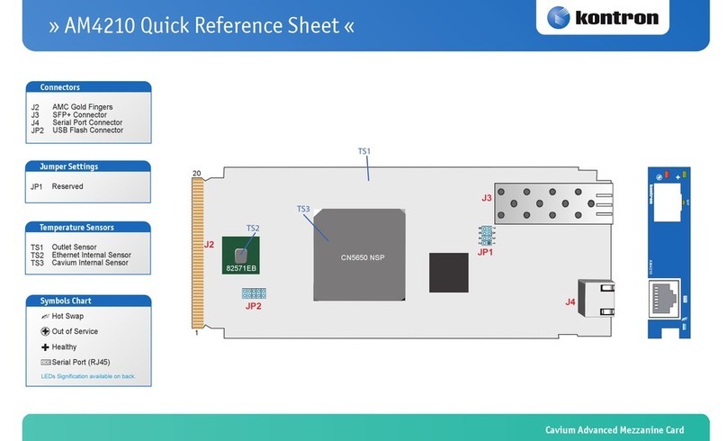
Kontron AM4210 Quick reference sheet

Premier Farnell
Premier Farnell Embest SBC-PH8700 user manual
